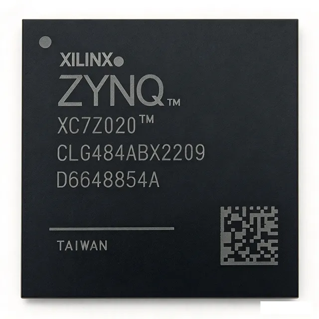
XC7Z020-1CLG484I - Zynq-7000 SoC 667MHz Dual ARM Cortex-A9 | AMD/Xilinx
MPN: XC7Z020-1CLG484I ✓ Active| Qty | Unit Price | Extended |
|---|---|---|
| 1 | $78.75 | $78.75 |
| 10 | $56.875 | $568.75 |
| 100 | $50.3125 | $5,031.25 |
| 500 | $48.125 | $24,062.50 |
| 1,000 | $45.9375 | $45,937.50 |
XC7Z020-1CLG484I Overview
A SoC FPGA such as the Zynq-7000 is a single silicon device that fuses a hard processor subsystem (HSS) and a soft FPGA fabric. The processor subsystem runs software (Linux, RTOS, bare-metal), while the programmable logic provides hardware acceleration, custom I/O, and parallel data-path extensions. Zynq-7000 devices sit within the broader taxonomy of heterogeneous compute devices, alongside MPSoC and Versal Adaptive SoC families from AMD/Xilinx. This hybrid architecture is ideal for embedded systems that require both deterministic real-time control and high-throughput data processing.
Key features include dual ARM Cortex-A9 cores with NEON SIMD and single/double precision FPU, on-chip L1 caches (32 KB I-cache, 32 KB D-cache per core) and 512 KB L2 cache, integrated Memory Controller for DDR3/DDR3L/LPDDR2, dual USB 2.0 OTG, dual Gigabit Ethernet MACs, dual SD/SDIO controllers, and 2x UART, 2x SPI, 2x I2C peripheral interfaces. The integrated Artix-7 FPGA fabric includes 85K logic cells, 4.9 Mb block RAM, and 220 DSP slices.
The Zynq-7000 architecture uses a tightly coupled AXI interconnect between the PS and PL, allowing hardware-accelerated peripherals to communicate with the processor at high bandwidth with predictable latency. The CLG484 package exposes multiple high-performance (HP) and high-range (HR) I/O banks for DDR interfacing and general-purpose I/O.
Typical applications include industrial motor drives, machine vision, software-defined radio, ADAS driver assistance systems, medical imaging, and embedded vision. The wide temperature range and -1 speed grade make the XC7Z020-1CLG484I well suited for industrial control and factory automation.
When designing with this device, careful attention must be paid to PCB layout, power-rail sequencing, and DDR signal integrity. Use Vivado Design Suite and Vitis for hardware/software co-design, and refer to the official Zynq-7000 datasheet (DS187) and PCB design guide (UG933).
This page synthesizes distributor pricing, drop-in alternatives, and practical design notes not found in the manufacturer datasheet.
Drop-in alternatives for XC7Z020-1CLG484I — same package, pin-to-pin compatible. Different-package parts requiring PCB rework are excluded.
Variants in this series
Same-series models that are drop-in compatible with XC7Z020-1CLG484I (same form factor and footprint) — differing in Logic Cells, Mounting Type, Package, Speed Grade.
Quick Comparison Tool — Select alternative parts for side-by-side comparison:
XC7Z020-2CLG484I
✓ In Stock
$49 / Unit
View Datasheet →XC7Z020-1CLG484C
📋 Reference alternative (not in catalog)
XC7Z020-1CLG400I
📋 Reference alternative (not in catalog)
XC7Z020-1CLG484I Maximum Ratings & Electrical Characteristics
| Family | Zynq-7000 All Programmable SoC |
| Device | XC7Z020 |
| Speed Grade | -1 |
| Processing System | Dual ARM Cortex-A9 MPCore |
| Max Processor Clock | 667 MHz |
| FPGA Fabric | Artix-7 |
| Logic Cells | 85K |
| Block RAM | 4.9 Mb |
| DSP Slices | 220 |
| Package | 484-ball CSBGA (CLG484) 19x19 mm |
| Temperature Grade | Industrial (-40C to +100C) |
| L1 Cache (per core) | 32 KB I-cache + 32 KB D-cache |
| L2 Cache | 512 KB |
| Mounting Type | Surface Mount (BGA) |
| RoHS Status | Compliant |
XC7Z020-1CLG484I 484-ball csbga (clg484) 19x19 mm Pin Configuration Guide
Pin configuration for XC7Z020-1CLG484I (484-ball csbga (clg484) 19x19 mm package). This digital IC includes GPIO, communication interfaces (UART, SPI, I2C), and power pins. Refer to the manufacturer datasheet for alternate pin functions and configuration options. Essential for embedded system design and PCB layout.

No detailed pinout data available for XC7Z020-1CLG484I.
Refer to the datasheet for full pin configuration.
Typical Applications
XC7Z020-1CLG484I is suitable for 6 applications: Industrial Motor Control, Machine Vision Systems, Software-Defined Radio, Embedded IoT Gateways, Medical Imaging and Diagnostic Equipment, ADAS and Driver Assistance.
Industrial Motor Control
The XC7Z020-1CLG484I fits industrial motor control applications by combining a real-time capable ARM Cortex-A9 processor with hardware-accelerated FPGA fabric. The 667 MHz dual-core CPU handles motion-control algorithms and EtherCAT/EtherNet/IP stack processing, while the Artix-7 PL fabric implements custom PWM generators, encoder interfaces, and current-sampling logic with sub-microsecond latency. The 220 DSP slices accelerate Field-Oriented Control (FOC) and PID computations. The CLG484 package exposes sufficient HP/HR I/O banks for multi-axis servo drive designs.
Recommended
Machine Vision Systems
The XC7Z020-1CLG484I fits machine vision systems where image acquisition, preprocessing, and inference must run on a single chip. The dual ARM Cortex-A9 cores run Linux with OpenCV or vendor SDKs, while the Artix-7 fabric implements hardware-accelerated image preprocessing (filtering, morphology, Bayer-to-RGB conversion) at line rates exceeding 200 MP/s. The integrated DDR3 controller supports high-bandwidth camera sensor data, and the 4.9 Mb block RAM serves as fast frame-buffer memory. Gigabit Ethernet enables GigE Vision network connectivity.
Recommended
Software-Defined Radio
The XC7Z020-1CLG484I fits software-defined radio platforms by providing both baseband signal processing in the FPGA fabric and protocol stack execution on the ARM cores. The 220 DSP slices implement digital down-conversion, channelization, and modulation/demodulation at sample rates exceeding 100 MSPS. The 667 MHz ARM Cortex-A9 handles network protocols, MAC layer, and user interface. The CLG484 package exposes GTX transceivers (where equipped) and sufficient I/O for ADC/DAC interfacing.
Recommended
Embedded IoT Gateways
The XC7Z020-1CLG484I fits embedded IoT gateways requiring protocol translation between industrial fieldbuses (Modbus, CAN, RS-485) and IP networks (Ethernet, Wi-Fi, cellular). The dual ARM Cortex-A9 cores run Linux with containerized services such as Node-RED, MQTT brokers, and OPC UA servers. The FPGA fabric implements custom industrial protocol interfaces, hardware-accelerated encryption, and real-time sensor preprocessing. The integrated dual Gigabit Ethernet MACs enable network router/switch functionality.
Recommended
Medical Imaging and Diagnostic Equipment
The XC7Z020-1CLG484I fits medical imaging and diagnostic equipment by providing certified hardware platforms with deterministic processing. The FPGA fabric implements high-speed data acquisition from ultrasound transducers or X-ray detectors, while the ARM Cortex-A9 cores run display drivers and user-interface software. The industrial temperature grade (-40C to +100C) supports a wide range of clinical environments. Hardware accelerators in the PL deliver real-time image enhancement, beam steering, and Doppler processing.
Recommended
ADAS and Driver Assistance
The XC7Z020-1CLG484I fits ADAS applications including surround-view, lane-departure warning, and front-camera perception. The FPGA fabric implements real-time image stitching, perspective transform, and object-detection preprocessing at 30-60 fps. The ARM Cortex-A9 cores run perception algorithms, sensor fusion, and vehicle network communication (CAN, Automotive Ethernet). The industrial temperature grade supports under-hood and cabin automotive environments. Camera link interfaces are implemented in the PL fabric using HP I/O banks.
Recommended
Recommended Products Summary
Engineering reference data for XC7Z020-1CLG484I — comparison, design guidance, and compliance information.
Selection Guide
Comparison with Alternatives
| Parameter | This Product | XC7Z020-2CLG484I | XC7Z020-1CLG484C | XC7Z020-1CLG400I |
|---|---|---|---|---|
| Package | 484-ball CSBGA (CLG484) | 484-ball CSBGA (CLG484) - same | 484-ball CSBGA (CLG484) - same | 400-ball CSBGA (CLG400) - smaller |
| Brand | AMD (Xilinx) | AMD (Xilinx) | AMD (Xilinx) | AMD (Xilinx) |
| Speed Grade | -1 | -2 (faster Fmax) | -1 (same) | -1 (same) |
| Temperature Grade | Industrial (-40C to +100C) | Industrial | Commercial (0C to +85C) | Industrial |
| Logic Cells | 85K | 85K | 85K | 85K |
| Processor Clock | 667 MHz | 667 MHz | 667 MHz | 667 MHz |
| DSP Slices | 220 | 220 | 220 | 220 |
| Block RAM | 4.9 Mb | 4.9 Mb | 4.9 Mb | 4.9 Mb |
Key Differentiators
- Identical silicon with higher FPGA fabric Fmax (vs XC7Z020-2CLG484I)
- Lower cost commercial temperature variant (vs XC7Z020-1CLG484C)
- Smaller footprint option with reduced I/O (vs XC7Z020-1CLG400I)
Design Notes
The Zynq-7000 XC7Z020 requires multiple power rails: VCCPINT (1.0V core), VCCPAUX (1.8V auxiliary), VCCPLL (1.8V PLL), VCCO_MIO (1.8V-3.3V MIO banks), VCCO_DDR (1.5V DDR3), and VCCO_HP/HR (1.2V-3.3V PL I/O). Power sequencing requirements per AMD DS187 mandate VCCPINT must rise before or simultaneously with VCCPAUX and VCCO rails. Use a dedicated PMIC such as the TPS652170RSLT or discrete LDO/DCDC combination with proper power-good sequencing. Estimated: at 667 MHz CPU and 100 MHz fabric, total power consumption is approximately 2-4W depending on utilization.
The CLG484 BGA package has a thermal resistance (theta_JA) of approximately 15-20 C/W depending on PCB stack-up. Estimated: at 3W total power dissipation with 4-layer FR4 PCB and minimal copper, junction-to-ambient delta is 60C. A thermal via array beneath the BGA and at least 8-layer PCB stack-up with internal copper pours is strongly recommended for industrial temperature applications operating above 1.5W. Consider heatsink attachment for closed-enclosure designs.
The CLG484 19x19 mm BGA requires 0.8 mm ball pitch with 0.4 mm pad diameter. PCB design rules per UG933 mandate microvia-in-pad technology for breakout routing on top layers. Use a 1-2-1 or 1-2-1-2-1 HDI stack-up with laser-drilled microvias. DDR3 signal traces require 50 ohm single-ended controlled impedance with length matching within 25 mils. Maintain at least 4 ground return vias around high-speed signal transitions. All BGA pads must use NSMD (Non-Solder Mask Defined) geometry per industry standard.
Common pitfalls when designing with the XC7Z020 include: (1) incorrect boot mode configuration - the MODE pins [3:0] must be properly pulled to select JTAG, QSPI, SD, or NAND boot source; (2) omitting decoupling capacitors - at least 100 nF and 4.7 uF decoupling per power pin per AMD recommendation; (3) violating MIO bank voltage constraints when mixing 1.8V and 3.3V peripherals; (4) not using Vivado Board File or XDC constraints for pin assignments; (5) selecting incorrect DDR termination - DDR3 requires VTT termination at 0.75V with proper ODT calibration.
Compliance Information
RoHS and REACH compliant per AMD/Xilinx product page. Not AEC-Q100 qualified; for automotive applications consider XC7Z020-1CLG484Q or similar Q-grade parts.







