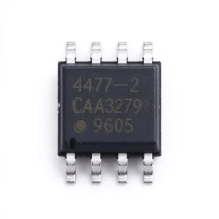
AD548KR - Low-Power Precision BiFET Op Amp | Analog Devices
料号: AD548KR ✗ 停产AD548KR 概述
A BiFET operational amplifier is an input stage that uses field-effect transistors to achieve very high input impedance and low input bias current. Within the amplifier hierarchy, the AD548KR is a voltage-feedback operational amplifier, also classified as a precision low-noise amplifier and a low-power analog signal-conditioning IC. Its combination of low supply current and precision DC performance supports battery-powered instruments, industrial measurement systems, and low-level sensor interfaces.
The AD548 family is specified for low quiescent current of 170 uA typical and 200 uA maximum. Its warmed input bias current reaches 10 pA maximum, while offset voltage is limited to 250 uV maximum and offset drift to 2 uV/°C maximum. These characteristics make the amplifier suitable for high-impedance transducers, current measurements, and precision feedback networks where bias current and thermal drift can materially affect accuracy.
AC performance includes a 1 MHz unity-gain bandwidth and a 1 V/us slew rate. The Analog Devices AD548 data sheet identifies the AD548 as pin compatible with the LF441, TL061, and AD542, allowing designers to improve performance while reducing power dissipation by as much as 85%. A single-amplifier, single-supply-compatible topology provides flexibility for battery-operated and dual-supply analog systems.
Typical uses include low-level sensor amplification, biomedical instrumentation, industrial process measurement, photodiode signal chains, precision current sensing, and portable data-acquisition equipment. The low bias current benefits high-source-impedance sensors, while the low quiescent current limits supply consumption in battery-powered systems.
The primary PCB-design consideration is input bias-current management. Keep sensitive input traces short, use guarded or low-leakage construction where appropriate, and place the amplifier input network close to the device. Confirm the SOIC-8 footprint, supply decoupling, output-load limits, and stability requirements against the manufacturer data sheet before production release.
This page combines manufacturer specifications, lifecycle information, pin-compatible comparison data, application guidance, and design-focused selection criteria to support faster engineering evaluation. It also identifies where replacement decisions require checking exact grade, package, supply range, and electrical limits.
直接替换替代料: AD548KR ——相同封装,引脚兼容。需要 PCB 改动的不同封装料号已排除。
AD548JRZ
✅ 直接替换📋 参考替代料(不在目录中)
AD548JRZ-REEL
✅ 直接替换📋 参考替代料(不在目录中)
AD548JR
✅ 直接替换 ⚠️ 规格未核验📋 参考替代料(不在目录中)
AD548JZ
✅ 直接替换 ⚠️ 规格未核验📋 参考替代料(不在目录中)
AD548KR 最大额定值与电气特性
| Amplifier Type | Precision, low-power BiFET operational amplifier |
| Number of Amplifiers | 1 amplifier |
| Maximum Supply Voltage | 18 V |
| Operating Supply Range | ±4.5 V to ±18 V |
| 静态电流 | 170 uA typical, 200 uA maximum |
| Input Bias Current | 10 pA maximum, warmed |
| Offset Voltage | 250 uV maximum |
| Offset Voltage Drift | 2 uV/°C maximum |
| Unity-Gain Bandwidth | 1 MHz |
| Slew Rate | 1 V/us |
| Input Noise Voltage | 2 V p-p |
| 封装 | 8-lead SOIC |
| 安装类型 | Surface mount |
| Maximum Power Dissipation | 500 mW |
| AD548B Temperature Range | -40°C to +85°C |
| Pin Compatibility | Compatible with LF441, TL061, and AD542 |
| Lifecycle Recommendation | Not recommended for new designs |
AD548KR 8-lead soic 引脚配置指南
AD548KR(8-lead soic 封装)的引脚配置。 该模拟元件具有输入、输出和电源引脚。请参阅制造商数据手册以了解失调调零、补偿和使能引脚配置。适用于信号调理和放大器电路。

暂无详细引脚数据: AD548KR.
请参阅 数据手册 以查看完整引脚配置。
典型应用
AD548KR 适用于 6 应用s: Precision Current Sensing, Battery-Powered Sensor Interface, Biomedical Signal Conditioning, Industrial Process Measurement, Photodiode Amplification, Portable Data Acquisition.
Precision Current Sensing
The AD548KR is well suited to precision current sensing because its BiFET input stage limits warmed input bias current to 10 pA maximum, helping reduce measurement error when connected to a high-impedance shunt or transimpedance network. Its 250 uV maximum offset voltage and 2 uV/°C maximum drift also support accurate low-level signal amplification. Place the device close to the sense element, use low-leakage PCB construction, and verify that the selected gain remains stable with the intended load and output capacitance.
推荐
Battery-Powered Sensor Interface
The AD548KR fits battery-powered sensor interfaces that require more precision than a general-purpose amplifier but cannot tolerate excessive supply consumption. Its quiescent current is 170 uA typical and 200 uA maximum, while the 1 MHz unity-gain bandwidth supports signals extending beyond a simple DC bridge. Use low-leakage input routing and controlled reference circuitry to preserve accuracy. Supply operating headroom and output swing must remain within the ±4.5 V to ±18 V operating range.
推荐
Biomedical Signal Conditioning
The AD548KR can serve as a low-level signal conditioner in biomedical instrumentation because its 10 pA maximum warmed input bias current reduces loading on high-source-impedance sensors. The 250 uV maximum offset voltage and 2 uV/°C maximum drift help maintain measurement stability, while the low 170 uA typical quiescent current supports portable equipment. Confirm medical-system requirements, isolation strategy, input protection, and applicable regulatory validation separately; amplifier qualification alone does not establish system compliance.
推荐
Industrial Process Measurement
The AD548KR is appropriate for industrial process-measurement front ends that combine slow sensor signals with modest bandwidth requirements. Its precision offset and drift characteristics support stable amplification, and its 1 MHz unity-gain bandwidth is sufficient for many pressure, temperature, and slow process-control signals. The 1 V/us slew rate supports larger output transitions without requiring a wide-band amplifier. Protect industrial inputs from transients, maintain clean grounding, and account for the -40°C to +85°C AD548B industrial-temperature family range when applicable.
推荐
Photodiode Amplification
The AD548KR is suitable for low-level photodiode and optical-sensor amplification because its very low warmed input bias current limits disturbance of high-impedance sources. The 1 MHz unity-gain bandwidth permits useful signal bandwidth without moving to a much higher-power amplifier, while low quiescent current benefits portable optical instruments. Use guarded input traces, keep the photodiode junction area and PCB surface clean, and choose feedback capacitance that preserves the required signal bandwidth and phase margin.
推荐
Portable Data Acquisition
The AD548KR supports portable data-acquisition channels that must combine low power with accurate DC measurement. Its maximum quiescent current of 200 uA reduces continuous battery drain, while the 250 uV maximum offset and 2 uV/°C maximum drift improve channel stability. The 1 MHz unity-gain bandwidth is appropriate for many sensor, thermocouple, and low-frequency acquisition stages. Validate input filtering, common-mode range, gain accuracy, and settling time across the complete measurement bandwidth.
推荐
推荐产品汇总
工程参考数据: AD548KR ——对比、设计指导和合规信息。
选型指南
与替代料对比
| 参数 | 本产品 | AD548JRZ | AD548JRZ-REEL | AD548JR | AD548JZ | AD548KR |
|---|---|---|---|---|---|---|
| Package | SOIC-8 | SOIC-8 | SOIC-8 | SOIC-8 | SOIC-8 | SOIC-8 |
| Brand | Analog Devices | Analog Devices | Analog Devices | Analog Devices | Analog Devices | Analog Devices |
关键差异点
- Low-power precision operation (对比 AD548JRZ)
- Very low warmed input bias current (对比 AD548JRZ)
- Precision DC characteristics (对比 AD548JRZ)
- Legacy footprint upgrade path (对比 AD548JRZ-REEL)
设计说明
For high-impedance sensor inputs, keep the AD548KR input node physically short and isolate it from residual flux, moisture, and conductive contamination. The device's warmed input bias current can reach 10 pA maximum, so board leakage that appears in parallel with the source may dominate the total error. Use a guarded input layout where practical, avoid copper underneath the sensitive node, and clean the assembled PCB before high-impedance calibration.
Place supply bypass capacitors close to the power and ground pins and use a compact, low-loop-area return path. The 8-lead SOIC footprint is pin-compatible with several legacy amplifiers, but footprint compatibility does not guarantee identical stability behavior. Recheck the feedback network, output loading, input capacitance, and gain-bandwidth interaction whenever AD548KR replaces an LF441, TL061, or AD542 implementation.
Do not interpret the ±4.5 V to ±18 V operating range as permission to apply 18 V to a single rail. Check the common-mode input range, output swing, and maximum total supply voltage at the highest temperature and worst-case load. Also verify the exact AD548 grade and suffix before substitution because ordering options can differ in temperature grade or production-delivery format even when they use the same SOIC-8 footprint.
Estimated: at a 15 V total supply, 12 V output, and 1 mA load, the amplifier's approximate signal-path dissipation is 3 mW, calculated as (15 V - 12 V) × 1 mA. This estimate excludes quiescent power and does not represent a manufacturer thermal rating. Actual PCB heating depends on total supply voltage, load current, copper area, ambient temperature, and neighboring heat sources.
合规信息
The cited AD548 product information does not provide explicit customer-facing RoHS, REACH, lead-free, halogen-free, or conflict-minerals declarations. Request current compliance documentation for the exact AD548KR ordering code before production release.