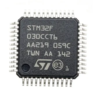
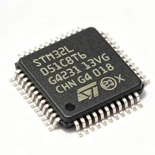
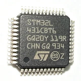
STM32F100C6T6B - 24MHz Cortex-M3 MCU 32KB LQFP-48 | STMicroelectronics
料号: STM32F100C6T6B ✓ 量产中| 数量 | 单价 | 小计 |
|---|---|---|
| 1 | $3.85 | $3.85 |
| 10 | $3.42 | $34.20 |
| 100 | $2.74 | $274.00 |
| 500 | $2.31 | $1,155.00 |
| 1,000 | $1.96 | $1,960.00 |
| 2,500 | $1.62 | $4,050.00 |
STM32F100C6T6B 概述
A microcontroller (MCU) is a single-chip computer containing a processor core, program memory (Flash), working memory (SRAM), and a rich peripheral mix including timers, ADCs, communication interfaces, and GPIO. Within the broader category hierarchy, the STM32F100 sits at Microcontroller -> ARM Cortex-M MCU -> 32-bit MCU -> Embedded Processor -> Semiconductor. Cortex-M3 cores implement the ARMv7-M architecture with Thumb-2 instruction set, deterministic interrupt handling, and hardware division — making them well suited to real-time control tasks.
Key features of the STM32F100C6T6B include a 12-bit ADC (1 µs conversion), two 12-bit DACs, six general-purpose 16-bit timers, a 24 MHz maximum core clock, and up to 37 GPIO pins. The device integrates up to eight communication interfaces including I2C, SPI, USART, and CAN, plus a 1-channel advanced timer for motor control. Operating voltage spans 2.0 V to 3.6 V across the –40 °C to +85 °C industrial temperature range.
Architecturally, the part uses ST's 130 nm CMOS process with embedded Flash and a nested vector interrupt controller (NVIC) capable of handling up to 60 maskable interrupt sources. The integrated voltage regulator supports both run, sleep, stop, and standby low-power modes. Hardware CRC and 96-bit unique device ID reduce firmware overhead and enable secure identification.
Typical applications include home appliances and white goods, HVAC control, motor control for low-voltage DC and stepper motors, industrial sensors, USB accessories, and low-cost consumer electronics such as remote controls, toys, and LED lighting controllers. The wide peripheral mix also makes the STM32F100C6T6B suitable for smart-metering peripherals and simple HMI boards.
When designing with this part, note that the 48-pin LQFP footprint is shared across much of the STM32F1 family, allowing straightforward migration to higher-density parts (C8/CB) without PCB redesign. Ensure the BOOT0 strap and NRST reset network follow ST's reference design, and respect the 3.3 V supply tolerance for reliable Flash operation.
This page synthesizes distributor pricing, drop-in LQFP-48 alternatives, and practical design notes not found in the standalone manufacturer datasheet.
直接替换替代料: STM32F100C6T6B ——相同封装,引脚兼容。需要 PCB 改动的不同封装料号已排除。
本系列中的变体
可与以下型号直接替换的同系列型号: STM32F100C6T6B (相同外形与封装尺寸) ——差异在于 Flash Memory, Package, SRAM, Timers.
快速对比工具——选择替代料号进行并排对比:
STM32F100C8T6B
✅ 直接替换📋 参考替代料(不在目录中)
STM32F100CBT6B
✅ 直接替换📋 参考替代料(不在目录中)
STM32F101C6T6A
✅ 直接替换 ⚠️ 规格未核验📋 参考替代料(不在目录中)
STM32F102C6T6
✅ 直接替换 ⚠️ 规格未核验📋 参考替代料(不在目录中)
STM32F103C6T6
✅ 直接替换 ⚠️ 规格未核验✓ 有现货
$2.05 / 个
查看数据手册 →STM32F100C6T6B 最大额定值与电气特性
| Core | ARM Cortex-M3 32-bit RISC |
| 最大时钟频率 | 24 MHz |
| Flash Memory | 32 KB |
| SRAM | 4 KB |
| Operating Voltage | 2.0 V to 3.6 V |
| 封装 | LQFP-48 (7x7 mm) |
| 引脚数量 | 48 |
| 安装类型 | Surface Mount |
| 工作温度 | -40 C to +85 C |
| GPIO Count | Up to 37 |
| ADC | 1x 12-bit, up to 10 channels (1 us conversion) |
| DAC | 2x 12-bit |
| Timers | 6x general-purpose 16-bit, 1x advanced-control (PWM) |
| Communication Interfaces | Up to 8 (I2C, SPI, USART, CAN) |
| MSL 等级 | 3 (168 hours) |
| RoHS 状态 | Compliant |
STM32F100C6T6B 引脚配置
| 引脚 1 | VBAT — Battery input for RTC domain |
| 引脚 2 | PC13 — GPIO/Tamper-RTC |
| 引脚 3 | PC14 — GPIO/OSC32_IN |
| 引脚 4 | PC15 — GPIO/OSC32_OUT |
| 引脚 5 | OSC_IN — External clock input |
| 引脚 6 | OSC_OUT — External clock output |
| 引脚 7 | NRST — Reset (active-low) |
| 引脚 8 | VSSA — Analog ground |
| 引脚 9 | VDDA — Analog supply |
| 引脚 10 | PA0 — GPIO/ADC_IN0/WKUP |
| 引脚 11 | PA1 — GPIO/ADC_IN1 |
| 引脚 12 | PA2 — GPIO/USART2_TX |
| 引脚 13 | PA3 — GPIO/USART2_RX |
| 引脚 14 | PA4 — GPIO/SPI1_NSS/DAC12 |
| 引脚 15 | PA5 — GPIO/SPI1_SCK/DAC1 |
| 引脚 16 | PA6 — GPIO/SPI1_MISO/ADC_IN6 |
| 引脚 17 | PA7 — GPIO/SPI1_MOSI/ADC_IN7 |
| 引脚 18 | PB0 — GPIO/ADC_IN8 |
| 引脚 19 | PB1 — GPIO/ADC_IN9 |
| 引脚 20 | PB2 — GPIO/BOOT1 |
| 引脚 21 | PB10 — GPIO/I2C2_SCL/USART3_TX |
| 引脚 22 | PB11 — GPIO/I2C2_SDA/USART3_RX |
| 引脚 23 | VSS_1 — Digital ground |
| 引脚 24 | VDD_1 — Digital supply |
| 引脚 25 | PB12 — GPIO/SPI2_NSS |
| 引脚 26 | PB13 — GPIO/SPI2_SCK |
| 引脚 27 | PB14 — GPIO/SPI2_MISO |
| 引脚 28 | PB15 — GPIO/SPI2_MOSI |
| 引脚 29 | PA8 — GPIO/TIM1_CH1 |
| 引脚 30 | PA9 — GPIO/USART1_TX/TIM1_CH2 |
| 引脚 31 | PA10 — GPIO/USART1_RX/TIM1_CH3 |
| 引脚 32 | PA11 — GPIO/USART1_CTS/TIM1_CH4 |
| 引脚 33 | PA12 — GPIO/USART1_RTS |
| 引脚 34 | PA13 — GPIO/SWDIO |
| 引脚 35 | VSS_2 — Digital ground |
| 引脚 36 | VDD_2 — Digital supply |
| 引脚 37 | PA14 — GPIO/SWCLK |
| 引脚 38 | PA15 — GPIO/SPI3_NSS |
| 引脚 39 | PB3 — GPIO/SPI3_SCK |
| 引脚 40 | PB4 — GPIO/SPI3_MISO |
| 引脚 41 | PB5 — GPIO/SPI3_MOSI |
| 引脚 42 | PB6 — GPIO/I2C1_SCL |
| 引脚 43 | PB7 — GPIO/I2C1_SDA |
| 引脚 44 | BOOT0 — Boot mode select |
| 引脚 45 | PB8 — GPIO/TIM4_CH1 |
| 引脚 46 | PB9 — GPIO/TIM4_CH2 |
| 引脚 47 | VSS_3 — Digital ground |
| 引脚 48 | VDD_3 — Digital supply |
典型应用
STM32F100C6T6B 适用于 7 应用s: Home Appliance Control, HVAC Fan and Blower Control, Industrial Sensor Nodes, Low-Cost LED Lighting Controllers, USB Accessories (via F101 and similar), Smart Metering Peripherals, Toys and Consumer Electronics.
Home Appliance Control
The STM32F100C6T6B's 24 MHz Cortex-M3 core, 12-bit ADC, and 16-bit advanced-control timer TIM1 suit washing machines, microwave ovens, and induction cooktops. The 48-pin LQFP exposes enough GPIO for keypad scanning, triac control, and LED status, while the 32 KB Flash holds motor-state and user-interface firmware. Six 16-bit timers drive PWM outputs at the 24 MHz core rate, adequate for low-frequency triac-based heater regulation; this 24 MHz bandwidth is exactly why ST positioned the F100 as the value-line for white goods.
推荐
HVAC Fan and Blower Control
BLDC and brushed-DC fans require closed-loop PWM control with back-EMF sensing; the STM32F100C6T6B's TIM1 advanced-control timer provides complementary PWM with dead-time insertion and a 1 µs ADC for current feedback. The 32 KB Flash holds PI/PID firmware and lookup tables, while 4 KB SRAM is enough for sensor fusion. Compared with the F103, the F100's 24 MHz clock trades DSP headroom for lower BOM cost; this part wins when the controller loops below 10 kHz.
推荐
Industrial Sensor Nodes
Industrial 4-20 mA loop-powered sensors benefit from the STM32F100C6T6B's 2.0-3.6 V wide supply and –40 °C to +85 °C industrial temperature range. The Cortex-M3 core handles Modbus RTU framing over USART, while 32 KB Flash stores calibration coefficients and 4 KB SRAM buffers samples. The 12-bit ADC and DAC combination enables analog sensor trimming in the field. The 24 MHz core is intentionally down-clocked vs the F103 to save quiescent current for loop-powered designs.
推荐
Low-Cost LED Lighting Controllers
DMX-512 and DALI LED drivers use the STM32F100C6T6B's USART for protocol framing and TIM1 PWM for smooth dimming. The 12-bit DAC sets constant-current references for analog dimming fallback. With 32 KB Flash, the firmware fits DMX/DALI stacks plus color-temperature curves. This part's lower 24 MHz ceiling is rarely a limitation for lighting loops, and the F100 value-line pricing keeps 4-channel RGBW fixtures under BOM targets.
推荐
USB Accessories (via F101 and similar)
Although the STM32F100C6T6B itself lacks USB, the value-line family is commonly deployed alongside USB-serial bridges. The 48-pin LQFP exposes the USARTs needed for CDC-class bridges and the timers for HID-class button reporting. STM32F102 (USB-found 48 pin variant) shares the same footprint and is often co-deployed. The F100 remains attractive as a slave processor that offloads USB stacks from the host MCU; firmware migration to STM32F102 is one register change.
推荐
Smart Metering Peripherals
Electricity, gas, and heat meters use the STM32F100C6T6B's 12-bit ADC for voltage and current sensing plus the integrated RTC for time-stamping. The 4 KB SRAM buffers interval data while 32 KB Flash stores tariff tables. ST's value-line positioning targets sub-2-USD BOMs at qty 1k, a key cost target for utility-grade meters. The 24 MHz core is adequate for IEC 62056-21 protocol stacks and 100 Hz sample rates on metrology ADCs.
推荐
Toys and Consumer Electronics
Battery-powered toys, remote-controlled devices, and educational electronics use the STM32F100C6T6B for its low active current at 24 MHz and rich timer set. Six 16-bit timers drive servo, motor, and audio PWM channels; 4 KB SRAM holds small audio buffers; and 32 KB Flash fits simple games and UI flows. The 2.0 V minimum supply allows direct Li-Ion or 2x AA operation, simplifying battery use cases where a single-cell Li-Ion or 2x AA pack is the source.
推荐
推荐产品汇总
工程参考数据: STM32F100C6T6B ——对比、设计指导和合规信息。
选型指南
与替代料对比
| 参数 | 本产品 | STM32F100C8T6B | STM32F100CBT6B | STM32F101C6T6A | STM32F102C6T6 | STM32F103C6T6 |
|---|---|---|---|---|---|---|
| Brand | STMicroelectronics | STMicroelectronics | STMicroelectronics | STMicroelectronics | STMicroelectronics | STMicroelectronics |
| Package | LQFP-48 (7x7 mm) | LQFP-48 (7x7 mm) - same | LQFP-48 (7x7 mm) - same | LQFP-48 (7x7 mm) - same | LQFP-48 (7x7 mm) - same | LQFP-48 (7x7 mm) - same |
| Core | ARM Cortex-M3 | ARM Cortex-M3 | ARM Cortex-M3 | ARM Cortex-M3 | ARM Cortex-M3 | ARM Cortex-M3 |
| Maximum Clock | 24 MHz | 24 MHz - same | 24 MHz - same | 36 MHz - +50% | 48 MHz - +100% | 72 MHz - +200% |
| Flash Memory | 32 KB | 64 KB - +100% | 128 KB - +300% | 32 KB - same | 32 KB - same | 32 KB - same |
| SRAM | 4 KB | 8 KB - +100% | 8 KB - +100% | 6 KB - +50% | 4 KB - same | 10 KB - +150% |
| USB | No | No | No | No | USB FS - added | USB FS - added |
| CAN | Yes (bxCAN) | Yes - same | Yes - same | Yes - same | No - removed | Yes - same |
关键差异点
- Lowest-cost STM32F1 LQFP-48 with Cortex-M3 at 24 MHz (对比 STM32F103C6T6)
- Migration path to 64 KB and 128 KB Flash on same footprint (对比 GD32F130C6T6 (cross-brand))
- Higher-density STM32F102 migration adds integrated USB (对比 STM32F103C6T6)
设计说明
The STM32F100C6T6B integrates a 1.8 V LDO regulator from the 2.0-3.6 V VDD supply. Decouple each VDD pin (1, 24, 36, 48) with a 100 nF ceramic capacitor placed within 5 mm of the pin, and add a bulk 4.7 uF tantalum or ceramic on the main 3.3 V rail. VDDA must be tied to VDD with an LC filter (10 ohm + 100 nF) to keep ADC noise below 1 LSB; VSSA ties directly to the ground plane.
BOOT0 must be tied to ground through a 10 kohm resistor for normal Flash execution; leaving it floating causes intermittent boot failures when noise couples to the pin. The NRST line needs a 10 kohm pull-up and a 100 nF capacitor to VSS for proper reset - omitting these causes brown-out instability. For SWD debugging, expose PA13 (SWDIO) and PA14 (SWCLK) on the PCB even if not populated, so future debug access is possible without board rework.
Route the crystal traces (OSC_IN/OSC_OUT) as short as possible, symmetric in length, and guard-trace with a ground pour. Place the load capacitors (typically 15 pF for 8 MHz HSE) within 2-3 mm of the pins. The 48-pin LQFP has 0.5 mm pitch, which is hand-solderable with a fine tip but requires a reflow profile per JEDEC J-STD-020 (peak 245 C for SnAgCu). Use at least 6 ground pins as thermal vias to a continuous ground plane for STM32 thermal performance.
The STM32F100C6T6B's GPIO toggles at speeds up to 18 MHz; for SPI signals above 9 MHz, add 33 ohm series damping resistors near the MCU to suppress reflections on traces longer than 25 mm. Keep analog ADC inputs (PA0-PA7, PB0-PB1) physically separated from switching signals (PWM outputs on PA8-PA12) on different ground islands joined at the MCU's VSSA pin to avoid digital switching noise coupling into ADC measurements.
合规信息
RoHS compliant per ST product page. Not AEC-Q100 qualified - choose STM32F100 automotive-grade variant (R6T6B) for automotive use.