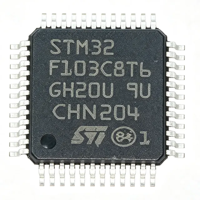
STM32F103C8T6 - 72MHz Cortex-M3 MCU,64KB Flash,LQFP-48 | STMicroelectronics
料号: STM32F103C8T6 ✓ 量产中| 数量 | 单价 | 小计 |
|---|---|---|
| 1 | $3.1 | $3.10 |
| 10 | $2.78 | $27.80 |
| 100 | $2.45 | $245.00 |
| 500 | $2.18 | $1,090.00 |
| 1,000 | $1.92 | $1,920.00 |
| 3,000 | $1.68 | $5,040.00 |
STM32F103C8T6 概述
ARM Cortex-M3 微控制器(MCU)是由 Arm Holdings 设计的 32 位 RISC 处理器内核,适用于需要低功耗确定性实时性能的嵌入式应用。Cortex-M3 位于 Cortex-M 系列的低端(高于 Cortex-M0/M0+,低于 Cortex-M4/M7),该类别中的微控制器将处理器内核与片上存储器、外设和模拟模块集成到单个系统级芯片中。STM32F103 系列具体属于更广泛的层级:ARM Cortex-M3 -> 32 位 MCU -> STM32F1 系列 -> STM32 主流系列 -> STMicroelectronics 微控制器 -> 半导体。这一层级很重要,因为它决定了工具链(Arm Cortex-M3 支持标准的 Arm Keil、IAR、GCC 和 STM32CubeIDE 流程)以及整个 STM32 平台使用的外设编程模型。
主要特性包括 64 KB 嵌入式 Flash(具有边读边写能力)、20 KB SRAM、2.0 V 至 3.6 V 电源范围、8 MHz 内部 RC 振荡器(通过 PLL 倍频至 72 MHz)、两个 12 位 ADC(1 µs 转换,最多 16 通道)、七个 16 位定时器以及一个全速 USB 2.0 全速设备/主机/OTG 控制器。通信外设包括三个 USART、两个 SPI(18 Mbit/s)、两个 I2C 总线(400 kHz)、一个 CAN 2.0B 接口和一个 USB 全速端口。48 引脚 LQFP 封装提供 37 个 5 V 耐压 GPIO 引脚。
在架构上,Cortex-M3 内核每 MHz 提供 1.25 Dhrystone MIPS,支持 Thumb-2 指令集,并包含具有可配置优先级和硬件堆栈处理的嵌套向量中断控制器(NVIC)。集成稳压器和欠压复位(BOR)简化了电源设计,而带有篡改检测引脚的 4 字节备份寄存器支持电池供电的 RTC 模式。
典型应用包括工业控制板、电机驱动(BLDC/PMSM FOC 补充)、USB HID/COM 端口设备、CAN 总线节点接口以及低成本开发平台,例如著名的“Blue Pill”板。
使用此器件进行设计时,请将 100 nF 陶瓷去耦电容尽可能靠近每个 VDD/VDDA 引脚对放置,并为 NRST 引脚连接保留 10 kΩ 上拉电阻和可选复位按钮。确保每次上电时 BOOT0 引脚状态与所需的启动存储器匹配。
本页面综合了分销商定价、直接替代方案(首先同品牌 STM32F103 变体,然后跨品牌引脚兼容部件)以及制造商数据表中未包含的实用设计说明。
直接替换替代料: STM32F103C8T6 ——相同封装,引脚兼容。需要 PCB 改动的不同封装料号已排除。
快速对比工具——选择替代料号进行并排对比:
STM32F103CBT6
✓ 有现货
$3.2 / 个
查看数据手册 →STM32F030C8T6
✓ 有现货
$0.98 / 个
查看数据手册 →STM32F103C8T7
📋 参考替代料(不在目录中)
GD32F103C8T6
📋 参考替代料(不在目录中)
APM32F103C8T6
📋 参考替代料(不在目录中)
STM32F103C8T6 最大额定值与电气特性
| Core Architecture | ARM Cortex-M3 (32-bit RISC) |
| 最大时钟频率 | 72 MHz |
| Flash Memory | 64 KB |
| SRAM | 20 KB |
| Supply Voltage (VDD) | 2.0 V to 3.6 V |
| 封装 | LQFP-48 (7x7 mm, 0.5 mm pitch) |
| GPIO Count | 37 |
| ADC | 2x 12-bit, 1 µs, up to 16 channels |
| Timers | 7x 16-bit (including 1x watchdog, 2x SysTick) |
| USART | 3 |
| SPI | 2 (18 Mbit/s) |
| I2C | 2 (400 kHz) |
| USB | 1x USB 2.0 Full-Speed device/host/OTG |
| CAN | 1x CAN 2.0B |
| 工作温度 | -40 °C to +85 °C (industrial grade) |
| RoHS 状态 | Compliant |
STM32F103C8T6 引脚配置
| 引脚 1 | VBAT — Backup battery supply input |
| 引脚 2 | PC13 — GPIO PC13, anti-tamper (RTC) |
| 引脚 3 | PC14 — GPIO PC14 / OSC32_IN |
| 引脚 4 | PC15 — GPIO PC15 / OSC32_OUT |
| 引脚 5 | OSC_IN — HSE oscillator input |
| 引脚 6 | OSC_OUT — HSE oscillator output |
| 引脚 7 | NRST — Reset input, active-low |
| 引脚 8 | VSSA — Analog ground |
| 引脚 9 | VDDA — Analog supply (2.4 V - 3.6 V) |
| 引脚 10 | PA0 — GPIO PA0 / WKUP / ADC_IN0 / TIM2_CH1 |
| 引脚 11 | PA1 — GPIO PA1 / ADC_IN1 / TIM2_CH2 |
| 引脚 12 | PA2 — GPIO PA2 / USART2_TX / ADC_IN2 |
| 引脚 13 | PA3 — GPIO PA3 / USART2_RX / ADC_IN3 |
| 引脚 14 | PA4 — GPIO PA4 / SPI1_NSS / ADC_IN4 |
| 引脚 15 | PA5 — GPIO PA5 / SPI1_SCK / ADC_IN5 |
| 引脚 16 | PA6 — GPIO PA6 / SPI1_MISO / ADC_IN6 |
| 引脚 17 | PA7 — GPIO PA7 / SPI1_MOSI / ADC_IN7 |
| 引脚 18 | PB0 — GPIO PB0 / ADC_IN8 / TIM3_CH3 |
| 引脚 19 | PB1 — GPIO PB1 / ADC_IN9 / TIM3_CH4 |
| 引脚 20 | PB2 — GPIO PB2 / BOOT1 (also PB-BOOT input) |
| 引脚 21 | PB10 — GPIO PB10 / I2C2_SCL / USART3_TX |
| 引脚 22 | PB11 — GPIO PB11 / I2C2_SDA / USART3_RX |
| 引脚 23 | VSS_1 — Digital ground |
| 引脚 24 | VDD_1 — Digital supply (2.0 V - 3.6 V) |
| 引脚 25 | PB12 — GPIO PB12 / SPI2_NSS / CAN2_RX |
| 引脚 26 | PB13 — GPIO PB13 / SPI2_SCK / CAN2_TX / USB_DP pull-up |
| 引脚 27 | PB14 — GPIO PB14 / SPI2_MISO |
| 引脚 28 | PB15 — GPIO PB15 / SPI2_MOSI |
| 引脚 29 | PA8 — GPIO PA8 / USART1_CK / TIM1_CH1 |
| 引脚 30 | PA9 — GPIO PA9 / USART1_TX / TIM1_CH2 |
| 引脚 31 | PA10 — GPIO PA10 / USART1_RX / TIM1_CH3 |
| 引脚 32 | PA11 — GPIO PA11 / CAN1_RX / USBDM (USB data minus) |
| 引脚 33 | PA12 — GPIO PA12 / CAN1_TX / USBDP (USB data plus) |
| 引脚 34 | PA13 — GPIO PA13 / JTMS / SWDIO |
| 引脚 35 | VSS_2 — Digital ground |
| 引脚 36 | VDD_2 — Digital supply (2.0 V - 3.6 V) |
| 引脚 37 | PA14 — GPIO PA14 / JTCK / SWCLK |
| 引脚 38 | PA15 — GPIO PA15 / JTDI |
| 引脚 39 | PB3 — GPIO PB3 / JTDO / TRACESWO |
| 引脚 40 | PB4 — GPIO PB4 / JNTRST |
| 引脚 41 | PB5 — GPIO PB5 / I2C1_SMBAI |
| 引脚 42 | PB6 — GPIO PB6 / I2C1_SCL / TIM4_CH1 |
| 引脚 43 | PB7 — GPIO PB7 / I2C1_SDA / TIM4_CH2 |
| 引脚 44 | BOOT0 — Boot mode select (0 = Flash, 1 = System bootloader) |
| 引脚 45 | PB8 — GPIO PB8 / TIM4_CH3 |
| 引脚 46 | PB9 — GPIO PB9 / TIM4_CH4 |
| 引脚 47 | VSS_3 — Digital ground |
| 引脚 48 | VDD_3 — Digital supply (2.0 V - 3.6 V) |
典型应用
STM32F103C8T6 适用于 6 应用s: Industrial Control Boards, USB HID / Virtual COM Port Devices, BLDC / PMSM Motor Drives, CAN-Bus Node Interface, Low-Cost Development Platforms ("Blue Pill"), IoT Sensor / Smart Home Edge Nodes.
Industrial Control Boards
The STM32F103C8T6 fits industrial control boards because its 72 MHz Cortex-M3 core and 64 KB Flash comfortably handle Modbus RTU slave firmware, PID loop control, and user-interface logic on a single chip. The dual 12-bit ADCs (1 µs, up to 16 channels) sample 4-20 mA sensor inputs at the kHz rates typical of PLC analog modules, while the three USARTs (USART1/2/3) support simultaneous RS-232/RS-485 fieldbus and a debug console. The 2.0 V to 3.6 V supply range aligns with 3.3 V industrial backplanes, and the -40 °C to +85 °C operating temperature meets most cabinet-mounted equipment specs. On-board CAN 2.0B lets a single MCU handle both a sensor bus and an external CANopen master.
推荐
USB HID / Virtual COM Port Devices
The STM32F103C8T6's integrated USB 2.0 Full-Speed device controller (12 Mbit/s) makes it a natural fit for USB HID-class peripherals, virtual COM-port bridges, and CDC-MSC composite devices without external PHY hardware. The 72 MHz core and 20 KB SRAM execute the standard ST USB device library (and STM32CubeMX-generated middleware) with room left for application logic, while the 64 KB Flash fits typical HID report descriptors and command parsers. Its 2.0 V to 3.6 V rail tolerance lets designers tap the USB 5 V bus through an LDO and run the MCU from a single 3.3 V supply. Designers should add ESD protection (USBLC6-2SC6) and a 1.5 kΩ pull-up on the D+ line to the USB connector.
推荐
BLDC / PMSM Motor Drives
The STM32F103C8T6 is widely used in sensorless or hall-sensored BLDC and PMSM motor drives for low- to mid-power applications (fans, pumps, e-bike hubs). Its 72 MHz Cortex-M3 plus advanced timers (TIM1 with complementary PWM and dead-time insertion) generate the 6-step or space-vector PWM that drives a 3-phase inverter at up to tens of kHz switching. The two ADCs trigger from timer events to sample phase currents within the PWM cycle for low-latency commutation, and the quadrature encoder interface on TIM2 supports sensored FOC firmware patterns. CAN bus readiness lets the drive communicate with a central PLC, while the 2.0-3.6 V range accepts a wide range of bus-powered motor-control supplies.
推荐
CAN-Bus Node Interface
The STM32F103C8T6 is a battle-tested choice for CAN 2.0B node interfaces used in automotive body-electronics, industrial CANopen, and medical device buses. The bxCAN peripheral supports standard and extended frames with hardware filter banks and a 1 Mbit/s bit rate suitable for most fieldbus deployments. With 64 KB Flash the device holds small CANopen/CANFestival stacks and application logic, while three USARTs allow a companion GPS or HMI link. Operating temperature of -40 °C to +85 °C suits non-automotive nodes; designers needing AEC-Q100 should select the STM32F103C8T7 variant. Drop a 60 Ω termination resistor only on the bus ends and add a TJA1050 or TCAN332 transceiver externally.
推荐
Low-Cost Development Platforms ("Blue Pill")
The STM32F103C8T6 is the headline MCU of the iconic "Blue Pill" development board that became the de-facto entry ticket to ARM Cortex-M3 firmware development. Its 72 MHz core, 64 KB Flash, SWD debug pins, USB connector, and 48-pin LQFP form factor fit on a 53 x 23 mm PCB with a USB micro-B port, a 3.3 V LDO, a reset button, and boot-mode jumpers. Students and hobbyists target it with STM32CubeIDE, PlatformIO, and the Arduino STM32 core, and any prototype firmware written on the Blue Pill ports directly to custom hardware when the same MCU is kept on the production board. The LQFP-48 footprint is also shared by several GD32 and APM32 pin-compatibles, simplifying second sourcing for educational kits.
推荐
IoT Sensor / Smart Home Edge Nodes
The STM32F103C8T6 handles Smart Home and IoT edge nodes that need local sensor aggregation, BLE/Wi-Fi module handshaking, and OTA bootloading without committing to a high-cost M4-class part. Three USARTs (USART1/2/3) drive an ESP-01 Wi-Fi co-processor, a GPS module, and a debug console in parallel; two SPIs (up to 18 Mbit/s) talk to a LoRa SX1278 or a small TFT display; two I2C buses serve a BME280 environmental sensor and an OLED panel. The 12-bit ADC samples analog sensors such as soil-moisture probes, and the RTC plus 4-byte backup register keep a wall-clock time across deep-sleep cycles powered by a CR2032. The 2.0-3.6 V supply range supports direct lithium-ion battery operation via an LDO or buck.
推荐
推荐产品汇总
工程参考数据: STM32F103C8T6 ——对比、设计指导和合规信息。
选型指南
与替代料对比
| 参数 | 本产品 | STM32F103CBT6 | STM32F103C8T7 | GD32F103C8T6 | APM32F103C8T6 | STM32F030C8T6 |
|---|---|---|---|---|---|---|
| Brand | STMicroelectronics | STMicroelectronics | STMicroelectronics | GigaDevice | GigaDevice | STMicroelectronics |
| Package | LQFP-48 (7x7 mm) | LQFP-48 (7x7 mm) - same | LQFP-48 (7x7 mm) - same | LQFP-48 (7x7 mm) - same | LQFP-48 (7x7 mm) - same | LQFP-48 (7x7 mm) - same |
| Core | ARM Cortex-M3 | ARM Cortex-M3 | ARM Cortex-M3 | ARM Cortex-M3 | ARM Cortex-M3 | ARM Cortex-M0 (-1 class) |
| Max Clock | 72 MHz | 72 MHz | 72 MHz | 108 MHz (+50%) | 96 MHz (+33%) | 48 MHz (-33%) |
| Flash | 64 KB | 128 KB (+100%) | 64 KB | 64 KB | 64 KB | 64 KB |
| SRAM | 20 KB | 20 KB | 20 KB | 20 KB | 20 KB | 8 KB (-60%) |
| USB | USB 2.0 Full-Speed | USB 2.0 Full-Speed | USB 2.0 Full-Speed | USB 2.0 Full-Speed | USB 2.0 Full-Speed | No USB |
| CAN | 1x CAN 2.0B | 1x CAN 2.0B | 1x CAN 2.0B | 1x CAN 2.0B | 1x CAN 2.0B | No CAN |
| Automotive Grade | No (industrial -40/+85C) | No | Yes (AEC-Q100) | No | No | No |
关键差异点
- 同系列内引脚兼容的 Flash 翻倍直接替代 (对比 STM32F103CBT6)
- 相同硅片/裸片上提供 AEC-Q100 汽车温度等级 (对比 STM32F103C8T7)
- 相同 LQFP-48 封装上快两到四倍的内核 (对比 GD32F103C8T6)
设计说明
将 100 nF 陶瓷去耦电容尽可能靠近每个 VDD/VDDA 引脚对(引脚 24、36、48 / 9)放置,并在主 3.3 V 电源轨上 20 mm 内至少放置一个 4.7 µF 大容量电容。VDDA 需要低阻抗连接;如果主 3.3 V 电源有噪声,请在 VDD 和 VDDA 之间插入铁氧体磁珠。如果不使用备用电池,请将 VBAT 连接到 VDD。上电时始终将 BOOT0 引脚保持低电平,以默认从 Flash 启动。
将 8 MHz HSE 晶体走线布置得短且对称,晶体放置在距 OSC_IN/OSC_OUT(引脚 5/6)5 mm 以内,负载电容(通常 20-30 pF)直接在晶体外壳处接地。保持 USB D+/D-(PA11/PA12)长度匹配(目标差值 <2 mm),并将 D+ 上的 1.5 kΩ 上拉电阻放在连接器旁边,而不是 MCU 侧。为 NRST 提供 10 kΩ 上拉电阻,并通过复位按钮提供到 GND 的低阻抗路径。
使用 CAN 或 USB 时,请在连接器附近添加 TVS 二极管阵列,如 USBLC6-2SC6 或 PESD1CAN,以满足 IEC 61000-4-2 ±8 kV 空气放电和 ±4 kV 接触放电等级。USB D+(PA12)的内部上拉不足以实现可靠枚举;建议使用外部 1.5 kΩ 电阻连接到 3.3 V。CAN 总线终端应仅在两端使用 120 Ω,并在多节点线束中使用分裂电容网络抑制短截线。
不要将 BOOT0 悬空——上电期间该引脚上的噪声会间歇性地将 MCU 启动到系统引导加载程序,应用程序代码将看起来缺失。三个常见错误:(1)将 VBAT 悬空而不是连接到 VDD,这会为内部二极管充电并破坏备份寄存器写入;(2)将 PA13/PA14 用作 GPIO 而未禁用 JTAG/SWD,因为复位后 JTAG 默认使用这些引脚;(3)在 I2C 引脚上将 GPIO 输出速度配置为“50 MHz”,这会导致振铃——始终选择“2 MHz”开漏并配合外部上拉电阻。
合规信息
RoHS-compliant per ST product page; AEC-Q100 grade is a separate SKU (STM32F103C8T7). Halogen-free status not explicitly verified in the provided data and flagged as 'unknown'.







