FPGA & CPLD
Products (6358)

EP1K100FC256-3N - ACEX 1K FPGA 100K Gates | Altera
The Altera EP1K100FC256-3N is a 2.5 V ACEX 1K field-programmable gate array (FPGA) that provides 4,992 logic elements, 49,152 RAM bits, 624 LABs, and 186 user I/Os in a 256-ball FBGA package. It is commonly described as a 100K-gate device for data-path, DSP, and register-intensive logic. The -3 suffix identifies the commercial speed grade; the N suffix indicates lead-free package finish. As a legacy Altera/Intel part, it is still stocked by leading distributors as of 2026-09-06. An FPGA is a semiconductor device containing programmable logic blocks and programmable interconnects that can implement arbitrary digital logic after manufacture. The ACEX 1K architecture combines look-up table LUT-based logic with embedded array blocks EABs, allowing designers to create state machines, data-path controllers, and memory functions in one device. This product sits between simple CPLDs and high-density modern FPGAs; it is suited to moderate gate-count systems that need reprogrammable hardware without the cost and complexity of application-specific integrated circuits. Key features of the EP1K100FC256-3N include 624 LABs organized into 4,992 logic elements, 49,152 bits of embedded RAM capable of ROM, RAM, dual-port RAM, or FIFO functions, and 186 user I/Os accessible from the 256-ball FineLine BGA package. The core operates at 2.5 V with a 0.22 um CMOS process, and the MultiVolt I/O interface lets designers connect different I/O bank voltages. The -3 commercial speed grade supports moderate system clocks, while the N suffix provides a lead-free package finish suitable for RoHS-oriented assembly flows. For architecture, ACEX 1K uses a die-efficient LUT fabric combined with EABs. Each LAB brings local routing to form fast carry chains for arithmetic and DSP functions; EABs are true dual-port structures that can store coefficients, form FIFOs, or split into shorter word widths. The PCI pull-up clamp diode, slew-rate control, and open-drain output options described in the Altera datasheet are set pin-by-pin through Altera software logic options. This makes the device particularly practical for legacy bus interfacing and custom logic integration where extra discretes would otherwise be required. Typical applications include digital signal processing front ends, telecommunications line-card bridging, industrial machine-control glue logic, medical instrumentation timing, and audio effects/DSP prototypes. The 186 user I/Os support wide parallel ADC/DAC buses and processor interfaces; the 49,152-RAM-bit EAB capacity reduces the need for external FIFOs and lookup tables. The 2.5 V core helps lower dynamic power compared to older 3.3 V programmable logic in high-frequency datapath designs. A key design consideration is configuration: ACEX 1K FPGAs require an external configuration device or download cable because they are SRAM-based and lose their program on power-off. Use an Altera EPC configuration PROM or download the bitstream at power-up, and confirm VCCINT decoupling and I/O voltage sequencing from the ACEX 1K datasheet before layout. As with all FPGAs, timing closure should come from the place-and-route timing report, not from distributor speed figures. This page adds value beyond the manufacturer datasheet by synthesizing distributor stock information, comparing pin-compatible ACEX speed-grade variants, and providing practical design guidance for legacy FPGA replacement planning. It is intended for engineers who are sourcing an obsolete-class component, validating a drop-in replacement, or reintroducing a legacy ACEX 1K design to production.

EP1K100FC484-1 - 100K Gate ACEX-1K FPGA, 484-BGA, 333MHz | Intel / Altera
The Intel / Altera EP1K100FC484-1 is an ACEX-1K family Field-Programmable Gate Array (FPGA) integrating 100,000 gates, 4,992 logic cells (LEs), and 49,152 RAM bits in a 484-ball FineLine BGA (FBGA) package. It is built on a 0.22 µm CMOS process, operates from a 2.5 V core supply, supports user I/O voltages up to 3.3 V, and runs internal logic at up to 333 MHz. The '-1' speed grade designates the slowest commercial grade in the ACEX-1K family. An FPGA (Field-Programmable Gate Array) is a programmable logic device that lets engineers implement arbitrary digital logic, memory blocks, and I/O functions on a single chip after PCB fabrication. Within the wider programmable-logic taxonomy, ACEX-1K belongs to the SRAM-look-up-table-based FPGA category, which sits between low-density CPLDs and high-density Stratix-class FPGAs. The ACEX-1K family was Altera's mid-density, cost-optimized line, offering embedded array blocks (EABs) for RAM/ROM and a look-up-table (LUT) fabric for combinatorial and registered functions. Key features of the EP1K100FC484-1 include 333 user I/O pins, six embedded array blocks providing up to 49 Kbits of dual-port RAM, a 4-input LUT-based logic element, in-system programmability via an IEEE 1149.1 JTAG interface, and on-chip pull-up resistors. The device supports hot-socketing, multi-voltage I/O standards including LVTTL, LVCMOS, PCI, and SSTL, and provides built-in clock-management with dedicated clock input pins feeding internal global routing networks. Architecturally, the EP1K100FC484-1 implements an enhanced embedded array that combines dedicated memory blocks (EABs) with a logic array for high-density megafunctions such as FIFOs, CAMs, and multipliers. The 0.22 µm process and 2.5 V core provide a balance between logic density and static power consumption suitable for industrial glue logic, bus bridging, and DSP front-end functions. Typical applications include industrial control, telecommunications line-card glue logic, PCI bus interfaces, low-to-medium volume ASIC prototyping, and embedded DSP pre-processing. The 484-FBGA package supports high I/O count designs with controlled impedance signal integrity for backplane interfaces. When designing with the EP1K100FC484-1, ensure the Quartus II (or MAX+PLUS II) design tool targets the EP1K100 device and the FC484 package, and that the bank-by-bank VCCIO voltages match each I/O standard. Decoupling must follow the Altera reference design with 0.1 µF capacitors per power pin and bulk tantalum or ceramic on each supply rail. This page synthesizes distributor stock and pricing, drop-in alternatives, and practical design considerations that are not aggregated on the original Altera ACEX-1K datasheet - information gain built on top of the manufacturer's published specifications.
EP1K100FC484-1N - 100K Gate ACEX-1K FPGA 333 I/O 484-FBGA | Intel
The Intel EP1K100FC484-1N is a member of the ACEX-1K family of Field Programmable Gate Arrays (FPGAs), delivering 100,000 system gates and 4,992 logic elements in a 484-ball FineLine BGA package. It provides 49,152 bits of embedded SRAM organized as 4 EAB (Embedded Array Block) blocks, 624 LABs/CLBs, and 333 user I/O pins. The device operates from a 2.5 V core supply and is built on a 0.22 µm CMOS process supporting clock rates up to 333.33 MHz. A Field Programmable Gate Array (FPGA) is a type of integrated circuit containing an array of programmable logic blocks, interconnect, and I/O cells that the designer configures after manufacture. FPGAs sit in the broader hierarchy of programmable logic devices (PLDs) -> FPGAs -> SRAM-based FPGAs -> ACEX-1K family -> Intel (formerly Altera) programmable logic portfolio. They are used to implement custom digital logic, glue logic, state machines, DSP pipelines, and bus interfaces when an ASIC is too costly or when time-to-market is critical. Key features of the EP1K100FC484-1N include 333 user I/O pins (the largest I/O count available in the ACEX-1K 100K family), 49 Kbits of dual-port embedded SRAM, hot-socketing support, multi-voltage I/O (1.5 V, 1.8 V, 2.5 V, 3.3 V LVTTL/LVCMOS), 4 phase-locked loops, and JTAG-based in-system programmability via IEEE 1149.1 boundary scan. The device supports the Quartus II design toolchain (legacy) for synthesis, place-and-route, and bitstream generation. Architecturally, the ACEX-1K combines a fine-grained Logic Array Block (LAB) fabric with coarse-grained Embedded Array Blocks (EABs) for memory-intensive functions such as CAMs, RAMs, and ROMs. Each EAB can be configured as 4,096 bits of RAM and supports true dual-port operation. The I/O ring supports LVDS, SSTL, and GTL signaling in addition to standard LVTTL/LVCMOS, enabling direct interfacing with DDR SDRAM and high-speed backplane transceivers. Typical applications include telecom line cards, industrial data acquisition, networking routers, low-cost ASIC prototyping, and PCI bridge implementations. The wide I/O count also makes it suitable for video processing front-ends, custom peripheral controllers, and legacy system upgrades where 5 V-tolerant or multi-voltage translation is required. When designing with this device, note that the EP1K100FC484-1N is in the -1N speed grade (medium speed) and the commercial 0 °C to 70 °C operating range. Bitstream configuration requires a serial configuration EPROM (EPCS) or JTAG download. Multi-voltage I/O banks must each be supplied independently. This page synthesizes distributor pricing, same-brand drop-in alternatives within the ACEX-1K family, and practical FPGA design notes not found in the legacy Altera datasheet, including migration guidance to Cyclone-series devices for new designs.
EP1K100FC484-2 - 100K-Gate ACEX-1K FPGA, 484-BGA, 2.5V | Altera
The Altera EP1K100FC484-2 is a member of the ACEX-1K family of low‑cost, 2.5 V SRAM‑based FPGAs, delivering approximately 100,000 system gates, 4,992 logic elements, 49,152 bits of embedded dual‑port RAM, and 333 user I/O pins in a 484‑ball FineLine BGA package. It is fabricated on a 0.22 µm CMOS process and operates from a 2.5 V core supply with multi‑volt I/O support for 1.8 V, 2.5 V and 3.3 V interfaces. The -2 speed grade targets a maximum internal clock of 250 MHz, balancing density and timing margin for cost‑sensitive programmable logic designs. An FPGA (Field‑Programmable Gate Array) is a reprogrammable semiconductor device that lets engineers implement custom digital logic, memory blocks and arithmetic functions without the cost of an ASIC. Within the programmable logic hierarchy, the ACEX‑1K family belongs to the low‑cost CPLD‑replacement tier of SRAM‑based FPGAs, sitting between classic PLDs and higher‑density families such as APEX or Cyclone. Its architecture combines logic array blocks (LABs), embedded array blocks (EABs) for dual‑port RAM and ROM, and a continuous interconnect, which makes it suitable for glue‑logic, bus‑interface and DSP‑frontend functions. The EP1K100FC484-2 uses an enhanced embedded array with 624 LABs and 4,992 logic elements, supported by 49,152 RAM bits organized into EABs. Each EAB provides up to 4,096 RAM bits and is configurable as dual‑port RAM, ROM, or logic. Combined with multi‑volt I/O support, this enables seamless bridging between legacy 5 V tolerant buses and 3.3 V or 2.5 V processors. The 484‑BGA package exposes 333 user I/O pins, allowing wide parallel buses, multiple UARTs, and high‑pin‑count memory interfaces on a compact board footprint. Typical applications include telecommunications line cards, industrial control and factory‑automation controllers, low‑cost DSP preprocessing, peripheral bridges for PC/104 and VME systems, and high‑speed glue logic. Its 2.5 V core and on‑chip EAB memory make it well suited to data‑path and protocol‑conversion designs. Designers should note that this part is now in the Altera/Intel legacy lifecycle; long‑term availability is limited and the design should consider newer Cyclone or MAX families for new projects. When designing with the EP1K100FC484-2, place decoupling capacitors as close as possible to every VCCINT/VCCIO ball, follow the FineLine BGA fan‑out rules for a 1.0 mm pitch, and use the Quartus II design suite (legacy version supporting ACEX‑1K) for synthesis, place‑and‑route, and timing closure. This page synthesizes distributor pricing, same‑family drop‑in alternatives, and practical design notes not collected on any single manufacturer datasheet.
EP1K100FC484-2N - 100K Gates ACEX-1K FPGA 333 I/O 484-FBGA | Intel
The Intel (formerly Altera) EP1K100FC484-2N is a member of the ACEX-1K family of FPGAs integrating 100,000 system gates, 4,992 logic elements, and 49,152 bits of embedded array (EAB) memory in a 484-ball FineLine BGA package, with a speed grade of -2 (commercial, non-Lead-free). It offers 333 user I/O pins and is built on a 0.22 µm SRAM-based process running from a 2.5 V core supply with multi-voltage I/O support. An FPGA (Field-Programmable Gate Array) is a type of programmable logic device (PLD) containing an array of configurable logic blocks (CLBs), embedded memory blocks, and programmable interconnect, all defined by a user-loaded bitstream after manufacture. The ACEX-1K family sits within Intel's broader hierarchy of programmable logic: PLD -> CPLD/FPGA -> SRAM-based FPGA -> low-cost system-on-a-programmable-chip (SOPC) integration platform. Each logic element combines a 4-input look-up table, a programmable flip-flop, and a dedicated carry chain, while embedded array blocks (EABs) provide true dual-port RAM up to 16 bits wide. Key features include 100K typical gates (49,152 RAM bits), 333 maximum user I/O, 250 MHz internal performance, JTAG-based in-system programmability via the IEEE 1149.1 boundary-scan interface, and built-in support for LVTTL, LVCMOS, PCI, SSTL-2/3, and GTL+ I/O standards. The -2 speed grade places this part in the mid-speed tier of the family, faster than -3 but slower than -1. The ACEX-1K architecture provides enhanced embedded arrays for implementing megafunctions such as efficient memory and specialized peripheral interfaces. A fast continuous interconnect structure called the MultiCore architecture routes signals efficiently across the device, and dedicated clock pins feed global clock networks with low skew. Typical applications include telecommunications glue logic, industrial control and instrumentation, low-cost glue logic for ASIC prototyping, video and image processing front-ends, network routers, and PCI bridge designs. The 333 I/O count makes it well suited to bus-intensive bridging tasks between microprocessors and peripherals. When designing with this part, ensure that all I/O banks are powered from the correct VCCIO rail for the chosen I/O standard; mixing 3.3 V LVTTL with 2.5 V LVCMOS requires separate banks. The 484-FBGA package demands careful PCB layout with controlled-impedance traces and a minimum of four signal layers. Configuration via an EPC2 or EPC16 configuration device is recommended for production. This page synthesizes distributor pricing, drop-in ACEX-1K alternatives, and design considerations not consolidated in the original datasheet.
EP1K100FC484-2NGZ - ACEX-1K FPGA, 100K Gates, 484-BGA | Intel
Intel EP1K100FC484-2NGZ is an ACEX-1K family Field-Programmable Gate Array (FPGA) housed in a 484-ball FBGA package (23 mm x 23 mm), offering 100,000 system gates, 4,992 logic elements (LEs), 624 Logic Array Blocks (LABs) and 49,152 bits of embedded SRAM. It is a commercial-temperature (0 C to 70 C), surface-mount, 2.5 V core device with 333 user I/O pins. An FPGA (Field-Programmable Gate Array) is a class of programmable logic device (PLD) containing an array of configurable logic blocks (CLBs/LABs), programmable interconnect, and I/O cells that the customer can reconfigure in the field after manufacture. FPGAs sit above CPLDs in the programmable-logic hierarchy and below ASICs in terms of per-unit cost versus design flexibility, making them ideal for prototyping, low-to-mid volume production, and applications where time-to-market outweighs NRE. The ACEX-1K family was Altera's first-generation SRAM-based FPGA with embedded memory blocks, and is positioned between the FLEX 6000/8000 and the later APEX/Cyclone families. Key features of the EP1K100FC484-2NGZ include 4,992 LEs, 49,152 RAM bits organized into embedded array blocks (EABs), 333 maximum user I/O, a 2.375 V to 2.625 V core supply, in-system programmability via the Altera serial configuration scheme, and PCI-compliant I/O. The -2 speed grade is the faster of the two commercial speed grades offered for this die. JTAG (IEEE 1149.1) boundary-scan and dedicated configuration pins are integrated. Architecturally, the device combines a fine-grained LAB fabric with coarse-grained EAB memory, allowing designers to map both random logic and small FIFOs/ROM/RAM into a single chip. The 0.25 um SRAM process and 2.5 V core (with 3.3 V PCI-tolerant I/O) make this device a representative member of the late-1990s/early-2000s Altera mid-density FPGA portfolio. Typical applications include telecommunications interface cards, industrial control logic, glue logic and bus bridging on PCI add-in cards, low-volume ASIC replacement, and educational/development platforms that target the legacy MAX+PLUS II or Quartus design flow. The wide 333-I/O budget also suits parallel bus interfaces and backplane bridging. Design consideration: the EP1K100FC484-2NGZ is now classified Obsolete by some distributors. Verify long-term supply before committing to new designs, and plan a migration path to the Cyclone series if production lifetime requirements exceed 5 years. This page synthesizes distributor pricing, same-brand drop-in alternatives, lifecycle status and practical design notes not found in the manufacturer datasheet, giving procurement and FPGA engineers a single decision-ready reference.

EP1K100FC484-3 - 100K Gates ACEX-1K FPGA | Altera | 484-FBGA
The Altera (Intel) EP1K100FC484-3 is a member of the ACEX-1K family of low-cost, 2.5V SRAM-based FPGAs, providing 100,000 system gates, 4,992 logic elements (LEs), and 49,152 RAM bits in a 484-ball FineLine BGA (FC) package. Built on a 0.18 µm CMOS process with a 2.5V core, it is designed for system-on-a-programmable-chip (SOPC) integration in cost-sensitive designs. The device includes 333 user I/O pins and 624 LABs/CLBs, supporting densities up to 257,000 equivalent gates for complex digital designs. An FPGA (Field Programmable Gate Array) is a semiconductor device containing programmable logic blocks, interconnect, and I/O that can be configured by the customer after manufacture. FPGAs sit in the programmable logic category between fixed-function ASICs and general-purpose processors: they offer hardware-level parallelism and deterministic timing without the NRE cost of an ASIC. The ACEX-1K family specifically targets cost-sensitive, medium-density applications where designers need 10K-100K gates with embedded memory and PLL support, falling into the broader taxonomy: FPGA → programmable logic → programmable device → digital IC → semiconductor. Key features of the EP1K100FC484-3 include an internal configuration of 4,992 logic elements organized into 624 LABs, 12 embedded array blocks (EABs) for dual-port RAM/ROM, up to 49,152 bits of on-chip RAM, six clock input pins and four dedicated clock outputs, plus multi-volt I/O support for 2.5V, 3.3V, and 5V interfacing via dedicated VCCIO banks. The device also integrates a robust embedded array block architecture for efficient memory and specialized logic functions, and supports in-system programmability through the serial configuration scheme. Architecturally, the EP1K100FC484-3 uses an enhanced embedded array that combines dedicated dual-port RAM blocks (EABs) with fine-grained logic elements (LEs). Each EAB can be configured as 4,096 bits of RAM (with parity) or 2048 bits of true dual-port RAM, while each LE contains a 4-input LUT, a programmable register, and a carry chain for fast arithmetic. The FC484 package is part of Altera's SameFrame migration path with other FineLine BGA packages, allowing drop-in compatibility across density points within the family. Typical applications include telecommunications line cards, industrial control systems, consumer electronics with custom glue logic, low-volume prototyping for ASIC replacement, and embedded DSP preprocessing. The wide I/O count and embedded RAM make it suitable for bus interfacing, FIFO buffering, and state-machine-heavy control logic. The 484-FBGA package is suitable for high-density designs where signal integrity and board space are priorities. Design consideration: the EP1K100FC484-3 is an older 2.5V core device requiring level shifters to interface with modern 1.8V or 1.2V logic. Designers should also plan for an external configuration PROM (such as EPC2 or EPC8) or a microprocessor-driven configuration scheme, as SRAM-based FPGAs lose their configuration on power-down. The FC484 BGA footprint is the largest in the ACEX-1K family and should be matched against PCB manufacturing capability. This page synthesizes distributor availability data, drop-in compatible family members, and practical design notes that complement the official Altera ACEX-1K datasheet for sourcing and design-in decisions.
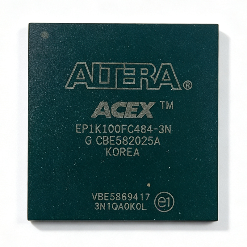
EP1K100FC484-3N - 100K-Gate ACEX 1K FPGA, 484-BGA | Intel
The Intel (formerly Altera) EP1K100FC484-3N is a 100,000-gate ACEX 1K family Field-Programmable Gate Array (FPGA) built on a 2.5V, 0.22 µm CMOS process, packaged in a 484-ball FineLine BGA (FBGA) and offering 333 user I/Os, 4,992 logic elements, 49,152 RAM bits, and a -3 speed grade with internal operating frequencies up to 200 MHz. The device combines a 4-input look-up-table (LUT) logic fabric with embedded array blocks (EABs) that implement RAM, ROM, dual-port RAM, or first-in first-out (FIFO) memory without external components. An FPGA (Field-Programmable Gate Array) is a programmable logic device that lets engineers implement arbitrary digital logic, signal-processing datapaths, glue logic, and embedded memory on a single chip after PCB fabrication. In the broader hierarchy, an FPGA sits above simple PAL/GAL SPLDs, above CPLDs, and below ASICs - it occupies the high-density, high-flexibility tier of programmable logic. The ACEX 1K family was Altera's first low-cost, die-efficient architecture that paired LUT-based logic with embedded memory, targeting system-on-a-programmable-chip (SOPC) designs. Key features include 624 logic array blocks (LABs), 12 EABs providing 49,152 bits of embedded memory, multiVolt I/O support for interfacing with 2.5V, 3.3V, and 5V systems, JTAG-based IEEE 1149.1 boundary-scan test, in-system programmability via the passive serial configuration scheme, and a dedicated configuration circuitry. The 484-ball FBGA package supports 333 user I/O pins - among the highest in the ACEX 1K family - enabling wide parallel buses, multiple communication interfaces, and address/data multiplexing for external memory or bus peripherals. Typical applications span telecommunications line cards, industrial control and factory automation, glue logic and bus bridging, glue-logic replacement of discrete 74-series logic, DSP pre/post-processing, and legacy ASIC prototyping. The combination of 100K ASIC gates of logic, dual-port RAM, and a 200 MHz internal fabric makes the EP1K100FC484-3N a practical choice for cost-sensitive volume production where an ASIC is not yet economical. When designing with the EP1K100FC484-3N, plan the I/O bank voltage assignments early because the device supports 2.5V, 3.3V, and 5V interfaces through multiVolt I/O but requires careful reference-voltage planning. The configuration scheme (PS, JTAG, or PPA) must be selected before PCB layout, and decoupling capacitors must be placed within 100 mils of every VCCINT and VCCIO pin. This page consolidates distributor pricing, same-brand drop-in equivalents, and ACEX 1K design considerations not available on a single manufacturer datasheet page, giving engineers a one-stop reference for sourcing and selecting this legacy FPGA.
EP1K100FC4842N - ACEX-1K 100K Gate FPGA, 484-BBGA | Altera
The Altera (Intel) EP1K100FC4842N is a member of the ACEX-1K programmable logic device family, providing low-cost system-on-a-programmable-chip (SOPC) integration in a single 484-ball BGA package. It features 100,000 typical gates, 49,152 bits of embedded array (EAB) memory, 4,992 logic elements, and 333 user I/O pins. The device operates from a 2.5V core supply with the "-2" speed grade, making it suitable for cost-sensitive high-volume designs. A Field-Programmable Gate Array (FPGA) is a semiconductor device built around a matrix of configurable logic blocks (CLBs), programmable interconnects, and I/O cells that allow the device to be reconfigured post-manufacturing for almost any digital function. FPGAs sit between general-purpose microcontrollers and fixed-function ASICs in the programmable logic hierarchy: gate array -> programmable logic device (PLD) -> complex PLD (CPLD) -> field-programmable gate array (FPGA) -> SoC FPGA. They offer hardware-level parallelism, deterministic timing, and rapid design iteration through HDL-based synthesis. Key features of the EP1K100FC4842N include 12 embedded array blocks (EABs) providing dual-port RAM up to 49152 bits total, tristate buffers per LAB for bus-oriented applications, multi-volt I/O support for 2.5V, 3.3V, and 5.0V mixed-voltage interfaces, JTAG-compliant boundary-scan testing (IEEE 1149.1), and built-in PCI compliance at 66 MHz. The device supports up to 49,152 RAM bits of true dual-port memory with byte enables, parity checking, and shift-register mode. The EP1K100FC4842N uses a SRAM-based Look-Up Table (LUT) architecture with a 0.18 µm CMOS process and 4-input LUTs, achieving density efficiency at low cost. Its continuous routing architecture uses direct-drive, fast-path connections for predictable timing closure. The "-2" speed grade denotes the second-fastest bin in the family, balancing Fmax and price for mainstream logic designs. Typical applications include PCI bus interfaces, bus bridges, DSP datapath acceleration, telecommunications line cards, industrial control, and embedded control blocks in copiers, network switches, and routers. Multi-volt I/O makes the part especially useful as a glue-logic bridge between 5V legacy ASICs and 3.3V processors. When designing with this device, plan for a 2.5V regulated core supply and separate VCCIO rails per I/O bank. The 484-BBGA package requires careful PCB stack-up and BGA escape routing. Use the Altera Quartus development suite for synthesis, place-and-route, and timing analysis. This page synthesizes distributor stock signals, drop-in pin-compatible ACEX-1K variants, and practical design notes not aggregated in the original ACEX-1K datasheet (Altera ACEX-1K Programmable Logic Device Family Data Sheet).
EP1K100FI256-2 - 100K Gate ACEX 1K FPGA, 256-BGA | Intel / Altera
The Intel (formerly Altera) EP1K100FI256-2 is an ACEX 1K family Field Programmable Gate Array (FPGA) delivering 100,000 system gates with 4,992 logic elements in a 256-ball FineLine BGA package. Per the manufacturer datasheet, the device integrates a look-up table (LUT)-based logic fabric with embedded array blocks (EABs) and is fabricated on a 2.5 V CMOS process supporting maximum operating frequencies up to 250 MHz. The "-2" speed grade designates a mid-range performance bin between the -1 (slower) and -3 (faster) ACEX 1K variants. A Field Programmable Gate Array (FPGA) is a type of programmable logic device (PLD) that combines configurable logic blocks, programmable interconnect, and I/O cells on a single die. Within the broader semiconductor taxonomy, FPGAs belong to programmable logic -> logic ICs -> integrated circuits. The ACEX 1K family occupies the low-cost system-on-a-programmable-chip (SOPC) tier of the Altera/Intel portfolio, combining LUT logic with EAB memory for efficient megafunction implementation such as FIFO buffers, RAM blocks, and specialized I/O functions. Key features of the EP1K100FI256-2 include 49,152 bits of embedded memory distributed across EABs, 186 user I/Os supporting multiple I/O standards, 2.5 V core supply with 3.3 V tolerant I/O, and in-system programmability via IEEE 1149.1 JTAG and Altera-specific configuration schemes. The device supports dual-port EAB memory and includes built-in clock management for synchronous design implementation. The architecture combines a die-efficient LUT fabric with EABs that can be configured as dual-port RAM, ROM, or specialized logic functions, providing an optimal balance between logic density and on-chip memory. The 0.22 µm CMOS process delivers predictable timing closure suitable for glue-logic, bus interfacing, and protocol bridging applications in cost-sensitive industrial and communications equipment. Typical applications include industrial control glue logic, communications protocol bridging, peripheral bus interfacing (PCI, ISA, UART bridges), low-density DSP preprocessing, and legacy system modernization. The 256-FBGA package supports compact board layouts while exposing the full 186 user I/O count for high-pin-count bridging scenarios. When designing with this device, verify Quartus or MAX+PLUS II support for the ACEX 1K family, as Intel has formally discontinued new ACEX 1K design entries in modern toolchains. The "FI" package code indicates industrial temperature grade (-40 °C to +85 °C) suitable for harsh-environment deployments. This page synthesizes distributor pricing, drop-in alternatives from the same ACEX 1K family, and practical design notes for legacy FPGA migration not found in the original manufacturer datasheet.
EP1K100FI256-2N - ACEX 1K FPGA 100K Gates 256-BGA | Intel
The Intel (formerly Altera) EP1K100FI256-2N is a member of the ACEX 1K family of Field Programmable Gate Arrays, integrating 100,000 system gates, 4,992 logic elements (LEs), 49,152 RAM bits and 186 user I/O pins into a 256-ball FineLine BGA package rated for industrial temperature operation. The device is fabricated on a 0.22 µm SRAM-process technology node, operates from a 2.5 V core supply, and supports configuration via the IEEE Std. 1149.1 boundary-scan JTAG interface plus serial configuration modes, allowing field upgrades of design bitstreams. A Field Programmable Gate Array (FPGA) is a type of programmable logic device (PLD) that combines the integration density of an application-specific integrated circuit (ASIC) with the flexibility of in-system reprogrammability. The ACEX 1K family in particular implements an embedded-array architecture (EAB-based) intended for low-cost system-on-a-programmable-chip (SOPC) designs, bridging the gap between classic CPLDs and high-density FPGAs and serving as the architectural ancestor of the subsequent Cyclone series. Key features include 624 logic array blocks (LABs), six embedded array blocks (EABs) of 4,096 RAM bits each for dual-port RAM or ROM, dedicated clock and clock-enable signals per LAB, MultiVolt I/O support for interfacing to 2.5 V, 3.3 V and 5.0 V buses, and tri-state buffering on every I/O. The '-2N' speed grade corresponds to the faster of the two commercial-grade timing bins and the 'N' suffix denotes leaded (SnPb) ball finish. Hot-swap-friendly I/O and joint Test Action Group (JTAG) boundary scan simplify board bring-up. Architecturally, each LAB contains 16 LEs with a 4-input look-up table (LUT), a programmable carry chain for fast adders, and a cascade chain for wide fan-in functions; the six EABs provide configurable true-dual-port or simple-dual-port memory blocks usable as RAM, ROM, or content-addressable logic. The Quartus II (or MAX+PLUS II for legacy flows) toolchain synthesises Verilog HDL and VHDL into a bitstream that is loaded into the on-chip SRAM configuration memory at power-up. Typical applications include industrial glue-logic replacement, bridge and protocol-conversion cards, low-volume ASIC prototyping, motor-control and motion-control state machines, telecom line-card glue, and embedded DSP pre/post-processing front-ends. The 256-BGA package is chosen where board real-estate is at a premium and high signal integrity is required. When designing with this FPGA, plan the power-decoupling network with at least one 0.1 µF and one 10 µF low-ESR ceramic capacitor per VCCINT/VCCIO supply pin pair, route all clock signals over a continuous ground reference, and observe the I/O standard signalling level on each bank before mixing 3.3 V and 5.0 V peripherals. Configuration mode and JTAG chain ordering must be validated against the Quartus II programmer before committing to layout. This page synthesises distributor pricing, drop-in compatible alternatives drawn from the ACEX 1K family, and practical design notes not found in the standalone datasheet.
EP1K100FI256-3 - 100K-Gate ACEX 1K FPGA, 186 I/O, FBGA-256 | Intel
The Intel (formerly Altera) EP1K100FI256-3 is a 100,000-gate ACEX 1K family Field-Programmable Gate Array (FPGA) in a 256-ball FineLine BGA package with industrial-grade temperature rating and a -3 speed grade. Per the verified distributor data, the device exposes 6 dedicated inputs and 186 user I/O pins, operates from a 2.5 V nominal core supply (2.375 V to 2.625 V), and is specified over -40 C to +85 C. It implements the classic ACEX 1K architecture of 4,992 logic elements backed by embedded array blocks (EABs), delivering up to 49,152 RAM bits for distributed on-chip memory. What is an FPGA? A Field-Programmable Gate Array is a semiconductor integrated circuit whose logic function is defined after manufacture by a configuration bitstream loaded into on-chip SRAM. FPGAs sit in the broader taxonomy of programmable logic devices (PLDs) > complex PLDs (CPLDs) > FPGAs > SRAM-based LUT FPGAs > ACEX 1K. They are used when designers need high logic density, parallel I/O, and reconfigurability that microcontrollers and ASICs cannot match. The ACEX 1K family was Altera's first SRAM-based family to integrate embedded array blocks for true system-on-chip integration. Key features of the EP1K100FI256-3 include 100,000 typical gates, 4,992 logic elements, 49,152 RAM bits distributed across EABs, 186 user I/O pins, JTAG-compliant IEEE 1149.1 boundary-scan support, and a dedicated configuration interface. The device is built on a 0.22 micron CMOS process and supports in-system programmability through its SRAM configuration cells, allowing unlimited reconfiguration during development and in-field updates. The -3 speed grade places this part in the mid-performance tier of the ACEX 1K family, with the family datasheet quoting Fmax in the 180-200 MHz range depending on the speed grade selected. The FineLine BGA-256 (FBGA-256) package provides a compact footprint while supporting high pin counts for parallel buses and high-density I/O expansion. This combination makes the EP1K100FI256-3 suitable for legacy designs, prototyping, and industrial glue logic where form factor and I/O density matter. Typical applications include industrial control glue logic, communication interface bridging, legacy peripheral expansion, ASIC prototyping emulation, and parallel data acquisition front-ends. The 186 available I/O pins accommodate wide parallel buses and multi-protocol bridging without external muxing. When designing with this part, plan configuration scheme (JTAG, PS, or AS) early because the configuration interface dictates board layout for the EPC or serial configuration device. Because ACEX 1K is a multi-decade mature family, expect long lead times and verify second-source availability before committing to a new design. This page synthesizes distributor pricing, drop-in compatible ACEX 1K variants, and practical sourcing notes not consolidated in a single datasheet, helping engineers and buyers evaluate form-fit-function compatibility for legacy and new designs.
EP1K100FI484-2 - 100K Gate ACEX-1K FPGA 2.5V 484-FBGA | Intel
The Intel (formerly Altera) EP1K100FI484-2 is a member of the ACEX-1K family of Field Programmable Gate Arrays (FPGAs), delivering 100,000 typical gates and 4,992 logic elements (cells) in a 484-ball FineLine BGA (FBGA) package with 333 user I/O pins. The device is built on a 2.5V CMOS process and supports system clock rates up to 250 MHz, integrating embedded array blocks (EABs) for efficient memory and specialized logic functions. It is graded for industrial temperature operation (-40C to +85C) and ships in a surface-mount FBGA-484 package suitable for high-density logic designs. What is an FPGA? An FPGA (Field Programmable Gate Array) is a type of programmable logic device (PLD) that allows engineers to implement custom digital circuits after manufacture. In the broader taxonomy, FPGAs sit at the top of the programmable logic hierarchy: PLD -> CPLD -> FPGA -> SoC FPGA. Each FPGA contains configurable logic blocks (LEs), programmable interconnect, and I/O elements, all controlled by a vendor-specific configuration bitstream. The ACEX-1K family is part of Intel's (Altera's) low-cost, high-volume FPGA line targeting glue logic, bridge, and control-plane applications. The EP1K100FI484-2 features 49,152 memory bits distributed across its EABs, 333 maximum user I/O pins, and supports in-system programming via the IEEE 1149.1 (JTAG) interface and Altera's proprietary configuration schemes. Its embedded array blocks enable implementation of megafunctions such as dual-port RAM, ROM, and specialized arithmetic functions without consuming general-purpose logic, reducing overall die area and improving timing closure for memory-intensive designs. Typical applications include digital signal processing front-ends, telecommunications glue logic, industrial control and instrumentation, video and image processing pipelines, and PCI/CompactPCI bridge interfaces. The 484-pin FBGA package supports high I/O count designs with signal integrity advantages over lower-pin-count packages. When designing with this device, ensure that the Quartus II (or MAX+PLUS II) toolchain supports the targeted speed grade and that PCB layout provides sufficient decoupling and matched impedance for high-speed I/O. The -2 speed grade indicates a mid-tier performance bin; the -1 grade is faster and the -3 grade is the slowest. Engineers should review the ACEX-1K family datasheet for I/O standard support, configuration timing, and power estimation guidance. This page synthesizes distributor availability, drop-in pin-compatible ACEX-1K alternatives, and practical design considerations not found in the manufacturer datasheet alone.
EP1K100FI484-2N - 100K ACEX-1K FPGA 333 I/O | Intel (Altera)
The Intel (formerly Altera) EP1K100FI484-2N is a high-density ACEX-1K family Field Programmable Gate Array (FPGA) integrating 100,000 typical gates, 49,152 RAM bits, and 333 user I/Os into a 484-ball FineLine BGA package (23 mm x 23 mm). It is built on a 2.5 V SRAM-based look-up table architecture with embedded array blocks (EABs) for memory and specialized logic functions, and is supported by the Quartus II design software toolchain. The "-2N" speed grade and industrial temperature rating (-40C to +85C) make it suitable for cost-sensitive, performance-oriented designs. An FPGA (Field Programmable Gate Array) is a semiconductor device containing an array of configurable logic blocks (CLBs), programmable interconnects, and I/O cells that can be reconfigured by the designer after manufacture. Within the broader taxonomy, FPGAs belong to programmable logic devices (PLDs), alongside CPLDs and PALs, and are categorized under digital logic ICs. The ACEX-1K family sits between simple PLDs and high-density SRAM-based FPGAs, offering low-cost system-on-a-programmable-chip (SOPC) integration in a single device for glue-logic and bus-interface applications. Key features of the EP1K100FI484-2N include 624 logic array blocks (LABs), 4,992 logic elements, 12 embedded array blocks for memory/FIFO implementations, and the FastTrack continuous routing interconnect for fast, predictable interconnect delays. It supports multiple I/O voltage standards including 3.3 V, 2.5 V, 1.8 V, and 1.5 V LVTTL/LVCMOS, and provides a dedicated carry chain for fast adders, counters, and comparators. Configuration is via passive serial, active serial, or JTAG modes. Typical applications include industrial control and automation glue logic, telecommunications interface bridging, low-cost PCI bus controllers, video processing pipelines, and legacy system upgrades. With 49 Kbits of embedded memory and 333 user I/Os, the device can implement multiple megafunctions in parallel without external memory. Designers should follow Intel's configuration and decoupling guidelines from the ACEX 1K Device Family datasheet to ensure reliable operation across the industrial temperature range. When designing with this part, account for the 2.5 V core VCCINT requirement and provide a stable PLL analog supply. Use multiple decoupling capacitors (0.1 uF and 10 uF) close to each supply pin to minimize switching noise on the 333 I/O channels. This page synthesizes distributor pricing, FPGA-family drop-in alternatives, and practical design notes not found in the original ACEX-1K datasheet, providing engineers with a single decision-ready reference for legacy ACEX-1K designs.
EP1K100FI4842 - 100K Gate ACEX-1K FPGA 484-BGA | Intel / Altera
The Intel / Altera EP1K100FI4842 is a member of the ACEX 1K family of Field Programmable Gate Arrays (FPGAs), delivering 100,000 system gates, 4,992 logic elements, and 49,152 RAM bits in a 484-ball FineLine BGA package. The device integrates 333 user I/O pins, 6 embedded array blocks (EABs) configurable as memory or logic, and operates from a 2.5V core supply with up to 250 MHz internal performance. An FPGA (Field Programmable Gate Array) is a type of programmable logic device (PLD) that allows engineers to implement custom digital logic by configuring an array of configurable logic blocks (CLBs), programmable interconnect, and I/O cells after manufacturing. FPGAs sit at the top of the programmable logic hierarchy: PLD -> CPLD/FPGA -> SRAM-based FPGA -> ASIC prototype, offering higher density and performance than CPLDs while retaining in-system reprogrammability. Key features of the EP1K100FI4842 include 624 LABs (Logic Array Blocks) carrying 8 logic elements each, dual-purpose embedded system blocks (ESBs) usable as RAM, ROM, or product-term logic, JTAG-compliant IEEE 1149.1 boundary-scan support, and MultiVolt I/O supporting 2.5V, 3.3V, and 5.0V interfacing. The 484-FBGA package provides high pin density while still enabling conventional PCB assembly and rework. The EP1K100FI4842 is fabricated on a 0.18 micrometer CMOS SRAM process and is configured at power-on from a serial configuration EPROM such as the EPC2 or EPC8, supporting 4-pin passive serial or byte-wide parallel configuration schemes. The device is targeted at cost-sensitive digital logic integration in telecom line cards, industrial control, and glue-logic consolidation designs. Typical applications include digital signal processing front-ends, telecommunications interface bridging (TDM, HDLC, ATM), industrial protocol bridges, and PCI bridge/logic consolidation. When designing with this device, ensure the configuration EPROM is sized appropriately for the bitstream (approximately 1 Mbit for an ACEX-1K 100K device) and that JTAG chain integrity is verified before in-system programming.

EP1K100QC208-1 - 100K Gate ACEX-1K FPGA, 2.5V, PQFP-208 | Altera
The Altera (now Intel) EP1K100QC208-1 is a 100,000-gate ACEX-1K family Field Programmable Gate Array (FPGA) built on a 2.5V, 0.22 µm SRAM-lookup-table (LUT) process, supplied in a 208-pin Power Quad Flat Pack (PQFP / BFQFP) package with 147 user I/O pins. The device integrates 49,152 bits of embedded dual-port RAM, 4,992 logic elements (LEs), and a 333.33 MHz internal performance figure, providing a low-cost system-on-a-programmable-chip (SOPC) integration point for glue logic, custom state machines, and modest-width bus bridging. An FPGA is a programmable logic device that lets engineers implement arbitrary digital logic, memory blocks, and DSP functions in silicon that can be reconfigured in-circuit. Within the broader programmable logic hierarchy, FPGAs sit above simple PLDs and CPLDs because they contain thousands of LUT-based logic cells, distributed and block RAM, and dedicated routing — they are an instance of programmable logic in the larger semiconductor taxonomy of logic ICs. The ACEX-1K family introduced a fine-grained embedded array structure that combines distributed logic and dedicated memory, allowing per-LE dual-port RAM blocks for FIFO and small cache designs. Key features of the EP1K100QC208-1 include 4,992 logic elements organized into 624 Logic Array Blocks (LABs), 49,152 bits of embedded dual-port RAM with independent read/write ports per block, 147 maximum user I/O pins supporting LVTTL/LVCMOS and other common single-ended I/O standards of the era, in-system programmability via an external serial configuration device or JTAG, and operation from a 2.5V core supply with multi-voltage I/O banks. The part is offered in the commercial temperature grade (the "C" suffix) and at the -1 speed grade. Architecturally, the device pairs a lookup-table-based logic fabric with rows of embedded array blocks (EABs) used for memory and DSP megafunctions. Configuration data is loaded from an external serial or parallel PROM at power-up via the Altera Passive Serial (PS) or Passive Parallel Synchronous (PPS) scheme, supported by the MAX+PLUS II and Quartus design suites on Windows and Unix workstations. The 0.22 µm process and 2.5V core keep dynamic power modest compared to later 90 nm and 65 nm families. Typical applications include industrial control and instrumentation, telecom interface cards, legacy peripheral bridging, glue-logic consolidation, low-volume custom ASIC replacement, and educational platforms teaching HDL synthesis with a proven, well-documented toolchain. Engineers often choose this part when migrating off EOL PLDs or older discrete logic. When designing with this device, pay attention to the 2.5V core supply requirement, the need for a separate configuration PROM on legacy boards, and the 5V-tolerant I/O features that are no longer reproduced on newer Altera/Intel families. Because the ACEX-1K family is mature, plan second-source or migration paths using the SameFrame pin-compatible ACEX-1K options during board bring-up. This page synthesizes distributor pricing, drop-in same-package alternatives, and practical design notes — information not gathered in any single manufacturer document.

EP1K100QC208-1GZ - ACEX-1K FPGA 100K Gates 208-PQFP | Intel
The Intel EP1K100QC208-1GZ is a member of the ACEX-1K family of FPGAs that integrates 100,000 typical gates and 4,992 logic elements (LEs) into a 208-pin Plastic Quad Flat Pack (PQFP/BFQFP) measuring 28x28 mm. Operating from a 2.5 V core supply (2.375 V to 2.625 V), the device delivers up to 250 MHz system performance and exposes 147 user I/O pins, with embedded array blocks (EABs) providing 49,152 bits of dual-port RAM for efficient on-chip memory implementation. An FPGA (Field Programmable Gate Array) is a semiconductor device built around an array of configurable logic blocks (CLBs), programmable interconnect, and I/O cells, allowing designers to implement arbitrary digital logic after PCB assembly. FPGAs sit hierarchically above fixed-function ASICs and below microcontrollers in design flexibility, and are favored for prototyping, low-volume production, and DSP/data-path acceleration. The ACEX-1K family specifically introduced the embedded array block, allowing megafunctions such as efficient memory and specialized logic functions to be implemented alongside general-purpose LEs. Key features of the EP1K100QC208-1GZ include the SameFrame pin migration option with 256-pin FineLine BGA variants, IEEE 1149.1 (JTAG) boundary-scan support, in-system programmability via the MAX+PLUS II or Quartus development systems, and a robust SRAM-based configuration cell that supports fast reconfiguration. The quad flat pack package offers a JEDEC-standard 3.49 mm height profile and a 0.5 mm lead pitch suitable for production through-hole-style surface-mount assembly lines and breadboard-friendly socket adapters during prototyping. The device architecture employs a Look-Up Table (LUT)-based LE fabric with EABs of 4,096 bits each, providing deterministic logic delays and predictable timing closure. The 2.5 V core is paired with multi-standard I/O that supports LVTTL, LVCMOS, SSTL, and PCI signaling through dedicated I/O banks, and the silicon is offered in both commercial and industrial temperature grades with device speed grades of -1 (fastest), -2, and -3. The 'GZ' suffix in the part number denotes a lead-free, RoHS-compliant package. Typical applications include glue logic replacement, bridge and protocol conversion in legacy systems, low-volume telecom line cards, industrial control and instrumentation front-ends, and educational platforms. Its 49,152 bits of embedded RAM and 147 user I/Os are well matched to small DSP filter chains, UART/SPI expansion, and custom state-machine controllers. When designing with this device, ensure that the MAX+PLUS II or Quartus toolchain version supports the ACEX-1K family and that a configuration EPROM (EPC) or JTAG programmer is available. Since the EP1K100 is a mature EOL device, verify long-term availability before new design starts. This page synthesizes distributor pricing, drop-in same-package alternatives from web data, and practical design notes not found in the manufacturer datasheet, giving the engineer a single source for evaluation, comparison, and replacement decisions.
EP1K100QC208-1N - ACEX 1K FPGA 4992 Cells | Altera
The Altera EP1K100QC208-1N is an ACEX-1K family Field Programmable Gate Array (FPGA) fabricated in 0.22 um CMOS technology, providing 100,000 typical gates, 4,992 logic elements, 624 LABs, 49,152 RAM bits and 147 user I/O pins in a 208-pin PQFP package. Verified distributor parametric data lists a 2.5 V core supply and a 333.33 MHz maximum frequency figure for this -1 speed grade. A Field Programmable Gate Array is an integrated circuit whose logic fabric can be configured after manufacturing using HDL design flows. FPGAs sit between fixed-function ASICs and general-purpose processors in the digital component hierarchy: FPGA -> programmable logic device -> integrated circuit -> semiconductor. The ACEX 1K family was Altera's low-cost programmable logic platform, combining an embedded array for memory and specialized functions with configurable logic blocks for user logic. Key EP1K100QC208-1N specifications include 4,992 logic elements, 624 LABs, 147 I/Os, 49,152 RAM bits, a 100K-gate equivalent density, 2.5 V core supply, CMOS 0.22 um process technology, and the 208-pin PQFP/BFQFP package. The N suffix indicates the lead-free variant intended for RoHS-conscious legacy assembly flows. The architecture uses look-up-table-based logic elements and embedded array blocks for memory-intensive functions. With 147 I/O pins, this FPGA can support wide parallel buses, memory interfaces and multiple serial peripherals. The 333.33 MHz parametric maximum makes it suitable for timing-sensitive synchronous systems, although designers should always validate performance with the ACEX 1K timing model. Typical applications include sustaining legacy industrial controllers, telecom protocol bridging, ASIC prototyping, university FPGA teaching labs and service replacement for medical or instrumentation backplanes produced in the early 2000s. The -1N speed grade provides maximum timing margin among the common -1, -2 and -3 ACEX speed bins. When designing with this device, plan for a separate 2.5 V core supply and verify all I/O bank voltage levels. Intel/Altera community guidance indicates that modern FPGAs are not pin-compatible replacements, so legacy boards often require an adapter board or full redesign if moving to a newer family. This page synthesizes distributor availability, same-package ACEX alternatives, pricing estimates, and practical migration notes beyond what is printed in the manufacturer datasheet.
EP1K100QC208-2 - 100K Gate ACEX-1K FPGA, 208-PQFP | Altera
The Altera (Intel) EP1K100QC208-2 is a member of the ACEX-1K family of Field Programmable Gate Arrays (FPGAs), delivering 100,000 equivalent gates and 4,992 logic elements in a 208-pin Plastic Quad Flat Pack (PQFP) package. Built on a 2.5 V CMOS process with a maximum internal clock frequency of 250 MHz, this device integrates 49,152 bits of embedded array memory organized for dual-port operation, alongside 147 user I/O pins that support a broad range of single-ended I/O standards. An FPGA (Field Programmable Gate Array) is a reprogrammable semiconductor device whose logic function is defined by a configuration bitstream loaded into on-chip SRAM. FPGAs sit at the top of the programmable-logic hierarchy, above CPLDs (Complex Programmable Logic Devices) and SPLDs (Simple Programmable Logic Devices). The ACEX-1K family is positioned between low-density CPLDs and high-density FPGAs such as Stratix and Cyclone, making it suitable for mid-range glue logic, bus bridging, and DSP pre-processing tasks. The EP1K100QC208-2 features 624 Logic Array Blocks (LABs), each containing 8 Logic Elements (LEs), giving the device a total of 4,992 LEs for combinational and sequential logic implementation. The embedded array provides efficient memory blocks for FIFO, dual-port RAM, and ROM functions without consuming external logic resources. The 147 user I/O pins are distributed across four I/O banks, each supporting 2.5 V LVTTL/LVCMOS signalling by default and configurable through the Quartus design tool. Typical applications include telecommunications line-card interfaces, industrial control and instrumentation, low-cost glue logic replacement, legacy system prototyping, and education. The PQFP-208 footprint and the mature 2.5 V core also make the part suitable for designs where drop-in compatibility with existing ACEX-1K boards is required. When designing with this device, engineers should note the PQFP-208 package requires careful PCB layout with respect to lead inductance and signal integrity, especially for clock and high-speed I/O nets. The 2.5 V core supply must be tightly regulated, and unused I/O pins should be configured as tri-stated inputs with weak pull-ups to reduce quiescent current. This page synthesises distributor pricing, drop-in ACEX-1K alternatives in the same PQFP-208 footprint, and practical design notes that are not aggregated on a single manufacturer datasheet page.
EP1K100QC208-2N - ACEX-1K FPGA 4992 LE, 147 IO | Altera
The Intel (Altera) EP1K100QC208-2N is an ACEX 1K family field-programmable gate array with 4,992 logic elements arranged in 624 LABs, 49,152 total RAM bits, and 147 user I/O pins, supplied in a 208-pin PQFP package. It operates from a 2.5V core supply, uses CMOS technology, and supports a 0C to 70C commercial temperature range. The -2 speed grade places it between the faster -1 and slower -3 variants in the same 208-pin footprint.\n\nAn FPGA is an integrated circuit whose logic fabric is configured after manufacturing to implement custom digital hardware. Unlike a fixed-function ASIC or microcontroller, an FPGA consists of programmable lookup tables, flip-flops, routing resources, and embedded memory blocks that together form arbitrary logic circuits. In the power-management and processing hierarchy, this product belongs to programmable logic devices, above simple CPLDs in complexity and below application-specific standard parts in unit-volume cost optimization. For designers needing deterministic, parallel digital logic without wafer fabrication, an FPGA provides a fast path between algorithm and hardware.\n\nKey features of the EP1K100QC208-2N include 4,992 logic elements per the verified family specification, 49,152 RAM bits for on-chip packet buffering and FIFO storage, 624 LABs for distributed control logic, and 147 user I/O pins in a 208-pin PQFP. The device uses a 2.5V core voltage, reducing dynamic power compared with 5V predecessors, while the -2 speed grade supports typical clock rates up to about 250 MHz as reported by listings for this part. Altera's ACEX 1K architecture includes an embedded array suitable for implementing memory and specialized logic functions.\n\nThe internal architecture combines logic array blocks with embedded array blocks for system-on-a-programmable-chip integration. This allows functions such as dual-port RAM, CAM, and DSP storage to reside on-chip, reducing board area and latency. The technology is CMOS 0.22um, and the part is classified as obsolete at end-of-life status in current distributor records. Because ACEX 1K uses SRAM-based configuration, an external boot source such as an EPC configuration device is required to load the bitstream after power-up.\n\nTypical applications include protocol bridging, industrial I/O control, image preprocessing, data acquisition in test instrumentation, and legacy product lifecycle replacement. The 147 I/O count is sufficient for 32/64-bit data paths plus handshaking, and the 49,152 RAM bits support small FIFOs and line buffers. For designs that need parallel throughput rather than sequential processing, the EP1K100QC208-2N can implement several bus converters or custom state machines in a single device.\n\nWhen designing with this component, remember that it is volatile and obsolete. Add an EPC2 or host-processor configuration path, maintain the 2.5V core rail with adequate bulk capacitance, and confirm current stock before committing to a large production run because no modern pin-compatible FPGA replacement exists. For new designs, select a current FPGA family instead of ACEX 1K.\n\nThis page synthesizes distributor pricing, drop-in speed-grade alternatives, architecture notes, and practical configuration guidance not repeated in raw datasheet snippets, giving engineers a compact cross-reference for maintaining legacy ACEX 1K systems.
EP1K100QC208-2NGZ - ACEX-1K 100K Gates FPGA, 147 I/O, 208-PQFP | Intel / Altera
The Intel / Altera EP1K100QC208-2NGZ is a member of the legacy ACEX-1K family of Field Programmable Gate Arrays (FPGAs), delivering 100,000 typical gates and 4,992 logic elements in a 208-pin Plastic Quad Flat Pack (208-BFQFP / 208-PQFP) surface-mount package. The device integrates 624 Logic Array Blocks (LABs) / Configurable Logic Blocks (CLBs), 49,152 bits of embedded SRAM, 147 user I/O pins, and operates from a 2.375V to 2.625V core supply with a commercial 0°C to 70°C temperature grade. What is an FPGA? A Field Programmable Gate Array is a semiconductor integrated circuit built around an array of configurable logic blocks (CLBs/LABs) connected by a programmable interconnect matrix. Unlike an ASIC (Application-Specific Integrated Circuit), an FPGA can be reconfigured in the field after manufacturing, making it ideal for prototyping, low-volume production, glue logic, and applications where design changes are expected. Within the FPGA taxonomy, the EP1K100 sits at the lower-density end: CPLD -> low-density FPGA -> ACEX-1K -> high-density FPGA -> SoC FPGA. Key specifications include a 2.5V core supply with 5V-tolerant I/O, in-system programmability via the Altera ByteBlaster or BitBlaster configuration interface, and JTAG boundary-scan support. The 'QC208' package code denotes the 208-pin Plastic QFP, the '-2' speed grade indicates the medium-speed tier, and the 'NGZ' suffix indicates the lead-free, RoHS-compliant commercial processing variant. The EP1K100QC208-2NGZ uses a SRAM-based Look-Up Table (LUT) architecture with four-input LUTs per logic element, and a hierarchical interconnect structure with FastTrack routing. The embedded array blocks (EABs) provide dedicated dual-port RAM resources that are widely used for FIFO buffers and small register files. Configuration data is loaded from an external serial or parallel PROM at power-up, since the SRAM cells are volatile. Typical applications include digital signal processing front-ends, industrial control glue logic, telecommunications line-card interfaces, PCI bridge controllers, and legacy embedded systems where the ACEX-1K has been a long-standing design-in. The 147 user I/Os are sufficient to drive multiple 16/32-bit buses and external memory interfaces in cost-sensitive designs. When designing with this device, ensure that configuration memory (typically an EPC2 or EPC16) is included in the BOM, since the EP1K100 has no on-chip non-volatile configuration storage. Decoupling must follow the ACEX-1K Hardware Reference Manual guidelines: 0.1µF + 10µF near each VCCINT pin group. Note that ACEX-1K is now in legacy/discontinued status, so designers should evaluate Cyclone or Cyclone II for new designs. This page synthesizes distributor stock levels, drop-in same-package ACEX-1K alternatives, and practical design notes not found in the original manufacturer datasheet.
EP1K100QC208-3 ACEX 1K FPGA 100K Gates | Altera
The Altera EP1K100QC208-3 is an ACEX 1K field-programmable gate array (FPGA) fabricated in 0.22 um CMOS with 4,992 logic elements, 49,152 bits of on-chip RAM, and 147 user I/O pins, housed in a 208-lead BFQFP/PQFP package. It is supplied for a 2.5 V core operating environment and is characterized for 200 MHz internal clock operation at the -3 speed grade. An FPGA is a semiconductor device containing programmable logic blocks and programmable interconnects that can implement arbitrary digital logic after manufacturing. In the ACEX 1K architecture, the configurable fabric is organized into logic array blocks (LABs), each containing smaller logic elements, plus embedded array blocks for memory. EP1K100QC208-3 sits in the hierarchy FPGA > programmable logic device > integrated circuit, and is specifically a 2.5 V SRAM-based programmable logic family used when a designer needs field reconfigurability without committing to a fixed ASIC. Key features are the 100K typical gate capacity, 624 LABs, 4,992 logic elements, 49,152 RAM bits, and 147 user I/O pins. The 208-terminal square BFQFP has gull-wing leads and is intended for conventional surface-mount assembly. The device is rated for the commercial temperature grade and uses a 0.22 um CMOS process. These parameters make it suitable for moderate-density logic integration and interface consolidation on boards that already use 2.5 V logic. The EP1K100QC208-3 is a loadable PLD, meaning it is configured from external memory or a programming host each time it powers up. Its internal architecture is designed for register-rich control logic, state machines, bus bridging, and small FIFO memories rather than high-speed DSP or embedded processor tasks. The 200 MHz internal speed indicates the practical performance ceiling of the -3 speed grade, while the 147 I/O pins are individually programmable and can be assigned to different board-level functions under the fitter. Typical applications include replacement logic in legacy telecommunications line cards, industrial automation I/O controllers, medical data acquisition systems, test and measurement trigger generation, and ASIC prototyping where a fixed gate-array design has not yet been completed. The 100K gate density and 49,152 RAM bits are well matched to block-level control logic and medium-width protocol state machines. One design consideration is that the device is SRAM-based; the configuration bitstream must be reloaded at every power-up, normally from an Altera EPC configuration device or through a download cable. The PCB must therefore include configuration-data connections, not just the FPGA core supply and user I/O net. This page provides distributor-level stock and pricing context, same-family drop-in replacement guidance, and practical board-level notes that are not repeated in the original manufacturer datasheet, helping engineers determine whether EP1K100QC208-3 fits an existing legacy BOM.
EP1K100QC208-3N - ACEX-1K FPGA 100K Gates | Altera
The Altera EP1K100QC208-3N is a 100K-gate ACEX-1K field-programmable gate array (FPGA) containing 4,992 logic elements, 624 LABs, 49,152 embedded RAM bits, and 147 user I/Os, supplied in a 208-pin BFQFP (plastic quad flat pack) package with a 2.5V core and a 200MHz internal clock rating. An FPGA is a semiconductor device whose logic fabric and routing can be reprogrammed in-system to implement arbitrary digital functions. ACEX-1K sits between simple CPLDs and dense high-end FPGAs: it provides SRAM-based look-up table logic with embedded array blocks (EABs) for on-chip memory, making it useful for protocol bridging, video timing, and custom peripheral controllers. In the device hierarchy it belongs to programmable logic devices (PLDs), specifically SRAM-based FPGAs, and the package family is plastic quad flat pack (PQFP/BFQFP) in a surface-mount form. Key features include 4,992 logic elements arranged in 624 logic array blocks, 49,152 RAM bits usable as FIFOs or dual-port RAM, 147 user I/O pins that can connect to 2.5V/3.3V logic systems, built-in JTAG boundary-scan test circuitry compliant with IEEE Std. 1149.1-1990, and the -3 speed grade rated for a 200MHz internal clock. The device uses a 2.5V CMOS core with a low-power SRAM-based configuration cell. The ACEX-1K architecture combines look-up-table logic with dedicated carry chains for arithmetic and embedded array blocks for efficient memory. This structure allows compact implementations of counters, state machines, small processors, and bus interfaces. The 208-pin BFQFP provides 147 accessible I/O pins, with the remaining pins allocated to power, ground, configuration, and JTAG functions. Its square gull-wing package can be assembled on standard PCB processes without a BGA socket or interposer. Typical applications include communications line cards, industrial control bridging, scan-rate conversion, display timing controllers, and glue-logic replacement in legacy digital systems. Because the 100K typical gate count and 49,152 bits of RAM are large for its era but moderate today, engineers often use the EP1K100QC208-3N to prototype digital logic before migrating to a current FPGA, or to patch an existing ACEX-1K board without changing the PCB. One important design consideration is decoupling and I/O voltage. Core and I/O supplies should be filtered with 0.1uF ceramic capacitors, and the 2.5V core must reach all power pins with a low-impedance plane. If configuration data is stored in an external EPROM, the EPC2/EPC16 configuration device must be selected for ACEX-1K compatibility. This page synthesizes distributor pricing, drop-in alternatives, and practical design notes not found in the manufacturer datasheet. It enables engineers to compare EP1K100QC208-3N with higher speed grades, verify package compatibility, and plan a trustworthy upgrade path for existing ACEX-1K hardware.
EP1K100QI208-02 - 100K Gate ACEX-1K FPGA, 208-PQFP | Altera
The Altera EP1K100QI208-02 is a member of the ACEX-1K family of Field Programmable Gate Arrays (FPGAs) delivering 100,000 system gates, 4,992 logic elements, and 49,152 RAM bits in a 208-pin Plastic Quad Flat Pack (PQFP/BFQFP) package. Built on a 0.22 µm SRAM process and operating from a 2.5 V core supply, it supports up to 147 user I/O pins and a maximum toggle frequency of 250 MHz. The "-02" speed grade is the slowest commercial bin in this family and is appropriate for cost-sensitive, non-timing-critical designs. An FPGA (Field Programmable Gate Array) is a type of programmable logic device (PLD) that combines an array of configurable logic blocks (LABs), embedded memory, and programmable interconnect into a single semiconductor IC. FPGAs belong to the broader hierarchy: programmable logic device -> field programmable gate array -> SRAM-based FPGA -> ACEX-1K family. Unlike ASICs, FPGAs are reprogrammable in-system, which makes them ideal for prototyping, low-volume production, and designs where hardware requirements evolve over time. The EP1K100QI208-02 provides 624 Logic Array Blocks (LABs), each containing 8 Logic Elements (LEs) for a total of 4,992 LEs. Embedded array blocks (EABs) deliver up to 24 Kbits of dual-port RAM per EAB, configurable as RAM, ROM, or FIFO. The device supports in-system configuration via serial or parallel configuration devices, JTAG boundary-scan testing (IEEE 1149.1), and MultiVolt I/O supporting 2.5 V, 3.3 V, and 5 V interfacing, eliminating the need for external level translators in mixed-voltage systems. Architecturally, the ACEX-1K family was the industry's first FPGA to embed dedicated dual-port RAM blocks (EABs), enabling efficient memory-intensive functions such as FIFOs, look-up tables, and DSP-style filtering without consuming logic resources. The 0.22 µm process combined with 2.5 V core reduced power consumption relative to 5 V FPGAs of the era, while the high I/O count (147 user I/Os) makes the device suitable for bus-intensive glue logic, peripheral bridging, and legacy industrial control applications. Typical applications include telecommunications line-card interface glue logic, industrial machine control and instrumentation, ASIC prototyping, peripheral bus bridges (PCI-to-ISA, UART muxing), low-cost digital signal processing front-ends, and embedded control logic. The 208-pin PQFP package is through-hole-friendly and easy to hand-prototype, though it occupies significant PCB area compared to later BGA packages. The wide MultiVolt I/O range also makes the part common in mixed 3.3 V/5 V systems. When designing with the EP1K100QI208-02, note that the "-02" speed grade has the slowest timing margins - it is suitable for designs clocked at 100 MHz or below, but applications requiring 200 MHz+ should select the "-1" speed grade. ACEX-1K devices are now in their end-of-life (EOL) era; for new designs, current Altera/Intel families such as Cyclone IV, MAX 10, or Cyclone V are recommended replacements. This page synthesizes distributor stock and pricing data, ACEX-1K family drop-in alternatives, and practical design notes that are not consolidated in the manufacturer datasheet alone.