Amplifier ICs
بەرهەمەکان (3,200+)

OPA345UA - 3MHz RRIO Op Amp | Texas Instruments
Texas Instruments OPA345UA is a single-amplifier, rail-to-rail input and output operational amplifier designed for low-power, precision signal-conditioning applications. Its headline specifications are a 5.5 V maximum supply, 3 MHz gain-bandwidth product, and an 8-pin SOIC package. The device operates from a single 2.5 V to 5.5 V supply, while its input common-mode range extends approximately 300 mV beyond the supply rails. An operational amplifier, commonly abbreviated op amp, is an analog active component that amplifies the voltage difference between two inputs. The OPA345 belongs to the rail-to-rail input and output, or RRIO, family, allowing its input and output voltages to approach the positive and negative supply limits. Within the broader hierarchy, it is an analog integrated circuit, an operational amplifier, and ultimately a semiconductor used for signal conditioning, sensing, buffering, and closed-loop control. The 3 MHz gain-bandwidth product supports signal amplification where bandwidth is important but low power and small package size remain primary constraints. Its single-amplifier configuration makes it suitable for circuits needing one independently controlled amplifier rather than a multi-amplifier package. Rail-to-rail input capability improves usable signal range in low-voltage systems, particularly when sensor outputs can move close to the supply rails. The manufacturer describes the OPA345 as a low-power CMOS operational amplifier for precision, miniature applications. OPA345UA operates from 2.5 V to 5.5 V and includes approximately 300 mV of input headroom beyond the supply rails. The 300 mV extension helps preserve common-mode operation when a driven signal approaches a rail, although designers must still verify the complete operating range under temperature, load, and output-voltage conditions. The 8-pin SOIC package provides a conventional surface-mount footprint compatible with standard assembly and inspection processes. Typical uses include low-voltage sensor conditioning, portable instrumentation, audio signal paths, data acquisition, and general-purpose analog filtering. In an instrumentation design, the amplifier can buffer a high-impedance sensor before conversion by an ADC. In a portable instrument, the single-supply architecture simplifies rail planning. Designers should nevertheless confirm offset voltage, input bias current, noise density, slew rate, output-current capability, and stability requirements against the manufacturer datasheet before releasing a production design. A key design consideration is the distinction between maximum specification and a usable design margin. The 5.5 V supply limit should not be treated as a target operating point, and signals should not be expected to reach the physical supply rails under every load. Decoupling, grounding, feedback-component selection, output loading, and the chosen noise-gain network all affect achievable accuracy and stability. This product page combines the exact orderable-part details, package information, application context, design guidance, and replacement constraints for OPA345UA. It also identifies which operating characteristics still require confirmation from the manufacturer datasheet, helping engineers move from general amplifier selection to a board-level design more efficiently.

OPA347PA - 350kHz Micropower RRIO Op Amp | Texas Instruments
The Texas Instruments OPA347PA is a single, 5.5 V, 350 kHz micropower operational amplifier with 20 uA quiescent current and rail-to-rail input and output operation, housed in an 8-pin PDIP package. Its combination of low supply current, extended input range, and moderate gain-bandwidth product makes it suitable for portable, battery-powered, and low-power signal-conditioning systems. An operational amplifier is an analog integrated circuit that amplifies the voltage difference between its inverting and non-inverting inputs while using negative feedback to set a stable closed-loop gain. The OPA347 belongs to the hierarchy of operational amplifier, voltage-feedback amplifier, analog amplifier, and semiconductor. Rail-to-rail input and output, commonly abbreviated RRIO, allow the amplifier to operate near the supply rails without requiring a reduced common-mode or output-voltage range. The principal features of the OPA347 are its 5.5 V maximum supply voltage, 350 kHz gain-bandwidth product, and low quiescent current. According to the manufacturer datasheet, the input range extends 200 mV beyond the supply rails, while the output range reaches within 5 mV of the rails. These characteristics support sensor interfaces, low-current signal conditioning, portable instrumentation, and analog measurement circuits. The OPA347 uses a low-power amplifier architecture optimized for speed-to-power performance rather than the bandwidth of a high-speed operational amplifier. Its 350 kHz bandwidth is adequate for low-frequency sensor signals and general-purpose analog conditioning. Input operation beyond the nominal rails improves usable signal range in low-voltage systems, although common-mode, output-swing, and supply-voltage limits must still be respected during design. Typical uses include battery-powered sensor conditioning, portable biomedical instrumentation, low-power data acquisition, current sensing, and buffering. It is particularly appropriate where the signal bandwidth is well below 350 kHz and the 20 uA nominal quiescent current is valuable for extending battery life. The device can also serve as a general-purpose amplifier or voltage follower when low-noise settling and low standby consumption are priorities. Designers should verify the complete common-mode and output-swing curves at the intended supply voltage and load current. Decoupling capacitors should be placed close to the supply pins, input bias currents should remain below the source impedance, and the feedback network should be evaluated for output-capacitance stability. The PDIP package is suited to prototypes, educational assemblies, and through-hole production runs where a surface-mount package is unnecessary. This page organizes the OPA347PA specifications, package details, practical design guidance, verified-source references, and same-family replacement information into one engineering-focused reference. It also identifies which operating parameters require confirmation in the manufacturer datasheet rather than presenting unsupported values as fixed design limits.
OPA347UA - 5.5V 350kHz RRIO Op Amp | Texas Instruments
The Texas Instruments OPA347UA is a single, rail-to-rail input and output operational amplifier with a 5.5 V maximum supply voltage, 350 kHz gain-bandwidth product, and 20 uA low quiescent current in an 8-pin SOIC package. It is designed for low-voltage, low-power signal-conditioning systems where compactness, rail-to-rail operation, and modest bandwidth are more important than high-speed performance. An operational amplifier is an analog integrated circuit that amplifies the voltage difference between its inverting and non-inverting inputs while using negative feedback to set the closed-loop gain. The OPA347 belongs to the operational-amplifier hierarchy within analog signal-chain ICs. Its rail-to-rail input and output capability allows the signal and output ranges to approach the supply rails, which is useful in systems powered from a single low-voltage source. The OPA347UA's headline characteristics are its 5.5 V supply limit, 350 kHz gain-bandwidth product, and 20 uA quiescent current. The low quiescent current reduces the supply demand of continuously powered circuits, while the 350 kHz bandwidth supports low-frequency filtering, buffering, and gain stages. Its single-amplifier configuration reduces board area compared with a dual or quad device when only one signal path is required. Texas Instruments describes the OPA347 family as a microPower, low-cost operational-amplifier family offered in several packages. The OPA347UA is the single-amplifier 8-pin SOIC option. Because its bandwidth is modest, the device is most appropriate for slow sensor, instrumentation, and control signals rather than high-speed data acquisition, video, or RF signal chains. Typical uses include low-power sensor conditioning, buffered transducer interfaces, active filters, battery-powered monitoring, and general-purpose gain stages. The rail-to-rail behavior is especially useful when the signal source can operate near ground or near the positive supply rail. Designers must still confirm common-mode limits, output swing, stability, and noise performance against the exact operating conditions in the manufacturer datasheet. For PCB design, use short feedback paths, maintain a clean ground reference, and place the bypass capacitor close to the supply pins. Do not assume that every rail-to-rail input stage produces the same distortion, offset, noise, or common-mode behavior. Compare the complete electrical characteristics across temperature when precision is required. This product page consolidates the verified OPA347UA operating characteristics, package information, sourcing path, design considerations, and application guidance. It also distinguishes confirmed drop-in alternatives from related family members and explicitly identifies parameters that require confirmation against the Texas Instruments datasheet before design release.
OPA349UA - 1uA, 70kHz Low-Power RRIO Op Amp | TI
Texas Instruments OPA349UA is a single-circuit, rail-to-rail input and output CMOS operational amplifier featuring 70 kHz gain-bandwidth product, 1 µA quiescent current, and operation up to a 5.5 V supply in an 8-pin SOIC package. It is optimized for portable instrumentation and other low-power analog systems. A rail-to-rail input/output operational amplifier, commonly called an RRIO op amp, amplifies the voltage difference between its two inputs while accepting input signals near or beyond the supply rails and producing output voltage close to the rails. This input/output flexibility makes the OPA349 useful in battery-powered sensors, portable instruments, and low-voltage measurement systems where signal headroom is limited. The OPA349UA combines a 70 kHz gain-bandwidth product with only 1 µA of quiescent current. Its maximum input bias current is 10 pA, which is useful when source impedance is high and leakage or bias-current-induced offsets must remain small. The input common-mode range extends 200 mV beyond the power-supply rails, while the listed output drive current is 8 mA. Unity-gain stability supports direct use as a voltage follower. The amplifier uses a CMOS implementation intended for low-power analog signal conditioning. Rail-to-rail operation increases usable input and output range at low supply voltages, while the modest 70 kHz bandwidth is better suited to precision, low-frequency, and instrumentation functions than to wideband signal processing. The single-channel configuration keeps each SOIC footprint dedicated to one amplifier. Typical uses include battery-powered sensor interfaces, low-current buffer stages, portable measurement equipment, and sensor signal conditioning. The 1 µA quiescent current can extend battery life when the amplifier is continuously active, while the 70 kHz bandwidth provides useful closed-loop response for slowly varying analog signals. Designers should account for the output-swing limit and common-mode behavior at each supply voltage. Input and output impedance, noise, offset, and stability also depend on source resistance, load, feedback network, and bypass capacitance, so the manufacturer datasheet should guide the final stability and layout review. This page combines the key electrical characteristics of the OPA349UA with practical application guidance, verified compatibility information, and a structured comparison of related low-power operational amplifiers for design selection.
OPA350PA - 38MHz Low-Noise Rail-to-Rail Op Amp | Texas Instruments
Texas Instruments OPA350PA is a single-amplifier, high-speed CMOS operational amplifier optimized for low-voltage, single-supply operation, with 38 MHz gain-bandwidth product, 22 V/us slew rate, and 5 nV/sqrt(Hz) input noise in an 8-pin PDIP package. It supports rail-to-rail input and rail-to-rail output operation for compact, low-voltage signal-processing systems. A rail-to-rail operational amplifier is an amplifier whose useful input and output ranges extend close to the positive and negative supply rails. This input/output characteristic supports wider signal swing than a conventional amplifier whose linear input range is limited by internal biasing. In the system hierarchy, the OPA350PA belongs to the operational-amplifier class of analog and linear ICs used for buffering, amplification, filtering, and feedback control. The OPA350PA combines 38 MHz gain-bandwidth product with a 22 V/us slew rate, allowing it to process high-frequency signals without requiring a high-voltage supply. Its 5 nV/sqrt(Hz) input-noise specification is particularly useful when low-level signals must be amplified before conversion or measurement. Rail-to-rail output can swing within 10 mV of the relevant output limits under the operating conditions described by the manufacturer. These characteristics make the device suitable for sampling analog-to-digital converter inputs, cell-phone power-amplifier control loops, and other compact, bandwidth-sensitive analog circuits. The OPA350 series uses a CMOS operational-amplifier architecture optimized for single-supply operation over a 2.7 V to 5.5 V supply range. Its combination of wide bandwidth, high slew rate, and low noise provides more design flexibility than either a general-purpose slow amplifier or a high-speed amplifier with higher noise. Gain can be established with conventional external resistors, while signal conditioning is supported by the amplifier's low-noise input stage and broad output-driving capability. Typical uses include driving sampling analog-to-digital converters, closing cell-phone power-amplifier control loops, amplifying sensor signals, buffering high-impedance sources, and implementing active analog filters. The device is especially appropriate when the system operates from a single low-voltage rail and needs both input and output signal range close to the supply limits. When driving a converter, input settling and the converter's acquisition requirements should be checked together. The principal design consideration is power-supply decoupling. Place the supply-bypass capacitor close to the amplifier's power and ground pins, keep feedback components compact, and route high-frequency current in a short loop. Because a fast amplifier can expose poor grounding or long feedback paths, maintain a low-impedance return path and verify the completed circuit with an oscilloscope before relying on calculated phase margin. This page consolidates the manufacturer's functional description, package information, ordering identifiers, practical application guidance, and verified source links. It also distinguishes the electrically and mechanically suitable drop-in alternatives from parts that merely appear in general cross-reference results, helping engineers avoid a replacement that changes the PCB footprint or signal behavior.
OPA350UA - 38MHz High-Speed Rail-to-Rail Op Amp | TI
Texas Instruments OPA350UA is a single, rail-to-rail CMOS operational amplifier optimized for low-voltage, single-supply operation. It provides a 38 MHz gain-bandwidth product, 22 V/µs slew rate, and 5 nV/√Hz input-noise density in an 8-pin SOIC package. These characteristics place the OPA350UA in the operational-amplifier hierarchy of high-speed analog signal-conditioning ICs for low-voltage precision and signal-chain designs. An operational amplifier is an analog integrated circuit that provides high open-loop gain while processing a differential input signal. The OPA350 family adds rail-to-rail input and output capability, allowing signals to operate close to the supply rails. This rail-to-rail behavior makes it useful in battery-powered equipment, low-voltage sensor interfaces, audio paths, communication equipment, and control systems where conventional non-rail-to-rail amplifiers would clip or restrict headroom. Key features include 5 nV/√Hz noise density, 38 MHz gain-bandwidth product, and 22 V/µs slew rate. The amplifier operates from a 2.7 V to 5.5 V single supply, and its input common-mode range extends approximately 300 mV below ground and 300 mV above the positive supply. The CMOS implementation also supports low-voltage operation while preserving high-speed transient performance needed for ADC drive and active filtering. OPA350 series devices are optimized for driving sampling analog-to-digital converters, cell-phone power-amplifier control loops, and video-processing systems. The manufacturer identifies 75-ohm video-drive capability as an application area. Its combination of low noise, wide bandwidth, and rail-to-rail swing supports signal chains where both small-signal fidelity and large-signal linearity are important. Typical uses include low-voltage ADC input stages, precision current sensing, audio preamplification, active filters, and high-speed control loops. The 38 MHz bandwidth provides useful margin when filtering higher-frequency signals, while the low 5 nV/√Hz noise density helps preserve weak-signal integrity. Slew rate must be checked against the amplitude and bandwidth requirements of the largest intended output waveform. For layout, place input, feedback, and decoupling components close to their associated pins, and use a short, low-inductance ground return. Maintain a stable feedback network and avoid routing high-impedance input traces beside digital or switching-current paths. The low-voltage operating range does not eliminate the need for supply filtering, particularly when the amplifier is used immediately before a sampling ADC. This page combines manufacturer specifications, package and pin information, practical application guidance, and structured comparisons with pin-compatible operational-amplifier alternatives to support faster component selection and board-level implementation.
OPA353UA - 44 MHz RRIO Op Amp | Texas Instruments
The Texas Instruments OPA353UA is a single, high-speed, rail-to-rail input and output operational amplifier with a 5.5 V maximum supply, 44 MHz gain-bandwidth product, 7 nV/√Hz input noise, and 22 V/µs slew rate. It is packaged in an 8-pin SOIC for compact, surface-mount signal-conditioning and low-voltage analog systems. A rail-to-rail input and output operational amplifier, commonly called an RRIO amplifier, accepts input signals near the positive and negative supply rails while maintaining an output that approaches the available supply range. This makes the OPA353 suitable for low-voltage systems in which the useful signal can occupy much of the available analog headroom. It belongs to the operational-amplifier hierarchy within analog and mixed-signal semiconductors. The OPA353 combines a 44 MHz gain-bandwidth product with low input noise of 7 nV/√Hz and a slew rate of 22 V/µs. These characteristics support accurate amplification of small signals while also providing sufficient bandwidth for higher-speed instrumentation. Its rail-to-rail architecture simplifies buffering, level translation, and sensor-amplifier designs operated from a single low-voltage supply. This single-amplifier device is optimized for low-voltage, single-supply operation. When configured with a noise gain of 1 V/V, its closed-loop bandwidth reaches 44 MHz. The 7 nV/√Hz noise density makes the device relevant to low-level analog front ends, while the 22 V/µs slew rate helps preserve large-signal response during fast transitions. Typical applications include sampling analog-to-digital converter input drivers, low-noise signal conditioning, portable instrumentation, audio and communication interface circuits, and general-purpose rail-to-rail buffers. The 8-pin SOIC package supports conventional PCB assembly while keeping the device footprint compact. Designers should verify the input common-mode range, output swing, output-current capability, stability, and noise performance against the actual supply voltage and load. Decoupling and short feedback paths help preserve the intended bandwidth and reduce parasitic effects in high-gain layouts. This page organizes the OPA353UA technical characteristics, drop-in alternatives, application guidance, and design considerations into a practical engineering reference for evaluating the device in low-voltage precision and high-speed analog circuits.
OPA355UA - 200MHz CMOS Op Amp with Shutdown | Texas Instruments
Texas Instruments OPA355UA is a single-circuit CMOS operational amplifier with a 2.5 V supply capability, 200 MHz gain-bandwidth product, rail-to-rail operation, and a shutdown function, packaged in an 8-pin SOIC. It is designed for video and other applications requiring wide bandwidth, while its high-speed architecture also allows it to serve precision signal-conditioning, filtering, and data-conversion interface duties. An operational amplifier is an active analog signal-processing component that amplifies the voltage difference between two inputs while using negative feedback to control gain, bandwidth, and output behavior. The OPA355 belongs to the CMOS operational-amplifier family and sits within the broader hierarchy of signal-chain ICs, analog ICs, and semiconductor devices. Its wide bandwidth makes it useful when signals must be amplified without severe attenuation, particularly in video, communications, instrumentation, and mixed-signal systems. The 200 MHz gain-bandwidth product is the amplifier's principal headline specification. For a closed-loop amplifier, this value indicates the approximate bandwidth available at unity gain and helps determine how quickly the circuit can respond to changing input signals. Unity-gain stability permits direct use as a buffer, while the rail-to-rail input and output characteristics broaden the usable signal range relative to fixed-headroom implementations. A dedicated shutdown connection can reduce power consumption when the amplifier is not needed. OPA355UA uses a voltage-feedback CMOS architecture intended for high-speed, low-voltage analog systems. As a voltage-feedback amplifier, its closed-loop response is governed by external feedback components, allowing the same device to implement inverting, non-inverting, summing, and filtering circuits. The manufacturer identifies the series as suitable for video and other wide-bandwidth applications and notes that the amplifier is unity-gain stable and capable of driving large output currents. Typical uses include video signal conditioning, high-speed analog filtering, test and measurement front ends, communications interfaces, ADC or DAC driver stages, and precision control loops. Its 2.5 V capability and compact 8-pin SOIC package are especially useful in portable equipment and mixed-signal designs where board area and power budget are constrained. The shutdown feature also supports systems that periodically disable unused analog channels. Circuit design must account for high-speed stability, output loading, input common-mode range, supply bypassing, and the behavior of the shutdown control. Place the bypass capacitor close to the supply pins, keep feedback-loop traces short, and provide a low-impedance reference return. When driving capacitive loads or driving a downstream converter, evaluate output stability and slew-rate requirements rather than relying only on gain-bandwidth product. This product overview combines the manufacturer identification, package information, public technical characteristics, sourcing context, and application-oriented engineering guidance. It also organizes replacement questions and design trade-offs so engineers can evaluate the OPA355UA against other high-speed single CMOS amplifiers before committing to a PCB design.
OPA363ID - 1.8V, 7MHz RRIO Op Amp | Texas Instruments
Texas Instruments OPA363ID is a single-rail, rail-to-rail input and output CMOS operational amplifier designed for low-voltage signal conditioning. It operates from 1.8 V to 5.5 V, provides a 7 MHz gain-bandwidth product, and offers 90 dB common-mode rejection. The device is packaged in an 8-pin SOIC and includes a shutdown function for portable and battery-powered systems. A CMOS operational amplifier is a voltage-controlled semiconductor amplifier whose differential input is amplified around a reference point. The OPA363 belongs to the operational-amplifier hierarchy, which sits within analog signal-chain and semiconductor devices. Rail-to-rail input and output capability allows the amplifier to operate close to the positive and negative supply limits, making it useful in low-voltage sensor, filtering, and signal-conditioning circuits where conventional input stages would leave little usable signal range. The principal features of the OPA363 are its 1.8 V to 5.5 V supply range, 7 MHz gain-bandwidth product, and rail-to-rail input and output operation. Its 90 dB CMRR helps reject common-mode interference, while the common-mode input range includes both supply rails. The output voltage swing is within 10 mV of the relevant supply limit, supporting direct interfacing with low-voltage analog and mixed-signal circuits. An integrated shutdown function provides a way to reduce power use when the signal path is inactive. The OPA363 and OPA364 families use CMOS input stages and are optimized for very low-voltage, single-supply operation. According to the Texas Instruments OPA363 datasheet, the design avoids the crossover associated with traditional complementary input stages, helping preserve differential linearity and total harmonic distortion when driving analog-to-digital converters. The result is a compact amplifier suitable for precision analog front ends where supply headroom is constrained. Typical uses include current sensing with a shunt amplifier, sensor-interface conditioning, low-voltage filtering, and ADC driver circuits. The shutdown function is especially useful in battery-powered instrumentation where a sensor or conversion function operates intermittently. The 8-pin SOIC format also supports conventional surface-mount assembly and compact analog boards. When designing around the OPA363ID, verify the signal amplitude against the rail-to-rail input range, the required closed-loop gain against the 7 MHz gain-bandwidth product, and the output swing at the selected load. Decoupling capacitors should be placed close to the supply pins, and feedback components should be positioned to minimize parasitic capacitance and unstable gain behavior. This page combines the manufacturer's device description with drop-in family comparisons, parameter-level selection guidance, and practical circuit considerations. It also identifies where application-specific electrical values, lifecycle details, and exact pin descriptions must be confirmed in the manufacturer datasheet before production release.
OPA364ID - 7 MHz Rail-to-Rail Op Amp | Texas Instruments
The Texas Instruments OPA364ID is a single, low-voltage CMOS operational amplifier with a 1.8 V to 5.5 V supply range, 7 MHz gain-bandwidth product, and rail-to-rail input/output operation in an 8-pin SOIC package. Designed for precision signal conditioning, it accepts bipolar input signals on a single supply while maintaining high common-mode rejection, including a specified 90 dB CMRR. An operational amplifier is a voltage-gain building block that compares two input voltages and drives its output to represent their difference. The OPA364 belongs to the broader operational-amplifier hierarchy within analog signal-chain ICs, where it sits between sensors or input networks and downstream analog-to-digital converters, filters, buffers, and control circuitry. Its rail-to-rail input common-mode range and rail-to-rail output capability make it useful in systems whose signals approach the supply rails. Key features include a 7 MHz gain-bandwidth product, 1.8 V minimum single-supply operation, 5.5 V maximum supply voltage, 90 dB common-mode rejection, and rail-to-rail input and output stages. The CMOS input architecture supports low-voltage operation and is suited to battery-powered instrumentation. The manufacturer identifies sensor amplification and signal conditioning in battery-powered systems as principal applications. The OPA364 and OPA363 families provide excellent common-mode rejection without the crossover associated with traditional complementary input stages. This characteristic is particularly useful when driving analog-to-digital converters because it helps preserve differential linearity and total harmonic distortion performance. The output voltage swing is specified within 10 mV of the relevant supply rail under stated conditions. Typical uses include low-voltage sensor interfaces, portable measurement equipment, analog-to-digital converter input drivers, current and voltage signal conditioners, audio and communication paths, and low-voltage control loops. Because the device supports operation from 1.8 V, it is suitable for systems powered by a single lithium-cell battery or a low-voltage regulated rail. Design the bypass network so a small ceramic capacitor is placed close to each supply pin, and route the input and output tracks to minimize parasitic capacitance and pickup. Check the input common-mode and output-swing limits against the actual signal range at temperature, especially when the amplifier operates near either supply rail. Select gain so closed-loop bandwidth and output-voltage requirements remain consistent with the signal being conditioned. This product page combines the manufacturer device description, package and ordering information, verified distributor references, pin-level implementation guidance, and same-brand drop-in options to support faster component selection and PCB-level implementation.

OPA378AIDBV - Zero-Drift 900kHz RRIO Op Amp | TI
The Texas Instruments OPA378AIDBV is a low-noise, 900 kHz, rail-to-rail input/output (RRIO), zero-drift precision operational amplifier in a 5-pin SOT-23 (DBV) package. It features 20 uV maximum input offset voltage, 0.1 uV/°C offset voltage drift, and 150 uA maximum quiescent current, with a gain bandwidth product of 900 kHz and a low input voltage noise density suitable for precision signal conditioning. A zero-drift operational amplifier (also called a chopper-stabilized or auto-calibrated amplifier) is a precision amplifier topology that uses internal switching and correction to continuously null its input offset voltage, eliminating the 1/f (flicker) noise and offset drift that limit DC accuracy in conventional CMOS or bipolar op amps. The OPA378 belongs to the broader family of operational amplifiers -> precision amplifiers -> amplifiers -> analog signal-chain ICs -> semiconductor devices. This category is critical whenever a circuit needs to amplify or buffer microvolt-level DC signals without drift across temperature. Key specifications include a 900 kHz gain bandwidth product (GBW), 2.5 V/us typical slew rate, RRIO operation from a 2.7 V to 5.5 V single supply, 150 uA maximum quiescent current, and an input bias current of 200 pA. The combination of low offset (20 uV), near-zero drift (0.1 uV/°C), low noise, and micropower consumption enables high DC accuracy in battery-powered and bridge-sensor applications without auto-zero cycle latency. Internally, the OPA378 uses a proprietary auto-calibration technique that continuously samples and corrects the input stage offset, achieving picoampere-level effective input bias drift over time and temperature. Rail-to-rail input and output stages allow the part to operate with signals that approach either supply rail, maximizing dynamic range in low-voltage single-supply systems. The 5-pin SOT-23 package is footprint-compatible with industry-standard SOT-23-5 single-channel op amps, supporting PCB-level drop-in replacement. Typical applications include precision strain-gauge and thermocouple signal conditioning, transducer excitation amplifiers, battery-powered sensor front-ends, medical instrumentation, handheld test equipment, and current-sense amplifiers. Designers select the OPA378 specifically when sub-100 uV DC error and sub-uV/°C drift are required in systems that cannot tolerate the noise and quiescent current of legacy precision op amps. When designing with this device, ensure the input common-mode range includes the expected signal excursion, since RRIO operation only guarantees linear behavior within the specified input voltage range. Use low-impedance drive sources or a series input resistor to attenuate switching transients from the chopper front-end, and add a small RC filter at the output if any residual clock feedthrough is unacceptable in the target application. This page synthesizes distributor pricing, drop-in alternatives, and practical design notes not found in the manufacturer datasheet, giving engineers an actionable reference for sourcing and second-sourcing decisions.
OPA37GP - 63MHz Ultra-Low-Noise Precision Op Amp | Texas Instruments
The Texas Instruments OPA37GP is a single, decompensated precision operational amplifier with 4.5 nV/√Hz input noise, 100 µV offset, 63 MHz gain-bandwidth product, and 11.9 V/µs slew rate, supplied in an 8-pin PDIP package. It is designed for precision signal-processing systems that require low noise, low distortion, high speed, and accurate DC behavior. An operational amplifier is an analog integrated circuit that amplifies the voltage difference between its inverting and non-inverting inputs while using negative feedback to set closed-loop gain. Precision operational amplifiers add low offset, low bias current, and stable voltage-noise performance. The OPA37 belongs to the broader hierarchy of operational amplifier, analog amplifier, signal-conditioning IC, and semiconductor. The OPA37GP combines a 63 MHz gain-bandwidth product with a decompensated architecture, allowing operation at higher closed-loop gains than a unity-gain-stable device. Its 4.5 nV/√Hz noise and 100 µV offset make it suitable for precision audio, instrumentation, sensor-interface, and low-level signal-chain applications. The 11.9 V/µs slew rate supports faster signal transitions while preserving low distortion. The device accepts dual supplies identified in the verified product data as approximately ±4 V to ±22 V, giving a broad operating range for laboratory, industrial, and communications equipment. The OPA37GP is specified for a -40 °C to 85 °C temperature range and is offered in the P package with 8 pins. The manufacturer describes the family as ultra-low-noise and precision, with laser-trimmed thin-film resistor technology cited in retrieved technical material. Typical uses include low-level audio amplification, precision measurement front ends, current-voltage conversion, active filters, and instrumentation signal conditioning. The amplifier is particularly appropriate when low noise and accurate DC performance matter more than minimum power consumption or minimum cost. When laying out an OPA37GP circuit, keep the feedback network and input connections short, preserve the required supply decoupling, and avoid placing long copper paths beside high-gain input nodes. Because this is a decompensated amplifier, verify the minimum stable closed-loop gain before substituting it into a unity-gain circuit. This page combines verified manufacturer and distributor information with practical selection guidance, application context, and replacement checks.
OPA37GU - 63MHz Ultra-Low-Noise Precision Op Amp | TI
The Texas Instruments OPA37GU is a single, decompensated precision operational amplifier with a 63 MHz gain-bandwidth product, 11.9 V/µs slew rate, and input-voltage noise density of 4.5 nV/√Hz at 1 kHz, housed in an 8-pin SOIC package. It is designed for precision signal-processing applications that require low noise, low offset, and accurate dynamic performance. An operational amplifier is an analog integrated circuit that amplifies the voltage difference between its inverting and non-inverting inputs. Precision operational amplifiers add low offset, low bias current, high open-loop gain, and common-mode rejection for instrumentation, audio, sensor, and measurement systems. The OPA37 is a decompensated amplifier, so its stable operating-gain requirement must be considered when selecting feedback values. Key verified features include 4.5 nV/√Hz maximum input noise at 1 kHz, 100 µV maximum input offset voltage, 0.4 µV/°C offset drift, 117 dB minimum open-loop gain, 100 dB minimum common-mode rejection, and 94 dB minimum power-supply rejection. The supplied product information identifies a ±4 V to ±22 V supply range and a 59 A device-level rating in distributor search data, although the exact application limits should be confirmed against the manufacturer datasheet. OPA37 family devices use a decompensated architecture intended for higher closed-loop gain than a unity-gain-stable amplifier. The 63 MHz gain-bandwidth product and 11.9 V/µs slew rate support wideband small-signal and precision signal paths, while the low-noise specification is particularly relevant to audio and measurement front ends. Stable feedback-network design remains essential because decompensated amplifiers may require a minimum closed-loop gain. Typical applications include professional audio equipment, low-noise microphone preamplifiers, instrumentation amplifiers, precision measurement front ends, active filters, and signal-conditioning circuits. The 8-pin SOIC package supports conventional surface-mount PCB assembly, while its low offset and noise help reduce calibration burden when the signal source is close to the input noise floor. When laying out an OPA37GU circuit, place input, feedback, and decoupling components close to the relevant pins, maintain short ground-return paths, and verify the required minimum closed-loop gain. Use the manufacturer datasheet for complete electrical limits, compensation guidance, common-mode range, output-drive capability, and package drawings. This page combines verified source data with selection and design guidance intended to support engineering comparison rather than replace the datasheet.
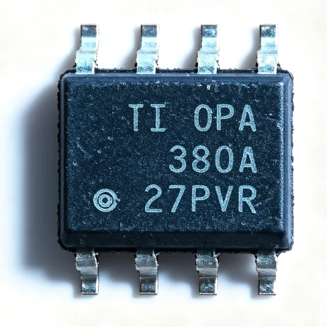
OPA380AID - 90MHz Precision Transimpedance Amplifier | TI
The Texas Instruments OPA380AID is a precision, high-speed transimpedance amplifier in an 8-pin SOIC (D) package, combining a 90MHz gain bandwidth product with extremely high DC precision for fast photodiode applications. It converts photodiode currents up to 1mA into voltage signals with transimpedance bandwidth exceeding 1MHz. A transimpedance amplifier (TIA) is a specialized current-to-voltage converter built on an operational amplifier with a feedback resistor, forming the analog front end of optical receivers, barcode scanners, and photodiode-based instruments. Within the signal-chain hierarchy, the TIA sits between the photodetector and the ADC or comparator, and its noise, bandwidth, and offset set the dynamic range of the whole optical link. Key features include 50pA maximum input bias current, 25uV maximum offset voltage, and 0.1uV/C maximum drift, giving 4 to 5 decades of dynamic range. The very low 1/f noise and excellent long-term Vos stability result from an internal auto-zero amplifier cascaded with a high-speed amplifier, rather than a traditional composite approach, improving overload recovery and settling time. The auto-zero plus high-speed composite architecture eliminates the usual precision-versus-speed trade-off: DC accuracy typical of chopper amplifiers is retained while delivering >1MHz transimpedance bandwidth. Quiescent current is 6.5mA per amplifier. Typical applications include high-speed photodiode receivers for optical communications, laser rangefinders and LiDAR receivers, barcode and medical CT scanner photodiode front ends, and precision optical power meters. For stable operation, keep the photodiode capacitance and feedback resistor within the datasheet stability region; a small feedback capacitor is usually required, and the output may need a pull-down resistor to include 0V in the output swing.

OPA380AID - 90MHz Precision Transimpedance Amplifier | TI
The Texas Instruments OPA380AID is a precision, high-speed transimpedance amplifier delivered in an 8-pin SOIC package. It combines a 90MHz gain bandwidth (GBW) with extremely high DC precision, providing transimpedance bandwidth above 1MHz for photodiode currents up to 1mA. A transimpedance amplifier (TIA) is a specialized operational amplifier circuit that converts a sensor current, most commonly from a photodiode, into a proportional output voltage. Within the signal-chain hierarchy, the TIA sits between the optical or current-output sensor and the ADC or comparator, and its bandwidth, input bias current, and offset voltage set the system's dynamic range. The OPA380 belongs to the wider family of precision amplifiers and analog front-end ICs in power management of optical receivers. Key features include a maximum input bias current of 50pA, a maximum offset voltage of 25uV with only 0.1uV/degC drift, and 4 to 5 decades of dynamic range. These specs allow direct interface with high-impedance photodiodes without external cancellation circuitry. Architecturally, the OPA380 results from an internal auto-zero amplifier combined with a high-speed amplifier. This composite topology delivers very low 1/f noise and excellent long-term VOS stability while TI's design improves overload recovery and settling time over a traditional discrete composite approach. Typical applications include high-speed photodiode receivers for optical data links, photodiode-based instrumentation such as spectrophotometers and lab photoreceivers, and barcode or LiDAR-style pulse detection where >1MHz transimpedance bandwidth matters. Design tip: the feedback resistor and photodiode capacitance set stability - use the datasheet's feedback capacitor guidance, and note the output swings to within millivolts of ground only on a single supply with load returned to a negative rail or virtual ground.
OPA388ID - 10 MHz Zero-Drift Precision Op Amp | Texas Instruments
The Texas Instruments OPA388ID is a single, 10 MHz, CMOS, zero-drift, zero-crossover, true rail-to-rail input/output precision operational amplifier in an 8-SOIC package. It combines a 0.25 µV offset with 0.005 µV/°C temperature drift, making it suitable for precision analog signal chains where dc accuracy and low-frequency noise are more important than wideband performance alone. A zero-drift operational amplifier is a precision amplifier architecture that continuously corrects its input offset voltage to reduce temperature-dependent drift. The OPA388 family combines this behavior with zero-crossover operation, low-noise performance, fast settling, and true rail-to-rail input and output capability. It belongs to the broader hierarchy of operational amplifier, analog amplifier, analog IC, and semiconductor devices. The OPA388ID offers 10 MHz gain-bandwidth performance and true rail-to-rail operation at its input and output. Its 0.25 µV offset specification supports accurate sensing of low-level signals, while the 0.005 µV/°C drift specification improves stability across changing ambient temperatures. These characteristics make the device useful in precision measurement, current sensing, sensor interfaces, and buffered analog systems where conventional amplifiers can introduce significant low-frequency error. The CMOS implementation and zero-crossover architecture are intended to reduce distortion during input and output signal transitions. Rail-to-rail input operation permits the common-mode input range to extend close to the supply rails, while rail-to-rail output operation increases usable output swing. The result is a precision amplifier that can operate directly from low-voltage supplies without sacrificing input range or output headroom. Typical applications include precision bridge and strain-gauge signal conditioning, buffered sensor outputs, low-level current measurement, laboratory instrumentation, industrial measurement systems, and analog-to-digital converter input drivers. The OPA388 is especially useful when the signal of interest is small, slowly varying, or monitored over a broad temperature range and requires the amplifier's offset and drift characteristics rather than maximum bandwidth. When designing around the OPA388ID, evaluate the complete signal path rather than the amplifier alone. Sensor excitation, reference voltage, resistor-network tolerance, input bias current, source impedance, ADC input range, and thermal gradients all contribute to system error. Stable layout, careful grounding, appropriate bypass capacitance, and attention to leakage or thermoelectric effects are necessary to preserve the precision promised by the low-offset device. This page combines manufacturer specifications with package, sourcing, application, and design guidance for engineers evaluating the OPA388ID. It also distinguishes confirmed device characteristics from parameters that require the manufacturer datasheet or a current distributor quotation, helping support faster component selection and more reliable PCB design decisions.

OPA396 - 1MHz 24uA Precision RRIO Op Amp | Texas Instruments
The Texas Instruments OPA396 is a single, micropower precision operational amplifier featuring rail-to-rail input and output (RRIO) operation. It combines a 1 MHz gain-bandwidth product with an ultra-low quiescent current of 23.5 uA (24 uA typ), packaged in the tiny SC-70-5 (DCK) surface-mount package for space-constrained portable designs. An operational amplifier (op amp) is a high-gain voltage amplifier with differential inputs and a single-ended output, and is a fundamental building block of analog signal conditioning used for amplification, filtering, and buffering. The OPA396 belongs to the precision op amp category, which prioritizes low offset voltage, low drift, and low input bias current. Within the amplifier hierarchy it is a micropower precision op amp, positioned between general-purpose op amps and ultra-low-power nanopower devices, and its RRIO capability maximizes dynamic range in low-voltage systems. Key differentiating specifications include an ultra-low input bias current of 10 fA (CMOS input stage), a maximum offset voltage of 100 uV, and a low offset drift of 1.2 uV/C over temperature. These parameters deliver high DC accuracy in sensor interfaces and transimpedance applications. The device operates from a 1.7 V to 5.5 V single supply and is specified from -40C to +125C, supporting both single-cell battery systems and industrial environments. Technically, the OPA396 uses a CMOS input stage responsible for its femtoampere-level bias current, and a class-AB rail-to-rail output stage providing solid drive at low supply current. Its high speed-to-power ratio (1 MHz bandwidth at 23.5 uA) is exceptional for battery-powered equipment, and unity-gain stability simplifies design-in. It is a member of the OPAx396 family, which includes single (OPA396), dual (OPA2396), and quad (OPA4396) versions for scalable designs. Typical applications include battery-powered instrumentation, photodiode transimpedance amplification where the 10 fA bias current minimizes dark-current error, portable medical devices, and low-power active filters. The rail-to-rail output swings fully at 1.7 V supplies, allowing direct interfacing with ADCs in IoT sensor nodes and wearable electronics. For design-in, decouple the supply with a 0.1 uF capacitor placed close to the supply pin, and account for the noise-gain versus bandwidth trade-off in high-gain configurations. Prices as of 2026-08-30 reflect distributor single-unit and volume pricing shown below.

OPA404AG - 6.4MHz Precision Quad Op Amp | Texas Instruments
The Texas Instruments OPA404AG is a four-channel, high-speed precision DiFET operational amplifier with 6.4 MHz gain-bandwidth product, 35 V/us slew rate, and ±750 uV maximum input offset voltage. The OPA404AG is supplied in a 14-CDIP package and is specified for operation from a minimum total supply of 10 V to a maximum total supply of 36 V. An operational amplifier is an analog integrated circuit that amplifies the voltage difference between its two inputs while using negative feedback to control gain and bandwidth. The OPA404 belongs to the precision operational-amplifier hierarchy, which includes voltage-feedback amplifiers, analog signal-chain ICs, and broader semiconductor devices. Its input-cascode architecture combines precision input characteristics with high-speed performance, while its standard quad pin configuration allows four amplifiers to be used in one package. Key features include a 6.4 MHz wide bandwidth, 35 V/us high slew rate, ±750 uV maximum offset voltage, and ±4 pA maximum bias current. The amplifier is unity-gain stable, allowing direct use in voltage-follower configurations without a frequency-compensation network. Its specified 0.01% settling performance supports precise, high-speed feedback systems where waveform accuracy must be maintained after a transition. The DiFET input stage and input-cascode design are central to the OPA404's performance. The cascode arrangement supports high precision input specifications while preserving wide bandwidth and rapid slew performance. With four independent channels in one package, the device can implement matched amplifier functions, current-feedback paths, instrumentation circuits, active filters, or general-purpose analog signal conditioning where one package per channel is undesirable. Typical uses include precision signal conditioning, low-level sensor amplification, instrumentation, data-acquisition front ends, active filtering, and audio or communications circuits. Designers can use the unity-gain stability for voltage followers, or apply external feedback networks for inverting, non-inverting, and differential amplifier configurations. Care must be taken to maintain adequate phase margin, observe the supply-voltage limits, and account for input and output common-mode restrictions. When laying out a board, place each input, feedback component, and decoupling capacitor close to the corresponding amplifier pins. Use a stable low-noise reference for precision measurements, verify common-mode and output-swing limits at the selected supply voltage, and test the completed circuit for stability across the intended gain and frequency ranges. The ceramic-DIP package is mechanically larger than typical surface-mount alternatives, so board area and socket availability should be considered before design release. This page combines the manufacturer's key electrical characteristics with package information, application guidance, comparison parameters, and a conservative drop-in assessment. It also identifies where OPA404AG alternatives were not established, helping engineers distinguish a verified pin-compatible replacement from a merely similar amplifier.

OPA404KP - Quad Difet Op Amp 6.4MHz 35V/us | Texas Instruments
The Texas Instruments OPA404KP is a quad high-speed precision Difet operational amplifier delivering 6.4MHz bandwidth, 35V/us slew rate, and a maximum offset voltage of +/-750uV in a 14-pin PDIP package. Its input cascode architecture combines FET-class input bias current of +/-4pA maximum with uncompromised high-speed performance, making it one of the few quad precision amplifiers to merge these traits in a single DIP footprint. An operational amplifier (op amp) is a high-gain differential voltage amplifier used to perform analog signal conditioning tasks such as amplification, buffering, filtering, and integration. The OPA404 belongs to the precision amplifier hierarchy: operational amplifier -> precision JFET/Difet amplifier -> analog front-end IC. Quad devices integrate four matched amplifiers on one die, cutting board area and improving channel matching versus four single amplifiers. Key features include 6.4MHz gain-bandwidth, 35V/us slew rate, +/-4pA maximum input bias current, +/-750uV maximum offset voltage, and 0.01% settling performance. The Difet (dielectrically isolated FET) process yields input bias currents orders of magnitude below bipolar designs while retaining wideband dynamics, so the part serves both precision DC and fast AC signal paths simultaneously. The input cascode design maintains precision input specifications at high speed, unlike JFET parts such as the TL074 family, which trade precision for cost. Total supply voltage spans 10V to 36V, supporting +/-15V analog rails and single-supply operation from higher-voltage buses. The standard quad pinout allows direct upgrades of existing TL074/TL084 sockets to higher performance. Typical applications include data acquisition front ends, active filters, photodiode transimpedance amplifiers, and test instrumentation signal chains where four channels must share consistent precision characteristics. Design consideration: with 35V/us slew rate, layout and supply decoupling matter - place 0.1uF ceramic capacitors close to each supply pin, and watch output current limits when driving capacitive loads. This page synthesizes distributor pricing, drop-in alternatives, pinout data, and practical design notes not found in the manufacturer datasheet, as of 2026-09-13.

OPA404KU - Quad 6.4MHz Precision Difet Op-Amp | Texas Instruments
The Texas Instruments OPA404KU is a quad high-speed precision Difet (dielectrically-isolated FET) operational amplifier delivering 6.4 MHz bandwidth, 35 V/us slew rate, and a maximum input offset voltage of +/-750 uV, housed in a 16-pin SOIC package with the industry-standard quad op-amp pinout. A Difet operational amplifier is a precision op-amp built on dielectrically isolated FET process technology. Within the signal-chain hierarchy, the OPA404 belongs to the class of precision amplifiers: operational amplifier -> precision op-amp -> high-speed precision amplifier -> analog front-end IC. Unlike JFET-input op-amps fabricated on standard junction-isolated processes, Difet technology couples extremely low input bias current with wideband dynamics, a combination historically difficult to achieve in a single monolithic device. Key differentiating specifications include the 6.4 MHz wide bandwidth, 35 V/us high slew rate, +/-750 uV maximum offset voltage, +/-4 pA maximum input bias current, and 0.01% low settling time. This combination makes the device suitable when engineers need FET-input precision without sacrificing the speed of general-purpose high-speed amplifiers. Supply operation spans +/-5V to +/-18V (10 V to 36 V total), covering most analog instrumentation rails. Architecturally, the dielectrically isolated FET inputs contribute picoampere-level bias currents, which preserve accuracy when the amplifier is driven from high-impedance sources such as photodiodes, piezoelectric sensors, and high-value resistor networks. The standard quad pinout allows designers to drop the part into existing quad op-amp layouts originally designed around devices like the TL074 or TLC274, upgrading precision without PCB redesign. Typical applications include data acquisition front ends, precision integrators and active filters, photodiode transimpedance amplifiers, test and measurement instrumentation, and multi-channel audio or industrial signal processing where four matched channels in one package save board area and improve channel-to-channel matching. Design considerations: because input bias current is only a few picoamperes, use guard rings and clean board layout to prevent leakage paths from dominating the input error budget. Verify stability with capacitive loads and set gain appropriately for the 6.4 MHz bandwidth. This page synthesizes distributor pricing, verified alternatives, pinout data, and practical design notes not found in a single manufacturer datasheet, providing a one-stop engineering reference for the OPA404KU.

OPA404KU/1K - Quad 6.4MHz Precision Difet Op Amp | TI
The Texas Instruments OPA404KU/1K is a quad high-speed precision Difet (dielectrically-isolated FET) operational amplifier delivering 6.4 MHz bandwidth, 35 V/us slew rate, and +/-750 uV maximum offset voltage in a 16-pin SOIC (DW) package rated 0C to +70C. A precision operational amplifier is a differential-input, high-gain voltage amplifier built around a FET or bipolar input stage that minimizes DC error terms such as offset voltage and input bias current. Within the signal-chain hierarchy, op amps sit between sensors/ADCs and the wider analog front end, making their DC accuracy and dynamic performance critical to overall system precision. The Difet process uses dielectric isolation of the input FETs, which reduces input bias current far below what junction-isolated JFET processes achieve. Key features include an unusually low maximum input bias current of +/-4 pA, 0.01% settling to fast accuracy levels, unity-gain stability, and a standard quad op amp pinout that allows direct upgrading of existing designs. The combination of low bias current with wide bandwidth and fast slew rate in a single quad package is rare and eliminates matching multiple singles. Technically, the dielectrically isolated FET input stage keeps bias current low over temperature and input range, while the internal compensation guarantees stability down to unity gain without external capacitors. The standard quad pin configuration (outputs on pins 1, 7, 8, 14) preserves compatibility with legacy quad sockets. Typical applications include precision instrumentation, optoelectronics, sonar and ultrasound front ends, professional audio equipment, medical equipment, and detector arrays. Design consideration: as a quad device, ensure each amplifier channel has proper supply decoupling, and account for the 0C to +70C commercial operating range - the industrial-range variant OPA404KU/1KE4-grade equivalents should be evaluated for extended temperature designs. This page synthesizes distributor pricing, verified drop-in alternatives, pinout data, and practical design notes not consolidated in the manufacturer datasheet.
OPA404SG - Quad 6.4MHz Precision Difet Op Amp | Texas Instruments
The Texas Instruments OPA404SG is a quad high-speed precision Difet (dielectrically isolated FET) operational amplifier delivering 6.4 MHz bandwidth, 35 V/us slew rate, and a maximum input offset voltage of +/-750 uV in a 14-pin CDIP (ceramic dual-in-line) package. An operational amplifier is a high-gain differential voltage amplifier that forms the foundational building block of the analog signal chain, sitting within the broader hierarchy of linear amplifiers and amplifier ICs in power management and signal conditioning systems. Quad op amps integrate four independent amplifier channels on a single die, sharing supply pins while keeping inputs and outputs independent, which reduces board area and improves channel-to-channel matching in multi-channel analog designs. Key features of the OPA404 include a wide 6.4 MHz bandwidth, a fast 35 V/us slew rate, low input bias current of +/-4 pA max enabled by the Difet input cascode architecture, 0.01% settling to fast accuracy, and a standard quad op amp pin configuration that allows direct upgrading of existing designs. The Difet (dielectrically isolated FET) process eliminates the junction-isolation leakage and parasitic capacitance of conventional processes, combining precision input specifications with uncompromised high-speed performance. The input cascode design keeps the drain-source voltage of the input FETs constant, stabilizing input bias current over temperature and common-mode range while preserving bandwidth. The SG suffix denotes the military-grade temperature rating in a hermetic ceramic package, supporting extended-temperature operation where plastic packaging is unacceptable, such as defense and aerospace instrumentation. Typical applications include high-speed data acquisition front ends, active filters in test and measurement equipment, precision integrators, photodiode transimpedance amplifiers, and multichannel buffer stages in industrial instrumentation. The quad configuration is particularly efficient in filter topologies such as state-variable designs that require four amplifiers per channel set. Design consideration: although the 4 pA bias current permits very large feedback resistors, resistor values above approximately 10 megaohm should be evaluated against parasitic capacitance effects on stability; use short feedback traces and consider a small feedback capacitor. This page synthesizes distributor availability, drop-in alternative analysis, and practical design guidance beyond what the manufacturer datasheet provides.
OPA4137P - Quad 36V 1MHz FET Op Amp | Texas Instruments
The Texas Instruments OPA4137P is a four-channel, J-FET-input operational amplifier with rail-to-rail input capability, a 1 MHz gain-bandwidth product, and a 3.5 V/µs slew rate, packaged in a 14-pin PDIP. It operates from ±2.25 V to ±18 V, giving the device a 36 V maximum total supply range for precision analog signal-chain designs that require low input bias current and broad supply-voltage flexibility. An operational amplifier is a high-gain differential amplifier used to amplify voltage differences while providing feedback-defined gain, filtering, buffering, or signal conditioning. The OPA4137 belongs to the FET-input operational-amplifier family within the broader analog IC and power-management signal-chain hierarchy. Its four amplifiers share a common package while providing independent channels for instrumentation, converters, and active filtering. The OPA4137P uses low-input-bias-current J-FET input stages, making it suitable for high-impedance sources that would load conventional bipolar transistor inputs. The series documentation identifies input bias current around 10 pA, quiescent current around 120 µA per channel, and open-loop gain around 145 dB for applicable family configurations. The 1 MHz gain-bandwidth product supports moderate-bandwidth precision applications rather than high-speed video or RF signal chains. Each channel combines low-noise J-FET inputs with a 3.5 V/µs slew rate. The family is intended for low-cost and miniature applications where low bias current, low quiescent current, and compact implementation are important. Because all four channels are integrated into one 14-pin PDIP, designers can reduce external interconnections in multi-channel filters, sensor front ends, and signal-conditioning boards. Typical applications include low-frequency precision filters, current-to-voltage conversion, audio and instrumentation signal conditioning, sensor amplification, and analog control loops. It is particularly appropriate when source impedances are high enough that input bias current could create an unacceptable DC error. It is less suitable for demanding high-speed, high-output-current, or unity-gain-stable high-voltage applications without careful review of the complete electrical characteristics. For PCB implementation, place each bypass capacitor close to the associated supply pins, keep feedback components close to their channel pins, and provide a quiet ground reference. Avoid long high-impedance traces because leakage, contamination, and parasitic capacitance can degrade the low-bias-current advantage. Confirm output swing, input common-mode range, noise, distortion, and stability against the actual gain and load before releasing the design. This page combines manufacturer specifications, package and pin information, sourcing guidance, verified cross-reference results, and practical design notes. It also identifies where an alternative requires explicit engineering review rather than assuming that a similar amplifier function guarantees a board-level drop-in replacement.

OPA4137U - Quad 36V 1MHz FET Op Amp | Texas Instruments
Texas Instruments OPA4137U is a quad FET-input operational amplifier designed for low-cost instrumentation and precision signal-chain applications. The device supports a 36 V supply, operates with 1 MHz gain-bandwidth product, and provides four amplifiers in a 14-SOIC package. Its defining electrical characteristics include 5 pA low input bias current, 220 µA quiescent current per channel, and 94 dB open-loop gain. A FET-input operational amplifier is an analog signal-conditioning device that uses field-effect-transistor input stages to provide very low input bias current. Within the signal-chain hierarchy, the OPA4137U belongs to the operational amplifier, analog amplifier, and signal-conditioning IC categories. This low-bias architecture is particularly useful when the amplifier must measure weak currents or signals without loading the source appreciably. The OPA4137 family combines low-cost construction with precision-oriented performance. Its 5 pA input bias current reduces DC error when sensing high-impedance sources, while the 94 dB open-loop gain supports accurate closed-loop amplification. The 1 MHz gain-bandwidth product is suitable for general-purpose instrumentation operating below the amplifier's higher-frequency limits. A low quiescent current of 220 µA per channel also benefits compact and low-power systems. The quad configuration integrates four FET-input amplifiers into one package, reducing board area compared with four separate single or dual devices. The OPA4137U is supplied in the 14-SOIC package identified by Texas Instruments as suitable for surface-mount assembly. Its monolithic circuit architecture supports consistent operation across the four channels while providing common supply rails for compact analog front ends. Typical uses include precision current measurement, photodiode and sensor interfaces, laboratory instrumentation, audio signal conditioning, and low-frequency active filters. The very low bias current is especially advantageous for source impedances in the gigaohm range. The 1 MHz bandwidth also permits practical operation in audio-frequency and general signal-conditioning networks when appropriate feedback and stability components are selected. PCB design should preserve a low-impedance ground return and place compensation, feedback, and input components close to the relevant amplifier pins. Input bias-current error should be evaluated against source impedance, and unused channels should be configured according to the manufacturer datasheet rather than left floating. Supply bypassing should follow the datasheet guidance and place a ceramic capacitor close to the supply pins. This product page combines the Texas Instruments device description, ordering information, package details, and manufacturer datasheet with practical application guidance. It also distinguishes verified drop-in alternatives from related amplifier families, helping engineers make package, bandwidth, supply-voltage, and precision decisions before committing to a PCB revision.