Amplifier ICs
بەرهەمەکان (3,200+)

LM393TLX/NOPB - Dual 36V Comparator | Texas Instruments
Texas Instruments LM393TLX/NOPB is a dual general-purpose differential comparator with open-collector outputs, rail-to-rail input capability, and a supply-voltage rating of 2 V to 36 V. The device contains two independent comparator channels and is supplied in an 8-DSBGA package. It also provides a maximum input offset voltage of 2.0 mV, a typical input bias current of 250 nA, and a response time of approximately 700 ns. A differential comparator is an analog integrated circuit that compares two input voltages and changes its output state when the difference crosses a selected threshold. The LM393 belongs to the comparator hierarchy within the broader semiconductor and signal-conditioning categories. Its open-collector outputs can sink current while remaining in a high-impedance state when inactive, making the device useful for wired logic interfaces, threshold detection, and systems that require an external pull-up resistor. The LM393 provides two independent comparator elements in one package. Rail-to-rail input operation extends the usable common-mode input range toward the supply rails, while the 2 V to 36 V operating range supports low-voltage logic and higher-voltage industrial systems. Open-collector outputs support wired-AND operation and interface compatibility with CMOS, DTL, ECL, MOS, and TTL logic families. The low 250 nA input bias current reduces disturbance in high-impedance sensing circuits. Each channel compares an inverting input with a non-inverting input. The output transistor turns on when the non-inverting input is above the inverting input, subject to the comparator's specified offset and response characteristics. Because the output is open collector, an external pull-up resistor establishes the inactive logic level. This architecture adds a passive pull-up component but offers flexibility for wired logic, level translation, and relay-driving arrangements. Typical uses include monitoring a sensor against a reference voltage, detecting battery or power-supply thresholds, checking overvoltage and undervoltage conditions, and generating a digital status signal from an analog control loop. Industrial equipment, battery-powered systems, automotive-style monitoring circuits, and general-purpose logic interfaces can also use the two channels independently. Design the open-collector output with a pull-up resistor sized for the required sink current, rise time, and logic-family current. Keep the comparator inputs short and place them away from switching nodes and sources of high-current return paths. Confirm that the input and output currents remain within their specified limits and that the selected pull-up voltage is appropriate for the downstream logic. This product page combines manufacturer specifications, package information, application guidance, comparison parameters, and practical design considerations to support component selection and PCB implementation. It also identifies the limits of publicly documented drop-in substitution for this exact 8-DSBGA ordering configuration.

LM4871MX/NOPB - 3W Mono Class-AB Audio Amp | Texas Instruments
The LM4871MX/NOPB is a mono bridged audio power amplifier from Texas Instruments, part of the Boomer series, capable of delivering 3W of continuous average power into a 3Ω load with less than 10% THD when powered by a 5V supply. It operates from a 2V to 5.5V supply, making it ideal for battery-powered portable devices. The device features a shutdown mode that reduces quiescent current to minimize power consumption when not in use. Housed in an 8-pin SOIC (D) package, it is designed for surface-mount assembly and operates over a temperature range of -40°C to 85°C. An audio power amplifier is an electronic amplifier that amplifies low-power audio signals to a level suitable for driving loudspeakers. The LM4871 is a Class-AB amplifier, which offers a good compromise between efficiency and linearity, providing low distortion while consuming moderate power. In the hierarchy of audio electronics, it falls under audio amplifiers, which are a subset of analog ICs used in consumer electronics, portable devices, and multimedia systems. Key features include a shutdown mode with low quiescent current (6.5mA typical), a wide supply voltage range of 2V to 5.5V, and a maximum output power of 3W into 3Ω. The device also offers thermal shutdown protection and is available in a lead-free (NOPB) version, compliant with RoHS. Its differential output architecture eliminates the need for output coupling capacitors, reducing external component count and board space. The LM4871 uses a bridged-tied load (BTL) configuration, which effectively doubles the voltage swing across the load compared to a single-ended amplifier, maximizing output power without increasing supply voltage. This architecture, combined with a low-noise design, ensures clean audio reproduction. The device is designed for simplicity, requiring only a few external components, making it easy to integrate into compact designs. Typical applications include portable speakers, mobile phones, MP3 players, and other battery-powered audio devices where high efficiency and low power consumption are critical. Its small SOIC package and minimal external component requirement make it suitable for space-constrained designs. When designing with the LM4871, ensure proper PCB layout with adequate ground plane and decoupling capacitors close to the supply pins to minimize noise and improve thermal performance. The shutdown pin can be used for power management to extend battery life.

LM4875M/NOPB - 750mW Mono Audio Amplifier w/ DC Volume | TI
The Texas Instruments LM4875M/NOPB is a 750 mW mono bridged audio power amplifier with DC voltage volume control and headphone switch, housed in an 8-pin SOIC package. It operates from a 2.7 V to 5.5 V supply, delivers 750 mW continuous average power into an 8 ohm load at less than 1% THD+N when powered from 5 V, and integrates a mono Class-AB output stage with a dedicated single-ended headphone channel. The die combines the speaker amplifier, headphone amplifier, depop circuitry, and a digitally-controlled analog volume interface in a single 8-pin SOIC footprint. An audio power amplifier IC is an integrated circuit that delivers sufficient low-distortion current to drive a loudspeaker or headphone transducer from a low-voltage analog source. Within the power management hierarchy, the LM4875M/NOPB belongs to the analog amplifier family, which is a sub-category of signal-chain ICs alongside op-amps, line drivers, and codecs. Class-AB amplifiers such as the LM4875 bias their output transistors with a small quiescent current, achieving higher efficiency than Class-A designs while avoiding the crossover notch distortion of Class-B push-pull stages. The bridged (BTL) topology doubles the voltage swing across the load without requiring a DC blocking capacitor or split supply, simplifying single-rail portable designs. Key features of the LM4875M/NOPB include 750 mW output into 8 ohm at 5 V with 0.5% THD+N, an integrated DC voltage volume control pin that sets gain in 32 steps, an automatic bridged-mode / headphone-mode sense pin, click-and-pop suppression on enable and mode transitions, and thermal shutdown protection. The supply range of 2.7 V to 5.5 V supports both single-cell Li-ion (3.7 V nominal) and USB-powered (5 V) rails, making the part well suited to handheld consumer audio. The 8-pin SOIC (M) package is JEDEC MS-012 standard with a thermal pad absent, so most dissipation is handled through the PCB copper pours on pins 4 and 5. The device uses a fully differential Class-AB output stage with internal feedback networks, plus a switched headphone amplifier that engages when a jack is sensed. Volume is set by a DC voltage on the VOL pin rather than a logarithmic taper potentiometer, eliminating the need for a mechanical pot and allowing software or hardware mute. The depop circuit controls the output common-mode voltage during power-up and headphone insertion, suppressing the audible transient that plagues many low-cost amplifiers. Typical applications include portable media players, USB-powered speakers, MP3 docking stations, laptop and tablet audio outputs, point-of-sale and kiosk audio prompts, and intercom / doorbell audio. The wide 2.7-5.5 V supply range and small 8-pin SOIC footprint make it a strong fit for any battery- or bus-powered design that needs more volume than a codec headphone amp can deliver. When designing with this part, ensure the input coupling capacitors are sized for the lowest desired bass response (47 nF gives roughly -3 dB at 300 Hz into the internal 20 kohm input impedance). Provide adequate ground copper on pins 4 and 5, and keep the HP-SENSE trace short to avoid false mode switching. This page synthesizes DigiKey/Mouser distributor pricing, drop-in same-package alternatives, and application-specific design notes not aggregated in the manufacturer datasheet, giving engineers a faster path to a verified BOM.

LM7321MFX/NOPB - 32V 20MHz RRIO Op Amp SOT-23-5 | TI
The Texas Instruments LM7321MFX/NOPB is a single-channel, rail-to-rail input and output (RRIO) operational amplifier delivering 20-MHz unity-gain bandwidth, 18-V/us slew rate, and up to 65 mA of output current from a compact 5-pin SOT-23 (DBV) package. It operates from supplies of 2.5V to 32V (up to +/-16V dual supply) while drawing only about 1 mA of supply current per amplifier. An operational amplifier (op amp) is a high-gain voltage amplifier used in the analog signal chain hierarchy: amplifier IC -> general-purpose op amp -> precision analog front end. The LM7321 belongs to the rail-to-rail op amp class, whose input and output stages swing to within millivolts of both supply rails, maximizing dynamic range in low-voltage and single-supply systems. Key differentiating features include unlimited capacitive load stability - the output drives large capacitive loads directly without external compensation - plus the high 65-mA output current that allows the device to drive heavy loads such as coaxial cables, ADC inputs, and actuator drivers. The rail-to-rail I/O architecture maintains performance across the full 2.7V, +/-5V, and +/-15V operating points specified by TI, and the wide temperature range of -40C to +125C supports industrial and automotive-adjacent designs. Internally, the LM732xx family uses a complementary input stage that seamless transfers near the rails, preserving bandwidth and phase margin across the common-mode range. The combination of 20-MHz bandwidth with only 1-mA quiescent current yields an excellent bandwidth-to-power figure compared with general-purpose parts such as the LM358. Typical applications include video and coaxial cable drivers, ADC input buffering, active filters, piezo and capacitive load drivers, test-and-measurement signal conditioning, and battery-powered portable instrumentation. The NOPB suffix indicates RoHS-compliant, lead-free terminations. Design tip: while capacitive load stability is essentially unlimited, keep supply decoupling close to the pins (100 nF per rail) and beware of thermal limits when sourcing 65 mA continuously at high output voltage swing.
LM741-MIL - General-Purpose Operational Amplifier | Texas Instruments
The Texas Instruments LM741-MIL is a general-purpose operational amplifier intended for a wide range of analog applications. Its verified product information identifies improved performance over industry standards such as the LM709, while the listed package and detailed electrical values are not supplied in the retrieved web data. The device is associated with the LM741 series, a classic single-amplifier architecture used in integrator, summing-amplifier, and general-feedback circuits. An operational amplifier is an integrated circuit that uses high-gain differential amplification with negative feedback to create predictable closed-loop behavior. The LM741 family belongs to the broader operational-amplifier, analog-amplifier, signal-conditioning, and semiconductor categories. Its general-purpose positioning makes it relevant to educational circuits, laboratory instruments, audio signal paths, analog control systems, filters, amplifiers, and legacy equipment where an established 741-family pinout and application ecosystem may be important. According to the verified Texas Instruments product-page information, the LM741-MIL provides improved performance relative to the LM709 and is a direct plug-in replacement for the 709C, LM201, MC1439, and 748 in most applications. The same source states that its high gain and wide operating-voltage range support integrator, summing-amplifier, and general-feedback applications. Exact supply voltage, input common-mode range, output swing, gain-bandwidth product, slew rate, input bias current, offset voltage, noise, and temperature-range values are not included in the supplied evidence and therefore must be verified from the manufacturer datasheet before design use. The verified Mouser result further describes the LM741-MIL as an operational amplifier for wide-ranging analog applications. The retrieved sources also identify the manufacturer as Texas Instruments and provide links to the product page and datasheet. Because the supplied data does not establish a precise orderable package suffix, pin count, lead-free status, automotive qualification, lifecycle classification, or distributor price, those fields remain data-needed rather than inferred. Typical circuit uses include closed-loop non-inverting and inverting amplifiers, analog summing networks, active filters, integrators, transducers, and general feedback control blocks. Designers should preserve the package and pinout of the installed circuit, confirm the applicable electrical limits, and verify stability, biasing, output swing, and compensation requirements before substituting a modern amplifier. This page summarizes only verified web information and avoids adding undocumented electrical claims. For a new high-precision design, compare the LM741-MIL against modern rail-to-rail input and output amplifiers, because the LM741’s historical architecture is not automatically the best choice for low-voltage or high-speed systems. For an existing legacy board, use the verified direct-plug-in-replacement claim only after checking the exact package and pin arrangement against the current schematic and datasheet.
LM741C - General-Purpose 0.9 MHz Op Amp | Texas Instruments
The Texas Instruments LM741C is a general-purpose, single operational amplifier with a 0.9 MHz gain-bandwidth product, specified for operation from 0°C to +70°C, and supplied in an 8-pin package. It provides high open-loop gain, short-circuit protection, and latch-free operation for legacy analog designs. The supplied data does not identify one orderable package suffix, so the verified data references both TO-5 and PDIP variants; confirm the exact suffix before ordering or replacement. An operational amplifier is an analog integrated circuit that uses very high open-loop gain to amplify the difference between its inverting and non-inverting inputs. Negative feedback shapes the closed-loop gain, bandwidth, and impedance behavior. Within the broader hierarchy of semiconductor, analog IC, and amplifier, the LM741C is a mature general-purpose voltage-feedback amplifier commonly used where cost, tolerance of older systems, and broad compatibility matter more than low offset, low noise, rail-to-rail operation, or high speed. Key verified attributes include a 0.9 MHz bandwidth designation, high gain, short-circuit protection, and latch-free operation. The LM741C is described by Texas Instruments as identical to LM741 and LM741A except that its performance is ensured over 0°C to +70°C instead of -55°C to +125°C. This makes it appropriate for commercial-temperature legacy equipment, but not automatically acceptable where an automotive, military, or full industrial temperature rating is required. The architecture is the classic single-supply operational-amplifier approach associated with the LM741 family. Its inverting input receives feedback, its non-inverting input receives the source signal, and offset-null pins can support external adjustment where required. Unlike modern rail-to-rail, zero-crossover input-stage amplifiers, designers must preserve suitable common-mode headroom and provide adequate supply voltage. Input bias current, input offset voltage, slew rate, supply current, and maximum output swing require confirmation from the manufacturer datasheet before precision or load-dependent calculations. Typical applications include educational amplifier laboratories, basic active filters, audio preamplification, sensor-conditioning stages, instrumentation interfaces, power-control loops, and repair of vintage analog equipment. For a non-inverting amplifier, the closed-loop gain is normally set by external resistors; for an inverting amplifier, the signal enters the inverting terminal and feedback defines the gain. Component tolerances and bias-current compensation must be checked before claiming high accuracy. The principal design caution is not to assume that any pin-compatible amplifier is electrically interchangeable. Input topology, common-mode range, offset-null implementation, output swing, supply limits, noise, bandwidth, and stability differ among modern alternatives. Use a replacement only after comparing the exact package pinout and full operating envelope. If the PCB uses DIP-8, an SOIC-8 replacement is not drop-in and requires layout changes. This page combines the verified Texas Instruments and distributor-hosted LM741C information with package-qualified replacement guidance and practical integration notes. It distinguishes documented facts from missing orderable-suffix data, helping engineers locate the datasheet, assess legacy use, and request a quotation without treating generic amplifier equivalences as guaranteed drop-in parts.

LM759CH - Power Operational Amplifier in TO-99 | Texas Instruments
The Texas Instruments LM759CH is a single-circuit power operational amplifier in an 8-pin TO-99 metal can package. The verified product record identifies it as an amplifier IC from the original National Semiconductor power-operational-amplifier family, while the Rochester listing describes the device as the LM759 power operational amplifier in MBCY8. Its principal role is to provide higher output current and drive capability than a conventional small-signal operational amplifier. An operational amplifier is a high-gain analog building block used to amplify voltage differences. A power operational amplifier adds output-current capability so it can drive heavier loads, including audio transducers, motors, lamps, and other low-impedance or high-current external circuits. In system terminology, the LM759CH belongs to the operational-amplifier hierarchy and analog-signal-chain category rather than to a general-purpose digital IC. The supplied distributor information confirms the LM759CH identity, single amplifier circuit count, TO-99-8 package description, power-operational-amplifier classification, and the availability of datasheet and pricing resources. The verified snippets do not provide a complete electrical parameter table. Consequently, specifications such as supply voltage, output-current capability, gain-bandwidth product, slew rate, input offset, noise, thermal resistance, and operating-temperature range remain explicitly marked as needing verification rather than inferred from related devices. Typical uses suggested by the LM759 family description include audio output stages, motor or actuator drivers, lamp drivers, laboratory output stages, and industrial control interfaces. In these applications, the important design checks are supply headroom, output-current margin, thermal dissipation, stability with the intended load, and protection against shorts or capacitive loads. The metal-can package provides a thermal path, but the actual junction temperature still depends on the board, ambient temperature, lead length, load, and power dissipation. Use the manufacturer or authorized distributor datasheet as the controlling document before layout or production substitution. Verify the exact pinout, compensation requirements, output-stage limits, common-mode range, and recommended external components for the specific LM759CH variant. Rochester documentation may describe a manufactured or supported legacy configuration, so its specifications should not be merged with a different TI orderable variant without comparison. This page combines verified distributor listings, a genuine datasheet link, practical application guidance, and explicit data gaps rather than inventing missing electrical values. It is intended to support initial sourcing and engineering triage while preserving traceability to the available records.
LM759MH - Military 8-Pin Power Op Amp | Texas Instruments
The Texas Instruments LM759MH is a military-temperature, single power operational amplifier packaged in an eight-terminal round metal can. The verified distributor data identifies it as a power operational amplifier with an 8-terminal wire-lead package; further electrical ratings were not supplied. Its established role is signal conditioning where a relatively high-capability power amplifier can drive heavier external loads than ordinary small-signal operational amplifiers. An operational amplifier is a high-gain analog semiconductor that compares two input voltages and drives its output toward the condition that minimizes their difference. In the broader electronics hierarchy, an operational amplifier belongs to analog ICs, amplifiers, and signal-conditioning components. Depending on compensation, stability, supply, output-stage, and package requirements, an LM759MH circuit may support inverting, non-inverting, comparator-like, or feedback-controlled amplifier configurations. The LM759 designation identifies a historical power operational-amplifier family from National Semiconductor, now associated with Texas Instruments. Verified listings describe LM759MH as a military-temperature part. One distributor record also identifies the package as an 8 metal can package and classifies the terminal finish as tin lead, making exact procurement, assembly, and soldering-process review important before use in a new design. Typical power-amplifier uses include motor or actuator drive, audio output stages, laboratory buffer circuits, and industrial control blocks where source-level op amps may lack adequate output-current capability. These applications cannot be qualified without the missing electrical specifications, especially supply voltage, output-current limit, output swing, slew rate, gain-bandwidth product, offset voltage, bias current, noise, and thermal limits. Engineering use of LM759MH should begin with the manufacturer or archived National Semiconductor datasheet, followed by explicit stability and load testing. Confirm the pinout, compensation method, common-mode limits, output drive, maximum supply, temperature grade, and thermal behavior before laying out a board. Do not substitute a generic eight-pin amplifier solely by package count; topology, voltage ratings, output-stage architecture, and compensation can be incompatible. This page consolidates the verified LM759MH package, temperature-grade, sourcing, and datasheet information with explicit engineering cautions. Because the supplied search evidence does not include numerical performance tables or qualified replacement MPNs, unknown technical values are marked rather than guessed, preserving traceability for military, industrial, and legacy-system evaluation.

LM833MMX/NOPB - Dual Audio Op-Amp 15MHz 8-VSSOP | Texas Instruments
The Texas Instruments LM833MMX/NOPB is a dual high-speed audio operational amplifier in an 8-pin VSSOP (Mini Small Outline Package) tape-and-reel variant, delivering 15 MHz unity-gain bandwidth with low distortion and low noise optimized for audio and data-signal applications. The device features two independent op-amps with high slew rate, high gain bandwidth product, and operates from ±5 V to ±15 V dual supplies (or 5 V to 30 V single supply), making it suitable for both consumer audio and professional signal-conditioning designs. The 8-VSSOP (DGK) package supports compact PCB layouts where board area is at a premium. An audio operational amplifier is a specialized op-amp engineered with input bias-current, noise, and distortion characteristics optimized for audio frequency band (20 Hz to 20 kHz) signal chains. Within the broader taxonomy, the LM833 belongs to the linear amplifier family, which sits under operational amplifiers (op-amps), under analog ICs, under signal conditioning, under semiconductors. The dual op-amp topology integrates two amplifiers in a single package, enabling stereo signal chains, balanced line receivers, and active filters with matched performance between channels. Key features include 15 MHz unity-gain bandwidth, 7 V/us slew rate, low input voltage noise density of 4.5 nV/sqrt(Hz), and an input bias current of 300 nA maximum. The device offers high-gain bandwidth product (GBW), wide supply range (5 V to 30 V single, ±2.5 V to ±15 V dual), and is unity-gain stable. The MMX suffix denotes the 8-pin MSOP/VSSOP package on tape-and-reel (TR), while the standard MM (without X) ships in tubes. Drop-in compatibility with the LM833MM/NOPB in the same 8-VSSOP (DGK) package is preserved across all electrical specifications. The LM833 utilizes a bipolar transistor input stage and a JFET-free architecture, achieving low-noise performance suitable for microphone preamplifiers, active crossovers, and high-fidelity audio DAC output buffers. The wide gain-bandwidth product supports AC-coupled audio stages where the op-amp must preserve signal integrity at high frequencies beyond the audible band, ensuring minimal harmonic and intermodulation distortion. Typical applications include stereo audio preamplifiers, microphone preamps, active equalizers, audio mixers, headphone drivers, and instrumentation amplifiers. The dual-channel configuration also enables balanced line receivers and differential active filters in both pro-audio and prosumer equipment. When designing with this device, observe proper power-supply decoupling with a 0.1 uF ceramic capacitor placed within 5 mm of each supply pin. The high GBW requires attention to PCB layout to minimize parasitic capacitance at the inverting input; ground plane management and short, direct signal traces are recommended. This page synthesizes distributor pricing, same-brand and cross-brand drop-in alternatives, and practical design notes not found in the manufacturer datasheet alone, helping engineers select and qualify LM833MMX/NOPB more efficiently.

LM842 - CMOS RRIO Wide-Supply Dual Op-Amp | Texas Instruments
The Texas Instruments LM842 (LMV842) is a dual CMOS-input, rail-to-rail input/output (RRIO) operational amplifier with near-precision specifications, 4.5 MHz gain-bandwidth product, and a wide 2.7 V to 12 V supply range. Housed in 8-pin VSSOP (DGK) and 8-pin SOIC (D) packages, the LM842 integrates two independent amplifiers on a single die, with low noise (typically 12 nV/sqrt(Hz)), low input offset voltage (LMV841/2/4 family), low offset drift, and low quiescent current per channel. A CMOS operational amplifier (op-amp) is a high-gain DC-coupled analog building block whose differential inputs and single-ended output form the foundation of signal conditioning. The RRIO family extends usable signal swing to within millivolts of either supply rail - critical for modern low-voltage single-supply systems. Within the broader power management and analog hierarchy, op-amps sit alongside voltage regulators, references, and ADCs as core signal-chain components that convert, scale, filter, and buffer analog signals before digitization or further amplification. Key features of the LM842 include 4.5 MHz unity-gain bandwidth, 1.3 V/us slew rate, 12 nV/sqrt(Hz) input voltage noise density, RRIO swing on both input and output stages, and a 2.7 V to 12 V supply range that accommodates 3.3 V, 5 V, and 12 V rails without level shifting. The CMOS input stage presents pA-level bias current, eliminating the bias-current errors common to bipolar and JFET op-amps in high-impedance sensor interfaces. The architecture uses a complementary CMOS input differential pair with a rail-sensing output stage, achieving true rail-to-rail output swing at loads up to several mA. The wide supply range and low quiescent current (typically 0.4 mA per channel) make the device attractive for both line-powered and portable equipment. Typical applications include active filters, transducer amplifiers, battery-powered instrumentation, portable audio buffers, and general-purpose signal conditioning for sensor front ends. Designers should note that the dual-package 8-pin pinout shares the industry-standard SOIC-8/VSSOP-8 dual op-amp footprint, enabling direct drop-in substitution with pin-compatible parts from multiple vendors. This page synthesizes distributor pricing, parametric alternatives, and practical design guidance beyond the manufacturer datasheet.

LME49600TS/NOPB - 110MHz High-Current Headphone Buffer | TI
The Texas Instruments LME49600TS/NOPB is a 1-channel, high-fidelity, high-current audio headphone buffer housed in a TO-263 (DDPAK-5) package. It delivers a 110 MHz bandwidth in low-current mode and an extended 180 MHz bandwidth in wide-bandwidth mode, with a nominal 2000 V/us slew rate that preserves transient fidelity in demanding audio paths. The output stage can swing ±7.5 V and source/sink up to ±250 mA, making it suitable as a high-current output stage for headphone amplifiers, line drivers, and operational-amplifier booster stages. A buffer is a unity-gain (or near unity-gain) current amplifier that sits between a low-power op-amp or DAC output and a low-impedance load. Buffers multiply the available drive current without significantly altering voltage gain, and they are categorized within the broader hierarchy of operational amplifiers -> amplifiers -> analog signal-chain ICs. The LME49600 specifically addresses high-fidelity audio where the combination of wide bandwidth, high slew rate, and high output current into 32 ohm headphones is critical to preserving waveform integrity. Key features include pin-selectable bandwidth (7.3 mA quiescent current at 110 MHz versus 13.2 mA at 180 MHz), low total harmonic distortion plus noise, an enable/disable pin, and a wide ±2.25 V to ±18 V dual supply range. The DDPAK-5 power package with an exposed thermal pad supports the high continuous dissipation required when driving low-impedance loads, while the small surface-mount footprint simplifies PCB integration in space-constrained audio products. The LME49600 is built on a bipolar complementary (push-pull) output architecture optimized for high-current linear operation. The internal design minimizes crossover distortion and offers a high slew rate that preserves square-wave and high-frequency music content. Designers can place the LME49600 inside or outside an op-amp's feedback loop, enabling flexible topology choices from simple buffers to composite amplifiers with substantially higher output current than the host op-amp alone. Typical applications include headphone amplifiers for studio monitors and audiophile consumer gear, professional line drivers for mixing consoles, op-amp current boosters for ADC drivers, audio DAC output stages, and test-and-measurement instrumentation requiring low-distortion high-current signal delivery. When designing with the LME49600, pay attention to PCB thermal management. Estimated: at a 12 V supply driving 32 ohm headphones at full ±7 V swing, continuous dissipation in the TO-263 package may exceed 1 W, so a copper pour and thermal vias under the exposed pad are mandatory for reliability.
LMH6624MAX/ - 1.5GHz Low Noise Op Amp | Texas Instruments
The Texas Instruments LMH6624MAX/ is a single-channel, ultra-low-noise, wideband voltage-feedback operational amplifier housed in an 8-pin SOIC (MAX package suffix) that delivers 1.5 GHz gain-bandwidth product, 0.92 nV/√Hz input voltage noise density, and 2.3 pA/√Hz input current noise density. The amplifier combines this wideband AC performance with low DC errors including 100 µV typical input offset voltage and ±0.1 µV/°C drift, enabling closed-loop gains above 10 in both inverting and non-inverting configurations. It operates from ±2.5 V to ±6 V dual supply or 5 V to 12 V single supply. A voltage-feedback op amp is a class of analog amplifier whose closed-loop bandwidth is set by the feedback network rather than the op amp's internal gain, allowing designers to trade gain for bandwidth. Voltage-feedback amplifiers (VFAs) sit within the broader operational amplifier hierarchy, which includes current-feedback amplifiers (CFAs), instrumentation amplifiers, and precision chopper-stabilized amplifiers. The LMH6624 family targets wideband precision signal chains where low noise and low DC error must coexist at high frequency. Key features include 1.5 GHz gain-bandwidth, 0.92 nV/√Hz input noise, 2.3 pA/√Hz current noise, 100 µV VOS, ±0.1 µV/°C drift, 1500 V/µs typical slew rate, and 70 mA output current. The wide supply range supports ±2.5 V to ±6 V dual or 5 V to 12 V single-supply operation. The SOIC-8 surface-mount package offers a thermal resistance around 150 C/W and supports -40 °C to +125 °C ambient operation. The device uses a bipolar transistor input stage and complementary bipolar output stage, allowing rail-to-rail output swing within ~0.7 V of either supply. The architecture balances voltage noise and current noise favorably for source impedances in the 1 kΩ to 50 kΩ range, which is the sweet spot for photodiode transimpedance, ADC buffers, and ultrasonic preamps. Typical applications include photodiode transimpedance amplifiers, ultrasonic preamps, IF/RF signal-chain buffers, high-speed ADC input drivers, active filters, and precision instrumentation front-ends. In transimpedance applications, the combination of 0.92 nV/√Hz and 2.3 pA/√Hz noise is critical when the photodiode capacitance and feedback resistor push the noise optimum into this impedance window. When designing, keep feedback resistor values low to limit noise gain peaking, use a small feedback capacitor to stabilize the loop, and place supply-bypass capacitors within 2 mm of the V+ and V- pins. Output drive is rated to ±70 mA but sustained DC output current near this value will heat the SOIC-8 package quickly - derate or use the SOIC-8 EP variant for heavier loads. This page synthesizes distributor pricing, drop-in alternatives, and design notes not found in the manufacturer datasheet, giving engineers a one-stop specification and selection resource.
LMP7721MA/NOPB - 3fA Bias Precision Op Amp 17MHz | TI
The Texas Instruments LMP7721MA/NOPB is a precision operational amplifier featuring the industry's lowest specified input bias current of 3 femtoamperes (fA), with guaranteed limits of ±20 fA at 25°C and ±900 fA at 85°C. It delivers a 17 MHz gain-bandwidth product, 12.8 V/µs slew rate, and rail-to-rail output swing from a supply of 1.8V to 5.5V (or ±0.9V to ±2.75V dual) in an 8-pin SOIC (D) package. An operational amplifier (op amp) is a high-gain voltage amplifier with differential inputs and a single-ended output, used throughout analog signal conditioning, filtering, and instrumentation systems. The LMP7721 belongs to the precision amplifier family within linear integrated circuits; its distinguishing attribute, ultra-low input bias current, enables accurate measurement of tiny currents from very high-impedance sources such as electrochemical electrodes and photodiodes, which standard CMOS or bipolar op amps cannot resolve. Key features include 7.5 nV/√Hz input voltage noise, 84 dB open-loop gain, typical offset voltage of 26 µV, and input impedance of 10^13 Ω. A shutdown mode reduces supply current to 40 µA, supporting battery-operated designs. The device is specified over the extended industrial temperature range of -40°C to +125°C. Technically, the LMP7721 employs a CMOS input stage with bias-current cancellation to reach femtoampere input currents. Critically, its unique SOIC-8 pinout physically isolates the input pins (2 and 3) from the output (pin 6) and supply pins (4 and 7), preventing PCB leakage currents from corrupting the femtoampere-level input and enabling effective guard-ring routing. Typical applications include electrochemical sensors (pH, gas, and ion-selective electrodes), photodiode/transimpedance amplifiers, high-impedance buffers, and medical instrumentation such as glucose monitors and blood gas analyzers, where picoampere-level accuracy is mandatory. When designing with this device, implement guard rings around the input pins and clean, no-clean-free flux PCB practices to fully realize the 3 fA performance; otherwise board leakage, not the amplifier, will dominate input current error.
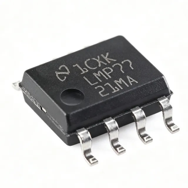
LMP7721MA/NOPB-Q1 - 3fA Input Bias Precision Op Amp | Texas Instruments
The LMP7721MA/NOPB is a single-channel precision operational amplifier from Texas Instruments featuring the industry's lowest guaranteed input bias current of 3 fA (typical), with a specified limit of plus/minus 20 fA at 25C and plus/minus 900 fA at 85C. It operates from a single 1.8V to 5.5V supply, delivers 17 MHz gain-bandwidth product, and 12.8 V/us slew rate in an 8-pin SOIC package. An operational amplifier (op amp) is a high-gain voltage amplifier with differential inputs, forming the foundation of analog signal conditioning within the amplifier IC hierarchy: operational amplifier -> precision amplifier -> analog front end -> signal chain IC. Precision amplifiers are distinguished by near-zero DC error terms - input bias current, offset voltage, and drift. The LMP7721 achieves its femtoampere-class input bias current through patent-pending input bias current cancellation circuitry, which maintains ultra-low bias current over temperature. Critically, the 8-pin SOIC uses a special pinout that isolates the amplifier inputs from the power supply and output pins. With proper board layout techniques, this unique pinout prevents PCB leakage current from reaching the input pins - a decisive advantage over conventional op amp pinouts when guarding is required. As a rail-to-rail input and output amplifier, it maximizes dynamic range in low-voltage systems while drawing low supply current, suiting battery-operated instruments. The wide supply range and high GBW allow use with electrochemical cells, photodiodes, and high-impedance sensors where even picoampere loading corrupts measurements. Typical applications include ionization chamber and electrochemical sensor front ends, photodiode transimpedance amplifiers for low-light detection, pH and dissolved-gas probe buffers, and picoammeter instrumentation. Design tip: to fully exploit the 3 fA bias current, use guard rings connected to the input-following low-impedance node and clean the PCB after assembly - flux residue and moisture can leak picoamperes that dwarf the amplifier's own bias current.
LMP8350MA/NOPB - Ultra-Low Distortion ADC Driver | Texas Instruments
The Texas Instruments LMP8350MA/NOPB is an ultra-low-distortion fully-differential precision ADC driver designed for driving high-performance analog-to-digital converters in data acquisition systems. It ships in an 8-pin SOIC (D, 3.90 mm width) package with an operating temperature range of -40C to +85C and a RoHS-compliant lead-free finish. A fully-differential ADC driver is a special-purpose amplifier that converts a single-ended or differential input into a balanced differential output optimized for the differential input stage of precision ADCs. Within the signal-chain hierarchy (ADC driver -> amplifier -> analog front end -> signal chain), it provides output common-mode control, rejects even-order harmonics, and improves common-mode noise immunity ahead of the converter. Key features include ultra-low distortion across a fully-differential signal path and three selectable operating modes controlled by a unique mode enable pin. As part of TI's PowerWise family, the high power mode is optimized for highest AC dynamic performance, while lower modes trade dynamic range for reduced power consumption - a flexibility few fixed-power differential drivers offer. The /NOPB suffix denotes a no-pull BOM with lead-free, RoHS-compliant plating suitable for global commercial and industrial builds. Technically, the differential architecture inherently cancels common-mode noise and suppresses even-order distortion, which directly benefits THD and SNR when interfacing to precision SAR and delta-sigma converters. The three-mode design lets one footprint serve both battery-powered low-power data acquisition and high-AC-performance instrumentation, differentiating the LMP8350 from conventional fixed-bias fully-differential amplifiers. Typical applications include high-speed precision data acquisition, industrial process control and PLC analog input modules, medical ultrasound front ends, communications receivers and software-defined radios, automated test equipment, and portable battery-powered instruments. Design tip: realize the datasheet ultra-low-distortion performance only with a clean, symmetrical differential PCB layout, tight supply decoupling, and correct MODE pin configuration; verify pricing as of 2026-08-30 with current distributor stock at DigiKey and Mouser.

LMP8350MA/NOPB-Q1 - Ultra-Low Distortion ADC Driver | TI
The Texas Instruments LMP8350MA/NOPB-Q1 is an ultra-low distortion fully-differential precision amplifier designed for driving high-performance analog-to-digital converters (ADCs). Packaged in an 8-pin SOIC (3.90 mm width), it belongs to TI's LMP precision amplifier family and the PowerWise product line, with an operating temperature range of -40C to +85C. Note: the verified web data covers the base LMP8350MA/NOPB; the -Q1 suffix variant should be confirmed against TI ordering information. A fully-differential amplifier (FDA) is a special-purpose amplifier that processes and outputs a differential signal, converting single-ended inputs to differential outputs with excellent common-mode rejection. FDAs are the preferred interface between single-ended analog sources and differential-input ADCs because they cancel common-mode noise, improve dynamic range, and maintain balance in the signal chain. The defining feature of the LMP8350 is its unique mode-enable pin, which lets the designer choose among three operating modes that trade power consumption for dynamic performance. The high-power mode is optimized for the highest AC performance and ultra-low distortion, while lower-power modes save current in battery-powered or thermally constrained systems. As an ADC driver for data acquisition, it achieves very low harmonic distortion suitable for driving precision and high-speed converters. According to the TI datasheet (LMP8350, 36-page document), the device is engineered for driving high-performance precision ADCs in data acquisition systems. Its differential architecture, selectable power modes, and precision DC performance make it a strong fit where signal integrity is paramount. Typical applications include precision data acquisition front ends, industrial process control, test and measurement instrumentation, and medical imaging signal chains - anywhere a single-ended or differential source must drive a differential ADC input without degrading THD or SNR. Design tip: the selected power mode affects both bandwidth and distortion, so verify THD at your target frequency and gain in the chosen mode, and keep the mode pin driven from a defined logic level for deterministic startup.

LMP8640MK-H - 42V Current Sense Amp, 950kHz | Texas Instruments
The Texas Instruments LMP8640MK-H is a precision high-voltage current sense amplifier that detects small differential voltages across an external shunt resistor in the presence of high input common-mode voltages up to 42V, housed in a 6-pin SOT-23-THIN (TSOT-23-6, MK package). The device operates from a 2.7V to 12V supply and accepts common-mode inputs from -2V to 42V, with a unity-gain bandwidth of 950kHz and a slew rate of 1.8 V/us, enabling fast transient response in switching power-supply feedback loops. A current sense amplifier is a specialized analog IC that converts a small differential voltage developed across a low-value shunt resistor into a ground-referenced output proportional to load current. These devices sit in the signal-chain hierarchy between the power stage (MOSFET/IGBT switches) and the control stage (MCU/DSP/ADC), allowing tight closed-loop monitoring of motor, solenoid, and battery currents in industrial, automotive, and telecom systems. Compared with discrete op-amp current-sense solutions, integrated parts like the LMP8640 offer calibrated fixed gains, factory-trimmed offsets, and built-in EMI/RFI filtering that would otherwise consume board area and design effort. Key specifications include a fixed gain of 20 (the -H variant), input offset voltage in the sub-millivolt range, integrated EMI rejection on the input pins, and a low quiescent supply current suited to always-on monitoring. The TSOT-23-6 package provides a small 2.9 mm x 1.6 mm footprint suitable for high-density power-conversion PCBs. The wide -2V to 42V common-mode window makes the part tolerant of load-dump transients in 12V/24V automotive and industrial buses. The architecture uses a precision front-end differential pair followed by gain and output stages optimized for unidirectional or bidirectional current monitoring depending on the reference pin connection. The high 1.8 V/us slew rate preserves signal fidelity during rapid di/dt events such as inrush, PWM switching, and motor commutation. Integrated RFI filtering suppresses the high-frequency noise that would otherwise be rectified by the input stage and appear as DC error at the output. Typical applications include solenoid and valve current monitoring, motor-control phase current sensing, battery-pack charge/discurrent monitoring, 48V telecom rail current telemetry, and high-side current sensing in switching power supplies. The 42V common-mode range covers 12V/24V industrial buses with substantial transient headroom. When designing with this device, place the sense resistor close to the IC input pins and use a Kelvin connection to minimize parasitic resistance errors. The reference pin (REF) sets the output zero-current voltage; for unidirectional sensing tie REF to ground, for bidirectional sensing tie to mid-rail. Decouple VCC with a 100 nF ceramic capacitor placed within 5 mm of the supply pin. This page synthesizes distributor pricing, drop-in pin-compatible alternatives, and application-specific design guidance not consolidated on the manufacturer product page.
LMP8640MK-H/NOPB - 42V Precision Current Sense Amplifier | TI
The Texas Instruments LMP8640MK-H/NOPB is a precision high-voltage current sense amplifier that detects small differential voltages across an external sense resistor in the presence of large common-mode voltages. Housed in a 6-pin SOT-23-THIN (TSOT-23-6, DDC) package, it operates from a 2.7V to 12V supply and accepts common-mode input voltages from -2V to +42V, making it ideal for high-side and low-side current monitoring in 12V, 24V, and 36V industrial buses. A current sense amplifier is an analog IC that amplifies the small differential voltage developed across a shunt resistor carrying the load current, while rejecting the large common-mode voltage present at the resistor terminals. This category sits within the broader hierarchy of operational amplifiers (op-amps) and instrumentation amplifiers, which in turn belong to the signal-conditioning family of analog ICs used in power management, motor control, and battery monitoring. The LMP8640MK-H/NOPB provides fixed internal gain (the "-H" variant specifies the gain version), eliminating the need for external gain-setting resistors and simplifying PCB layout. Key features include a -2V to +42V common-mode input range that survives load-dump transients in automotive and industrial systems, a fixed gain that improves noise immunity versus discrete op-amp solutions, and a 950 kHz gain-bandwidth product that supports fast transient response for current-mode control loops. The device also delivers 1.8 V/us slew rate, low offset, and integrated EMI filtering. The TSOT-23-6 package offers a compact 2.9 mm x 1.6 mm footprint with thermal performance suitable for industrial temperature ranges (-40C to +125C). The LMP8640MK-H/NOPB uses a precision chopper-stabilized input stage and thin-film resistor network to achieve low offset and high common-mode rejection ratio (CMRR). Its high PSRR ensures accurate current measurement even when the supply rail is noisy, which is critical in switched-mode power supply (SMPS) and motor-drive applications where large dv/dt events couple into the measurement node. Typical applications include high-side current sensing in telecom brick modules, battery-pack current monitoring in e-mobility and UPS systems, motor phase-current sensing in industrial drives, and precision load monitoring in solar inverters. The wide common-mode range also suits 48V telecom rails and 24V industrial automation backplanes. When designing with the LMP8640MK-H/NOPB, select a low-inductance Kelvin-connected sense resistor to avoid errors from PCB trace resistance, and place a 0.1 uF supply bypass capacitor as close to the IC as possible. The internal fixed gain eliminates gain-error calculations but the designer must still budget for sense-resistor tolerance and thermal drift. This page synthesizes distributor pricing, drop-in alternatives, and practical design notes not found in the manufacturer datasheet.
LMR321G-GTR - Low-Power Ground-Sense Op Amp | ROHM
The ROHM LMR321G-GTR is a single-circuit, low-power, ground-sense general-purpose operational amplifier in a 5-pin SSOP package. It belongs to the LMR321, LMR358, and LMR324 family of low-voltage operational amplifiers designed for output full-swing operation. The device is intended for portable, industrial, instrumentation, sensor-interface, and low-voltage signal-conditioning applications where low supply-current consumption and operation from low supply voltages are important. An operational amplifier is an analog signal-processing IC that compares two input voltages and drives its output toward a level representing their difference. In a standard amplifier configuration, the feedback network determines the closed-loop gain, while the op-amp supplies high open-loop gain and signal amplification. The ground-sense configuration is particularly useful when the input signal is referenced to ground and the output must remain close to the ground rail. The LMR321G-GTR provides a single amplifier per package, simplifying designs that require only one active device. ROHM describes the LMR321G as a low-voltage, low-power general-purpose operational amplifier with full-swing output. These characteristics make it suitable for battery-powered equipment, current-sense conditioning, sensor interfaces, and low-voltage control systems. The single-channel configuration reduces package count when additional amplifier channels are not required. Its 5-SSOP format also supports compact PCB layouts when compared with larger multi-channel packages. The LMR321, LMR358, and LMR324 families provide single-, dual-, and quad-channel options in a related low-power product grouping. Engineers can therefore standardize on the LMR family while selecting the channel count that matches the circuit. The GTR ordering code identifies the single LMR321G device in a compact SSOP package with a tape-and-reel production configuration. Exact electrical limits, input/output ranges, current consumption, and stability requirements should be confirmed in the manufacturer datasheet before release to production. Typical uses include amplifying signals from low-voltage sensors, buffering analog inputs, conditioning shunt-monitor signals in portable instruments, and providing general-purpose amplification in embedded systems. The full-swing output capability can simplify signal-chain design when the load and bias conditions are compatible with the device's operating region. In precision measurement paths, input offset voltage, input bias current, noise, common-mode range, and output-drive capability remain the principal selection criteria. For layout, keep the feedback loop compact and connect the bypass capacitor close to the supply pins. Maintain the ground reference required by the amplifier circuit and avoid placing high-current return paths beneath sensitive analog signals. Confirm capacitive-load stability and output-current limits for the intended load. When replacing another five-pin amplifier, verify the package drawing, exposed-pad requirements, pin functions, supply range, common-mode range, and output-swing behavior rather than relying only on the package name. This product page combines the manufacturer's device identity with distributor listings, package information, application guidance, comparison fields, and practical design notes. It is intended to accelerate component selection and PCB planning while keeping the final engineering decision tied to the official LMR321G datasheet.

LMR324F-GE2 - 4-Channel Low-Power Op Amp | ROHM
The ROHM Semiconductor LMR324F-GE2 is a four-circuit, general-purpose operational amplifier with rail-to-rail output, low-power operation, and ground-sense capability in a 14-SOP package. It combines four independent amplifiers in one package for compact analog signal-conditioning designs. An operational amplifier, commonly called an op amp, is an active analog component that uses high gain and negative feedback to amplify the voltage difference between its two inputs. The LMR324 belongs to the low-dropout linear-amplifier hierarchy and the broader operational-amplifier semiconductor category. Its ground-sense architecture is intended for applications operating near the lower supply rail, while the full-swing output extends usable output range toward both supply limits. The primary features include four amplifier circuits per package, rail-to-rail output, low supply-current consumption, low-voltage operation, and a general-purpose signal path. These characteristics make the device useful where several low-level signals must be amplified, buffered, or conditioned without allocating a separate package to every channel. The quad configuration can also reduce board area and simplify power distribution compared with four discrete single amplifiers. Each channel is intended for conventional closed-loop operation with external feedback. The ground-sense input arrangement is especially relevant to portable measurement, sensor-interface, and low-voltage control circuits where signals may occupy the lower portion of the supply range. Because final offset, bandwidth, slew rate, common-mode range, and output-current limits determine practical performance, designers should consult the ROHM LMR324F datasheet before setting gain, loading, or bypassing values. Typical uses include low-voltage sensor conditioning, portable instrumentation, industrial control interfaces, battery-powered monitoring, and general-purpose audio or control-signal amplification. A four-channel implementation can provide independent amplification for bridge sensors, analog filters, level conversions within an analog domain, or small actuator-control loops. The same package can also implement repeated circuit blocks where matching and identical part characteristics simplify design review and maintenance. For a new design, pay particular attention to input common-mode range, output swing under load, stability with the selected feedback network, and decoupling requirements. Place supply bypass capacitors close to the device and route each ground reference carefully, especially when all four channels process signals from different sources. Confirm that the electrical limits support the intended supply voltage, source impedance, capacitive load, and ambient temperature. This product page combines the manufacturer product information, package identification, cross-reference findings, and practical engineering guidance. It helps engineers compare the LMR324F-GE2 with its documented alternatives while focusing on fit-for-purpose decisions rather than treating package similarity alone as proof of electrical equivalence.
LMR341G-GTR - 2MHz Low-Power Ground-Sense Op Amp | ROHM
The ROHM Semiconductor LMR341G-GTR is a single CMOS operational amplifier designed for low-voltage, low-power ground-sense applications. It operates from 2.7 V to 5.5 V, provides a 2 MHz gain-bandwidth product and 1 V/µs slew rate, and is supplied in a 6-pin SSOP package. Its low 80 µA supply current, MOSFET input stage, shutdown function, and full-swing output make it suitable for battery-powered sensor and signal-conditioning systems. A ground-sense operational amplifier is a rail-to-rail-input-and-output amplifier optimized for measuring small voltages relative to ground. In the broader component hierarchy, it belongs to the operational-amplifier family, then to amplifier ICs and analog semiconductors. Its low-noise CMOS input stage provides low input bias current, while the full-swing output allows the amplifier to operate close to the positive or negative supply limits without requiring a separate output-bias arrangement. The LMR341G combines a 2 MHz gain-bandwidth product with a 1 V/µs slew rate in a low 2.7 V to 5.5 V supply range. Typical supply current is 80 µA, reducing power consumption in continuously powered equipment. The shutdown function provides a controlled low-power operating state, while the low-bias MOSFET input stage helps minimize source-current loading on high-impedance sensors. These characteristics are particularly useful when sensing battery voltage, resistive sensor outputs, or low-level analog signals. The amplifier is designed for general-purpose low-voltage analog signal conditioning. Its CMOS input stage supports low input bias current, and its output can swing fully across the supply range for improved measurement utilization. A 2 MHz bandwidth is adequate for sensor signals that do not require high-frequency signal processing, while the 1 V/µs slew rate allows the output to track moderate input steps without requiring a larger, higher-power package. Typical uses include battery monitoring, portable instrumentation, sensor-interface circuits, industrial control modules, and low-voltage data-acquisition systems. In a battery-powered design, the shutdown pin can reduce consumption when the measurement function is not required. For high-impedance sensor nodes, the low input bias current helps avoid input-voltage errors caused by leakage through source impedances. PCB implementation should keep the input and feedback components close to their corresponding pins, and the decoupling capacitor should be placed directly between the supply and ground pins. Because ground-sense accuracy depends on the reference plane, connect the sensor return and amplifier ground using a low-impedance layout. Avoid long input traces and unnecessary copper around high-impedance input nodes to reduce leakage and susceptibility to interference. This page combines the manufacturer’s device description, distributor identification, electrical characteristics, package information, sourcing guidance, and practical design considerations. It also identifies family-level drop-in candidates while clearly separating confirmed functions from parameters that require final datasheet and qualification review before a design is released to production.
LMR342F-GE2 - Low-Power Rail-to-Rail CMOS Op Amp | ROHM
The ROHM LMR342F-GE2 is a low-supply-current CMOS operational amplifier intended for ground-sense signal conditioning, with a two-circuit configuration and an 8-SOP package. The LMR342F series is designed around low operating supply voltage, low supply current, low input bias current, input ground sensing, and full-swing output capability. These characteristics make it suitable for battery-powered equipment, sensor amplifiers, battery-monitoring circuits, and voice audio preamplifiers. The product is identified as a rail-to-Rail CMOS amplifier by ROHM and distributor product listings. A CMOS operational amplifier is a voltage-input, voltage-output amplifier whose internal devices consume very little bias current compared with conventional bipolar input stages. In the signal-chain hierarchy, the LMR342F-GE2 belongs to the operational amplifier family within analog and linear integrated circuits, where low input bias current helps preserve the integrity of high-impedance sensor signals. Its ground-sense architecture is particularly relevant when the input signal is referenced close to ground and the amplifier must support low-voltage operation. The key engineering benefits are low operating supply current, low input bias current, ground-sense inputs, and full-swing output behavior. The two-circuit configuration allows two independent amplifier channels in one package, reducing board area where a dual amplifier is required. The low-power operating characteristics also help conserve energy in portable systems, while the rail-to-Rail output can improve usable signal range in low-voltage designs. The manufacturer product page identifies sensor amplification, battery-powered electronic equipment, battery monitoring, and audio preamplification as representative use cases. The LMR342F family is implemented as a CMOS operational amplifier for precision and low-power signal conditioning. The exact electrical limits for the LMR342F-GE2, including supply range, gain-bandwidth product, input offset voltage, input bias current, output swing, and temperature limits, are not fully reproduced in the product excerpts available for this page. Use the manufacturer datasheet for the complete electrical characteristics, test conditions, recommended operating conditions, and pin-description table before finalizing a circuit. Typical designs include current-sense and battery-monitor front ends, low-voltage sensor signal conditioning, portable audio preamplification, and grounded sensor inputs. Because the amplifier is intended for low-voltage and low-power systems, check supply headroom and output swing against the required signal range. The ground-sense input arrangement can simplify sensing relative to ground, while the full-swing output helps maximize usable output range. For PCB implementation, place the device close to the protected sensor node and keep the input path short to minimize leakage and contamination sensitivity. Confirm bypass-capacitor requirements and stability guidance in the manufacturer datasheet. Decouple the supply rail locally and keep high-current return paths away from the input reference to reduce ground-induced errors. This product page combines manufacturer and distributor information with application guidance, selection criteria, package details, and verified drop-in alternatives. It is intended to accelerate engineering evaluation while directing final electrical, thermal, and qualification decisions to the applicable ROHM documentation.
LMR344F-GE2 - Low-Power Quad CMOS Op Amp | ROHM
ROHM Semiconductor LMR344F-GE2 is a low-power, four-circuit CMOS operational amplifier with rail-to-rail input and output operation, optimized for 2.7 V to 5.5 V operation in a 14-pin SOP package. It combines low supply current, low input bias current, input ground sensing, and full-swing output capability for portable and low-voltage analog systems. A CMOS operational amplifier is a voltage-gain device used to amplify weak sensor, audio, or feedback signals while operating from a low-voltage supply. The LMR344F belongs to the operational-amplifier hierarchy, where it provides input-ground sensing and rail-to-rail signal handling for battery-powered equipment, monitoring circuits, and voice audio preamplifiers. Rail-to-rail operation helps preserve usable input and output range when the supply voltage is restricted. The LMR344F family is designed for low operating supply voltage, low supply current, and low input bias current. Its four amplifiers share a common 14-pin SOP package, reducing board area in designs that require multiple signal-conditioning channels. The input-ground-sensing architecture is especially useful when an input signal is referenced to ground rather than to the midpoint of the supply rails. Full-swing output operation allows the amplifier outputs to approach the available supply-rail limits under suitable load conditions. This behavior is valuable in low-voltage systems where signal headroom is limited. The exact bandwidth, slew rate, input offset, noise, and output-current limits should be confirmed against the manufacturer datasheet before defining the closed-loop gain, load, and stability target of a new design. Typical applications include current sensing, portable instrumentation, battery monitoring, sensor signal conditioning, and voice audio preamplification. Multiple amplifiers in one package can support gain stages, differential front ends, filters, output drivers, or active feedback networks when their individual input, output, common-mode, and stability requirements match. For PCB implementation, use the manufacturer pin-description table to assign inputs, outputs, supply rails, and any unused amplifier channels. Keep input and feedback routing short, connect decoupling capacitors close to the supply pins, and provide stable feedback around each amplifier. Verify operation across the complete supply range and load range rather than assuming rail-to-rail input and output alone guarantees usable bandwidth. This product page combines the manufacturer product information with practical device classification, application guidance, design notes, and a same-package alternative assessment. It is intended to help engineers identify the correct amplifier function, validate package compatibility, and plan a robust low-voltage analog implementation.
LMR358F-GE2 - Dual Ground-Sense Op Amp | ROHM Semiconductor
The ROHM Semiconductor LMR358F-GE2 is a dual, ground-sense operational amplifier designed for low-voltage, low-power signal processing. It provides two amplifier channels with rail-to-rail output characteristics in an 8-pin SOP package. The LMR358F belongs to the LMR series of low-power general-purpose operational amplifiers intended for applications where low supply-current consumption, low-voltage operation, accurate sensing near ground, and full-swing output capability are important. An operational amplifier is an analog integrated circuit that compares an inverting input with a non-inverting input and amplifies the voltage difference between them. A ground-sense amplifier is designed to maintain useful input and output behavior near the lower supply rail, making it suitable for sensor signals, battery-powered systems, and low-voltage instrumentation. Within the broader semiconductor hierarchy, this device is a dual-channel operational amplifier, analog amplifier IC, and low-power voltage-feedback amplifier. The principal features of the LMR358F-GE2 are its dual-channel configuration, low-power operating concept, low-voltage supply capability, ground-sense positioning, rail-to-rail output, and ability to swing the output close to the supply rails. The 8-SOP package provides a compact surface-mount footprint for two independent amplifier channels. Its general-purpose positioning also makes it suitable for buffering, amplification, voltage comparison, and signal-conditioning functions rather than limiting it to one specialized measurement topology. The LMR358F family shares its operating concept with the single-channel LMR321 and the quad-channel LMR324. This family relationship provides a practical path for common amplifier functions across different channel counts. The two-channel LMR358F is appropriate when a board requires two amplifiers but does not need the four channels of a quad device. Its full-swing output behavior can simplify interface design when the available output headroom is limited by a low supply voltage. Typical applications include battery-powered sensor conditioning, portable measurement systems, low-voltage industrial interfaces, current-sense amplifiers, general-purpose buffers, and embedded control analog sections. The device can amplify sensor outputs close to ground while operating from a constrained supply, making it particularly useful when the signal of interest occupies only a small portion of the available supply range. It can also be used where two independent analog channels provide a simpler layout than duplicating discrete amplifiers. When designing around the LMR358F-GE2, verify the input common-mode range, output swing, supply voltage, input bias current, noise, offset voltage, and stability requirements against the manufacturer datasheet for the selected operating conditions. Place input and output components close to the relevant device pins, maintain the recommended bypass capacitance, and route feedback paths away from noisy or high-impedance input nodes. Confirm the exposed or exposed-pad details only if the exact mechanical drawing indicates an exposed pad. This product page combines the manufacturer classification, package and channel details, commercial sourcing path, and engineering guidance with a conservative drop-in replacement assessment. It distinguishes a verified same-footprint family alternative from broader LM358-type devices whose package, pin arrangement, or electrical ratings may not support a true drop-in replacement.