Amplifier ICs
بەرهەمەکان (3,200+)

LMR821G-GTR - Low-Power Ground-Sense Op Amp | ROHM
The ROHM Semiconductor LMR821G-GTR is a single-circuit, low-power ground-sense operational amplifier designed for low-voltage and low-supply-current operation. It is packaged in a compact 5-SSOP enclosure, also identified as SC-74A or SOT-753, for space-constrained sensing and signal-conditioning circuits. An operational amplifier is an analog integrated circuit that amplifies the voltage difference between its differential inputs. A ground-sense amplifier is used where the measured signal is referenced close to ground, such as in current-shunt monitoring, low-side sensing, and portable instrumentation. This amplifier belongs to the broader operational amplifier, analog IC, and semiconductor hierarchies. The LMR821G-GTR is specifically identified by ROHM as a low-power ground-sense operational amplifier. Its single-amplifier configuration reduces board area and is suitable for designs that need one sensing channel rather than a dual or quad device. The low-voltage and low-supply-current positioning makes it relevant to compact, battery-powered, and low-energy measurement systems. The LMR821G product family emphasizes low-voltage operation and low supply current. These characteristics help reduce the energy required when the amplifier remains connected to a low-capacity power source. Exact input-voltage limits, output-current capability, offset voltage, noise, bandwidth, and open-loop gain should be taken from the ROHM LMR821G datasheet when setting circuit operating points. Typical uses include low-side current detection, portable sensor interfaces, battery monitoring, and low-voltage signal conditioning. In these applications, the amplifier boosts a small ground-referenced differential signal while adding only modest circuit overhead. Its 5-pin surface-mount package also supports compact layouts, although pad geometry and exposed thermal-pad details must be confirmed against the package drawing. Use the manufacturer pin-description table when assigning PCB tracks because the complete numbered pin list is not included in the product-page summary. Confirm input common-mode range, output swing, unity-gain stability, and recommended external components before finalizing a high-gain or precision design. This page combines the manufacturer product information, exact-MPN distributor records, package details, application guidance, and engineering selection notes in one searchable reference. It is intended to accelerate sourcing and initial circuit assessment, while final qualification should follow the complete ROHM datasheet and application circuits.

LMR822F-GE2 - Dual 5.5MHz RRO Op Amp | ROHM Semiconductor
ROHM Semiconductor LMR822F-GE2 is a dual, rail-to-rail output operational amplifier designed for low-voltage operation from 2.5 V to 5.5 V, with a gain-bandwidth product of 5.5 MHz and a slew rate of 2 V/us. The device is packaged in an 8-SOP and combines two amplifier channels in one package. Its rail-to-rail output, full-swing operating characteristics, low supply-current consumption, high voltage gain, and high slew rate make it suitable for compact analog signal chains. An operational amplifier is a voltage-feedback amplifier used to amplify, buffer, filter, or control analog signals. The LMR822F belongs to the general-purpose operational-amplifier family within analog ICs and the broader signal-conditioning hierarchy. In portable battery-powered equipment, a low-voltage dual amplifier can process two signals or implement a differential stage while reducing package count and board area compared with two single amplifiers. The LMR822F's 5.5 MHz gain-bandwidth product supports closed-loop operation at moderate signal frequencies, while its 2 V/us slew rate improves large-signal response. Rail-to-rail output operation allows the output to approach the available supply rails more closely than a conventional fixed-output amplifier, which is useful when signal headroom is limited. Low supply-current consumption further supports mobile and other battery-powered applications. The dual-channel architecture provides two amplifiers in one 8-SOP package. Each channel can be configured as an inverting amplifier, non-inverting amplifier, voltage follower, comparator-like interface, or active-filter stage, subject to the stability, common-mode, and output-swing limits in the manufacturer datasheet. This flexibility makes the device useful in active filters, sensor interfaces, touch-screen control, audio signal conditioning, and low-voltage industrial systems. Typical applications include portable audio input stages, resistive touch-sensing channels, buffered sensor outputs, active low-pass filters, and low-voltage industrial control boards. The 2.5 V minimum supply supports systems operating from a regulated 3.3 V rail, while the 5.5 V maximum supply accommodates 5 V analog rails. Engineers should confirm frequency, gain, output swing, input range, noise, and stability requirements for the intended configuration. For dependable implementation, keep input and feedback connections short, place compensation or filter components close to the relevant pins, and avoid operating the amplifier beyond its stated 2.5 V to 5.5 V supply range. Verify each channel independently because dual packages share common supply and ground connections. This product page combines the manufacturer's core operating specifications with application guidance, package information, sourcing support, and an engineering comparison of relevant alternatives. It helps designers identify whether the LMR822F-GE2's dual 5.5 MHz architecture is suitable before beginning PCB implementation.

LMR824F-GE2 - Low-Power Rail-to-Rail Op Amp | ROHM
The ROHM Semiconductor LMR824F-GE2 is a low-voltage, low-current, full-swing operational amplifier containing four amplifier circuits in a 14-SOIC package. Each channel supports a 2.5 V to 5.5 V supply range, while the listed per-channel supply current is 26 mA and input bias current is 30 nA. Its rail-to-rail output swing and low-power operating characteristics suit mobile equipment, low-voltage analog systems, active filters, signal conditioning, instrumentation, and audio circuits. An operational amplifier is an analog integrated circuit that amplifies the voltage difference between its inverting and non-inverting inputs. The LMR824F belongs to the broader operational-amplifier and signal-conditioning hierarchy, where four independent channels can implement buffering, gain stages, filters, transducers, and analog signal processing. The quad-amplifier arrangement reduces package count and simplifies common supply routing compared with four separate single-channel devices. The LMR824F family emphasizes low operating supply current, high voltage gain, high slew rate, and output full-swing capability. Its 2.5 V to 5.5 V supply range supports systems operating from a single low-voltage rail. The four-channel configuration is particularly useful when a design requires several matched functional stages, although matching performance between channels should be evaluated from the manufacturer datasheet when precision ratios, offsets, or drift are critical. ROHM describes the LMR824F as a low-voltage, low-current, full-swing operational amplifier with high voltage gain and high slew rate. Its output can approach the supply rails, making it useful in low-voltage circuits where conventional fixed-output amplifiers would leave insufficient signal headroom. Because the four amplifiers share one package, supply bypassing and package-level thermal considerations affect every channel, including channels that are lightly loaded. Typical uses include mobile-equipment signal chains, active analog filters, sensor interfaces, low-voltage audio paths, transducer amplifiers, and general-purpose instrumentation. In a mobile design, the amplifier can buffer sensors or amplify low-level signals while operating directly from a low-voltage rail. In an active-filter implementation, its output swing helps preserve filter amplitude, while the quad format can provide multiple filter or buffer stages with shared supply routing. When laying out the circuit, place the supply-decoupling capacitor close to the positive and ground pins and keep sensitive input traces away from switching nodes and high-current return paths. Confirm the required input common-mode range, output swing, load current, stability, and noise performance for the selected feedback network. The manufacturer datasheet should be used for the exact pin assignment, electrical limits, recommended application circuit, and compensation guidance. This page combines the LMR824F-GE2 product characteristics, commercial sourcing path, package information, application guidance, and design considerations in one engineering-focused reference. It is intended to help designers identify the correct amplifier function, plan a pin-compatible assembly strategy, and evaluate the LMR824F-GE2 for compact low-voltage analog systems.

LMR931G-GTR - 5V Low-Power Rail-to-Rail Op Amp | ROHM
ROHM Semiconductor LMR931G-GTR is a single-channel, low-power operational amplifier characterized by rail-to-rail input and output operation and a 5 V supply. It is supplied in a 5-pin SSOP package with tape-and-reel ordering indicated by the GTR suffix. The device is positioned for compact, low-voltage analog signal-conditioning circuits where low supply current, wide input common-mode range, and full-swing output capability are important. An operational amplifier, or op amp, is an analog integrated circuit that uses high-gain differential amplification to buffer, amplify, or condition signals. The LMR931G belongs to the broader hierarchy of operational amplifier, analog IC, and semiconductor products. Rail-to-rail input operation allows signals to approach the supply rails, while rail-to-rail output operation gives the output stage greater voltage range than a conventional output stage. These characteristics are particularly useful in battery-powered equipment and low-voltage sensor systems where signal headroom is limited. ROHM describes the LMR931G family as a low-power, low-voltage, input/output full-swing operational amplifier. The verified product information identifies a single amplifier with one circuit, a 5 V nominal operating supply, and a 5-SSOP package. The family also includes single, dual, and quad configurations, allowing a system designer to standardize amplifier functions across channels without changing the basic low-power operating approach. Shutdown is specifically identified for the LMR981 and LMR982 family members rather than for the LMR931G. The LMR931G-GTR is suited to low-voltage sensor interfaces, portable measurement systems, signal buffers, audio and communication support circuits, industrial controls, and general-purpose analog amplification. Its low-power operating concept can reduce system burden in applications where the amplifier does not need to operate continuously at high speed. Rail-to-rail input behavior can simplify biasing around midpoint, while full-swing output improves signal utilization at low supply voltages. Designers should verify the electrical limits, common-mode range, output swing, stability requirements, and recommended external components in the ROHM datasheet before release. Decoupling capacitors should be placed close to the supply and ground pins, and feedback and compensation networks should preserve the intended closed-loop response. Input and output behavior must also be checked against source impedance, load impedance, and the operating voltage of the surrounding circuit. This page combines the verified ROHM product information with package, application, comparison, and design guidance focused on practical selection. It identifies the LMR931G-GTR as a low-power, rail-to-rail single op amp and separates confirmed catalog facts from electrical parameters that require confirmation from the manufacturer datasheet.
LMR932F-GE2 - Dual 1.4MHz Low-Power Op Amp | ROHM
The ROHM Semiconductor LMR932F-GE2 is a dual low-power operational amplifier with a 1.4 MHz gain-bandwidth product, a 0.35 V/µs slew rate, and a 1.8 V to 5 V supply-voltage range, housed in an 8-pin SOP package. Its rail-to-rail output and input/output full-swing architecture make it suitable for low-voltage signal conditioning, sensor interfaces, audio paths, and portable equipment. An operational amplifier, or op amp, is a high-gain analog building block that compares two input voltages and drives an output according to their difference. Within the power-management and signal-processing hierarchy, the LMR932F belongs to the operational-amplifier family, where low power consumption, low supply voltage, and rail-to-rail operation make it suitable for battery-powered and portable systems. Two amplifiers are integrated into one package, reducing board area while providing independent channels. The LMR932F-GE2 combines a 1.4 MHz gain-bandwidth product with low power consumption and a typical bias current of 35 nA. Its 0.35 V/µs slew rate supports small- and medium-signal bandwidth applications without requiring a high-speed amplifier. Rail-to-rail output operation helps preserve usable output range near the supply rails, while the 5.5 mV input-offset specification should be considered in precision DC applications. An 8-SOP surface-mount package supports compact, conventional PCB assembly. The ROHM LMR932F series is positioned for low-voltage operation and low supply current. The dual configuration allows common tasks such as sensor amplification, active filtering, buffering, and level shifting to be implemented in one package. Because the amplifier operates down to 1.8 V, it is useful in systems using a single low-voltage rail. Its 1.4 MHz bandwidth makes it more appropriate for general-purpose analog signals than for high-frequency precision instrumentation. Typical uses include portable sensor conditioning, low-voltage audio input stages, industrial control interfaces, battery-powered measurement systems, and general-purpose analog filtering. Two channels are useful when a design needs independent amplification for two sensors, a balanced signal path, or an active filter and buffer combination. The 8-SOP package also simplifies retrofitting and provides a straightforward alternative to larger dual-amplifier packages. Designers should maintain input and output common-mode limits across the full supply range and verify output swing into the intended load. Decoupling capacitors should be placed close to the supply pins, while sensitive input routing should minimize leakage and nearby switching-node coupling. For low-frequency precision work, input bias current, offset voltage, and noise must be evaluated together rather than relying on bandwidth alone. This page organizes the principal electrical and packaging characteristics, practical application guidance, comparison criteria, and sourcing information for engineers evaluating the LMR932F-GE2. It also distinguishes verified same-package replacements from related devices that use different package outlines.
LMR934F-GE2 - Low-Power Quad Rail-to-Rail Op Amp | ROHM
ROHM Semiconductor LMR934F-GE2 is a low-power, four-circuit, input-output full-swing operational amplifier in a 14-SOIC package. The device supports a 5 V supply and is designed for general-purpose applications requiring rail-to-rail output swing. Its quad-channel configuration integrates four amplifiers into one package, reducing board area compared with separate single-channel devices. The LMR934F-GE2 belongs to ROHM's LMR series of low-voltage, low-supply-current operational amplifiers intended for compact and power-conscious analog circuits. An operational amplifier is an active analog building block that compares two input voltages and amplifies their difference. A rail-to-rail output amplifier can approach its supply rails at the output, increasing usable output range in low-voltage systems. The input-output full-swing designation identifies this device as suitable for applications requiring low-voltage operation and broad output range. Within the integrated-circuit hierarchy, the LMR934F-GE2 is an operational amplifier, which belongs to the amplifier IC and analog signal-processing categories. The LMR934F-GE2 provides four amplifier channels in one 14-SOIC package. Its low-power operating approach is suitable for battery-powered and portable equipment where supply efficiency and compactness matter. The rail-to-rail output characteristic supports signal conditioning near the positive and negative limits of a 5 V supply, while the quad configuration can implement filters, buffers, sensor interfaces, or multiple independent gain stages. The manufacturer identifies the LMR934 family as operable with low voltage and low supply current. The integrated four-channel architecture simplifies PCB design by reducing the number of packages and external connections required for multiple amplifier functions. The 14-SOIC footprint supports conventional surface-mount assembly, while full-swing output behavior can improve signal utilization in low-headroom analog systems. Because the device is intended for general-purpose amplification, its suitability for precision instrumentation, audio, or sensor conditioning depends on the complete operating conditions and circuit configuration, including supply voltage, load, bandwidth, and stability requirements. Typical uses include four-channel sensor signal conditioning, low-voltage filtering, buffering, portable test equipment, audio preamplification, and general embedded analog interfaces. In a four-sensor system, all channels can share the same supply and decoupling structure, while independent amplifier sections handle different input signals. In portable equipment, the low-power nature of the LMR series supports compact implementations, although total current consumption depends on the selected device, load condition, operating mode, and external circuitry. Layout should place the supply bypass capacitor close to the device and minimize trace resistance between the capacitor and amplifier supply pins. Keep input and feedback routing short, maintain symmetry between differential inputs, and keep high-impedance input nodes away from switching nodes and digital return currents. Confirm output swing, noise, offset, bias current, stability, and input common-mode range against the manufacturer datasheet before fixing the external feedback network for a particular gain or load. This product page organizes the exact MPN, technical constraints, practical applications, design guidance, and qualified comparison information for engineers evaluating the LMR934F-GE2. It also distinguishes confirmed manufacturer and distributor attributes from parameters that require direct datasheet verification, helping procurement and design teams assess fit without relying on ambiguous family-level descriptions.

LMR981G-GTR - Low-Power Rail-to-Rail Op Amp | ROHM
The ROHM Semiconductor LMR981G-GTR is a single-circuit, low-power operational amplifier with rail-to-rail input and output capability, supplied in a 6-pin SSOP embossed tape-and-reel package. The device is designed for low-voltage systems that require an amplifier to operate close to both supply rails while keeping supply current low. Its general-purpose configuration makes it applicable to sensor buffering, audio signal conditioning, low-voltage filtering, and general analog signal amplification. An operational amplifier, or op amp, is an analog integrated circuit that provides high voltage gain in an open-loop configuration. Rail-to-rail input and output amplifiers can accept input signals close to the negative and positive supply rails and can swing their output close to those rails. This capability is useful in low-voltage systems because it expands the usable input and output range without requiring a separate midrail bias reference. The LMR981G belongs to the ROHM LMR series of low-power input-output full-swing operational amplifiers. According to the manufacturer product page, this series was developed for single, dual, and quad amplifier configurations that operate at low voltage and low supply current. The LMR981G is the single-amplifier configuration, while the LMR982 family adds a shutdown function. Its 5 V supply rating, 6-pin SSOP package, and rail-to-rail input/output architecture make it a compact choice for portable and embedded analog designs. Key electrical characteristics include one amplifier circuit per package, general-purpose signal conditioning, low-power operation, and full-swing input and output behavior. The datasheet defines the detailed input bias current, input offset voltage, unity-gain bandwidth, slew rate, noise specifications, and output-current limits for design calculations. Because this page does not reproduce those numeric ratings, engineers should use the manufacturer datasheet for precision AC and DC design work. Typical applications include conditioning the output of resistive sensors, buffering ADC inputs, implementing active filters, and amplifying low-level analog waveforms from portable instruments. The SSOP-6 package is also useful where board space is restricted, although its small body and limited copper area require attention to thermal rise when the amplifier operates continuously near its output-current limit. When designing around the LMR981G-GTR, confirm the exact input common-mode range, output swing, unity-gain bandwidth, and noise figures for the selected supply voltage. Place the bypass capacitor close to the supply pin, keep feedback resistors close to the amplifier inputs, and avoid driving a capacitive load directly unless the stability behavior has been verified. This page combines the manufacturer product information with a practical selection guide, packaging details, design cautions, and a structured comparison of drop-in candidates. It adds engineering context around the LMR981G-GTR without replacing the manufacturer datasheet for guaranteed limits, test conditions, and absolute maximum ratings.

LMV321IDBVR - 1-MHz RRO Op Amp Single 5.5V | Texas Instruments
The Texas Instruments LMV321IDBVR is a single-channel, low-voltage, rail-to-rail output CMOS operational amplifier in a 5-pin SOT-23 (DBV) package. It operates from a single supply of 2.7 V to 5.5 V (5 V performance characterized), delivers a unity-gain bandwidth of 1 MHz, and offers rail-to-rail output swing from a low 130 µA typical supply current. The part is qualified for -40 °C to +125 °C operation and is offered on 3000-piece tape-and-reel. A rail-to-rail output (RRO) op amp is a linear amplifier whose output voltage can swing to within tens of millivolts of either supply rail, maximizing dynamic range in low-voltage single-supply systems. Compared with general-purpose amplifiers that lose 1 V to 2 V of headroom on each side, an RRO part lets the designer use the full ADC input range on a 3.3 V or 5 V rail. The LMV321 belongs to the broader family of CMOS operational amplifiers, a category of analog ICs that trades the lower noise of bipolar parts for very low quiescent current and single-supply operation. Key features include 1 MHz gain bandwidth product, 130 µA typical quiescent current, no output phase reversal, low crossover distortion, and an industry-standard 5-pin SOT-23 footprint. An internal ESD clamp and EMI filtering are characteristics of the larger LMV321A family; the original LMV321 line is recommended for cost-sensitive designs where these features are not required. The device is unity-gain stable and drives 2 kΩ loads comfortably at 5 V. The LMV321 is built on a CMOS process with a differential input pair and a rail-to-rail class-AB output stage, which keeps crossover distortion low compared to single-ended class-A CMOS outputs. The PSRR is specified at 50 dB at 1 kHz, and the input common-mode range extends from the negative rail to within 1.2 V of the positive rail — adequate for single-supply sensor buffers and instrumentation front-ends. Typical applications include single-supply sensor signal conditioning, current-sensing shunts in portable battery packs, low-side current monitors, headphone line drivers, and 5 V active filters. The part is widely used as a buffer/amplifier stage between photodiodes, thermistors, or strain gauges and downstream ADCs in IoT nodes. When designing with this device, place a 1 nF to 10 nF decoupling capacitor within 2 mm of the VCC pin and keep input trace lengths short to limit leakage-induced offsets. For driving heavy loads or large capacitive loads, add a 50 Ω to 100 Ω series resistor at the output to prevent oscillation. This page synthesizes distributor pricing, drop-in same-footprint alternatives, and practical design notes not found in the manufacturer datasheet.
LMV321ILT - Single Low-Power Op Amp | STMicroelectronics
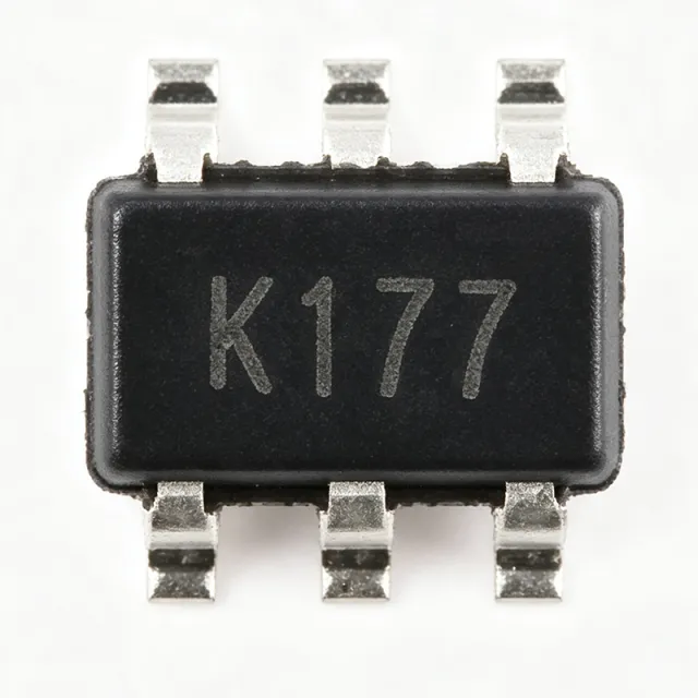
The LMV321ILT is a single, low-power, general-purpose operational amplifier from STMicroelectronics, offered in the compact SOT-23-5 package. It operates from a supply voltage range of 2.7V to 5.5V, making it suitable for battery-powered and portable applications. The device features a typical supply current of 130 µA, a gain-bandwidth product of 1.3 MHz, and an input offset voltage of 1 mV (max). Data verified as of 2026-08-05. An operational amplifier (op-amp) is a high-gain voltage amplifier with differential inputs and a single-ended output. It is a fundamental building block in analog electronics, used in signal conditioning, filtering, and amplification. In the hierarchy of electronic components, an op-amp falls under linear ICs, which are part of the broader category of analog integrated circuits. The LMV321ILT is a low-power variant, optimized for applications where power consumption is critical, such as battery-operated devices. Key features of the LMV321ILT include rail-to-rail input and output stages, which allow the output to swing close to the supply rails, maximizing dynamic range in low-voltage applications. The device also offers a wide operating temperature range of -40°C to +125°C, ensuring reliability in harsh environments. Its low supply current of 130 µA (typical) extends battery life in portable electronics. The LMV321ILT is built on a CMOS process, providing high input impedance and low input bias current. This makes it suitable for interfacing with high-impedance sensors and transducers. The device is unity-gain stable, simplifying design in buffer and follower configurations. Its small SOT-23-5 package is ideal for space-constrained PCB layouts. Typical applications include portable instrumentation, battery-powered signal conditioning, sensor interfaces, and active filters. In portable medical devices, the low power consumption and small footprint are critical. In sensor signal conditioning, the rail-to-rail output ensures maximum signal swing for ADC interfacing. When designing with the LMV321ILT, ensure proper decoupling of the power supply with a 0.1 µF ceramic capacitor placed close to the V+ pin. The input common-mode voltage range includes ground, allowing single-supply operation with ground-referenced inputs. Avoid exceeding the absolute maximum supply voltage of 6V to prevent damage. This page synthesizes distributor pricing, drop-in alternatives, and practical design notes not found in the STMicroelectronics datasheet, providing a comprehensive resource for engineers evaluating the LMV321ILT.
LMV331QDBVRQ1 - AEC-Q100 Single Comparator, Open-Collector, SOT-23-5 | TI
The Texas Instruments LMV331QDBVRQ1 is an automotive-qualified (AEC-Q100) single-channel general-purpose low-voltage analog comparator housed in a 5-pin SOT-23 (DBV) package. It operates from a single 2.7 V to 5.5 V supply, draws a typical quiescent current of 60 µA, and provides a propagation delay of 600 ns with an open-collector output that supports wire-ORed configurations and easy level shifting. What is a comparator? A comparator is an analog integrated circuit that compares two input voltages and drives its output to a logic level indicating which input is larger. The LMV331-Q1 belongs to the analog comparator family within the broader signal-conditioning and power-management hierarchy, occupying the same role in the IC taxonomy as op-amps, references, and timers. Comparators are essential building blocks in voltage monitoring, threshold detection, zero-crossing detectors, and oscillator/waveform-shaping circuits. Key specifications of the LMV331QDBVRQ1 include an input common-mode voltage range that includes ground, low output saturation voltage, push-pull compatible open-collector output stage, and an operating temperature range of -40 °C to +125 °C (automotive Grade 1). The part is offered in the SC-74A / SOT-753 / SOT-23-5 footprint, making it one of the smallest qualified comparators available for space-constrained automotive modules. Internally, the LMV331 uses a PNP input stage and a low-voltage CMOS-compatible architecture that allows operation down to 2.7 V while maintaining a ground-referenced input range. The open-collector output requires an external pull-up resistor, which gives designers the freedom to level-shift the output to a voltage higher than the supply rail (for example, driving a 3.3 V logic output from a 5 V supply comparator) or to combine multiple comparator outputs on a single bus. Typical applications include automotive body controllers, battery management threshold detectors, sensor signal conditioning, window comparators, and oscillator circuits. The wide supply range and low quiescent current also suit portable consumer products, IoT battery-powered nodes, and industrial control systems requiring automotive-grade reliability. When designing with this part, choose the pull-up resistor value to balance switching speed and power dissipation. Avoid placing large capacitive loads directly on the open-collector output; use a small series resistor if capacitive loading cannot be avoided to limit inrush current during saturation-to-release transitions. This page synthesizes distributor pricing, drop-in alternatives, and practical design notes not found in the manufacturer datasheet, helping engineers source and apply the LMV331QDBVRQ1 efficiently.

LMV344IPWR - Quad 1MHz Rail-to-Rail CMOS Op Amp | TI
The Texas Instruments LMV344IPWR is a quad CMOS operational amplifier with rail-to-rail output swing and shutdown capability, packaged in a 14-pin TSSOP (PW). It operates from a single supply of 2.7V to 5.5V (absolute 2.5V to 5.5V range per datasheet) and delivers a gain bandwidth product of 1MHz with a 1V/us slew rate. An operational amplifier (op amp) is a high-gain voltage amplifier with differential inputs and single-ended output, used for amplification, filtering, and signal conditioning. The LMV344IPWR belongs to the CMOS op amp category within the linear amplifier family of analog ICs, a fundamental building block of analog signal processing in the power management and sensor front-end hierarchy. Key features include rail-to-rail output swing, which maximizes dynamic range in low-voltage single-supply systems, and a shutdown mode that reduces supply current for battery-powered designs. A PMOS input stage provides an ultra-low input bias current of 1pA (typical) and 0.25mV typical input offset voltage, making the part suitable for high-impedance sensor interfaces. Despite low quiescent power (100uA per amplifier typical), the device can source/sink up to 75mA output current, unusual for such a low-power op amp. Technically, the CMOS architecture with PMOS input contributes to high input impedance and low bias current, while the rail-to-rail output stage allows output swing close to both supply rails, critical where headroom is limited. The device is specified over the industrial temperature range of -40C to +125C. Typical applications include battery-powered instrumentation, portable medical devices, sensor signal conditioning, and active filters in 3V or 5V systems. AEC-Q100 qualified LMV344QIPWRQ1 extends use to automotive designs. When designing, decouple supply pins with 0.1uF ceramic capacitors placed close to the IC, and tie the shutdown pin to the correct logic level to avoid unintended shutdown. Prices as of 2026-08-30 start near $0.49 at LCSC.
LMV344QIPWRQ1 - Quad 1MHz Rail-to-Rail Op-Amp | TI Automotive
The Texas Instruments LMV344QIPWRQ1 is an automotive-grade (AEC-Q100), quad-channel CMOS operational amplifier delivering 1 MHz gain-bandwidth and 75 mA of high output current from a single 2.7 V to 5.5 V supply, packaged in a 14-pin TSSOP (PW) for surface-mount assembly. An operational amplifier is a high-gain DC-coupled voltage amplifier that, with external feedback networks, performs signal amplification, buffering, filtering, and comparison functions. Within the power-management hierarchy, the LMV344 belongs to the general-purpose low-voltage op-amp family (LMV341/LMV342/LMV344 single/dual/quad), itself a subset of CMOS amplifiers within the broader analog signal-chain category. Key features include rail-to-rail output swing, which maximizes dynamic range on low-voltage 3.3 V and 5 V rails; 75 mA output current capability, roughly 10x a general-purpose op amp, enabling direct driving of low-impedance loads such as ADC inputs, capacitive loads through isolation resistors, and transmission lines; and operation up to 125C ambient, supporting under-hood and body-electronics environments. The quad configuration saves board space and BOM cost versus four single-channel devices. The CMOS input architecture provides low input bias current and low quiescent power, while the rail-to-rail output stage minimizes headroom losses near the supply rails. The -Q1 suffix denotes AEC-Q100 qualification and PPAP support for automotive production, distinguishing it from the commercial LMV344. Typical applications include automotive sensor signal conditioning, battery-current and voltage monitoring front ends, driving ADCs in body-control modules, LED indicator drivers, and audio buffers in instrument clusters. The 75 mA drive also suits speaker or actuator buffer duties at low frequencies. Design tip: with 75 mA drive capability, verify power dissipation in the small TSSOP-14 package when sourcing high current continuously, and add an isolation resistor (10-50 ohm) when driving large capacitive loads to preserve phase margin. Pricing references are as of 2026-08-29.

LMV358IDT - Dual Low-Power Op Amp | STMicroelectronics
The LMV358IDT is a dual low-power operational amplifier from STMicroelectronics, designed for battery-powered and portable applications. It operates from a single supply voltage ranging from 2.7V to 5.5V, with a typical quiescent current of 210 µA per amplifier. The device is offered in the SOIC-8 package, making it suitable for space-constrained designs. Data verified as of 2026-08-05. An operational amplifier (op amp) is a high-gain voltage amplifier with differential inputs and a single-ended output. It is a fundamental building block in analog electronics, used in signal conditioning, filtering, and amplification tasks. The LMV358IDT belongs to the low-power op amp category, which prioritizes minimal power consumption for battery-operated devices. In the hierarchy of analog components, it sits under linear ICs, which are part of the broader integrated circuits family. Key features of the LMV358IDT include a low supply current of 210 µA per channel, a wide supply voltage range of 2.7V to 5.5V, and a rail-to-rail output stage that swings within 10 mV of the supply rails. The input common-mode voltage range extends to ground, allowing single-supply operation. The device also features a gain bandwidth product of 1.3 MHz and a slew rate of 0.45 V/µs, sufficient for audio and sensor signal conditioning. The LMV358IDT uses a bipolar technology with a class-AB output stage, providing low crossover distortion. The input stage is a PNP transistor pair, enabling the input common-mode range to include ground. The output stage can source and sink current, with a short-circuit current of 160 mA. The device is internally frequency compensated for unity-gain stability, simplifying design. Typical applications include battery-powered instrumentation, portable medical devices, sensor signal conditioning, and active filters. The low quiescent current extends battery life, while the rail-to-rail output maximizes dynamic range in single-supply systems. The wide supply range also allows operation from 3.3V or 5V logic rails. When designing with the LMV358IDT, ensure proper decoupling with a 0.1 µF capacitor close to the supply pin. The input common-mode range includes ground, but for best performance, keep inputs within the specified range. The output can drive capacitive loads up to 100 pF without oscillation, but larger loads may require a series resistor. This page synthesizes distributor pricing, drop-in alternatives, and practical design notes not found in the STMicroelectronics datasheet, providing a comprehensive resource for engineers.
LMV358SG-13 - Dual 1MHz Rail-to-Rail Op Amp, 8-SO | Diodes Inc
The Diodes Incorporated LMV358SG-13 is a dual-channel, low-voltage, rail-to-rail output operational amplifier supplied in an 8-pin SOIC package and shipped on 13-inch reel packaging. Per the manufacturer datasheet, the part provides a 1 MHz gain-bandwidth product, a 1 V/µs typical slew rate, and operates from a single 2.7 V to 5.5 V supply, targeting general-purpose and cost-sensitive analog designs. A rail-to-rail output operational amplifier is a type of operational amplifier (OP-Amp) whose output voltage can approach both supply rails, unlike traditional amplifier topologies whose swing is limited to 1.5-2 V below each rail. Within the broader hierarchy, this device belongs to the linear amplifier family, which sits under integrated circuits and power management/analog signal chain categories. Rail-to-rail capability enables designs to maximize dynamic range in low-voltage single-supply systems such as battery-powered portable equipment. Key features include a 1 MHz gain-bandwidth product, 1 V/µs slew rate, low-voltage 2.7 V to 5.5 V single-supply operation, and CMOS input architecture suitable for general-purpose signal conditioning. The LMV321/LMV358/LMV324 family from which this part derives was designed to effectively reduce cost and footprint at low voltage levels, with the SG-13 suffix indicating 8-SOIC package and 13-inch reel quantity. This makes the part especially attractive for high-volume consumer and industrial designs. Internally the device uses CMOS input stages that support low input bias current and a common-mode range that includes the negative rail, while the output stage is designed to swing within millivolts of either rail. Compared with bipolar-input rail-to-rail op amps, the LMV358 family typically delivers lower input bias current at the cost of slightly higher input-referred voltage noise. Typical applications include portable consumer electronics, battery-powered sensor interfaces, signal conditioning for ADC front-ends, general-purpose active filters, headphone driver stages, and transducer pre-amplification. The dual-channel configuration allows space-efficient implementation of difference amplifiers, instrumentation front-ends, or dual-pole Sallen-Key filters. When designing with this part, ensure input common-mode voltage stays within the specified range, place a 0.1 µF decoupling capacitor close to the supply pin, and verify output drive capability against the load. The rail-to-rail output stage requires minimum output current loading to maintain linearity near the rails. This page synthesizes distributor pricing, drop-in alternatives, and practical design notes not found in the manufacturer datasheet, giving a more complete engineering reference for component selection.

LMV761MFX/NOPB - 120ns Precision Comparator w/ Shutdown | TI | SOT-23-6
The Texas Instruments LMV761MFX/NOPB is a single-channel, 120-ns, low-voltage precision comparator with shutdown and a push-pull output stage, housed in a 6-pin SOT-23 (DBV) package. It operates from a 2.7 V to 5 V single supply, draws a typical quiescent current well below 1 mA in active mode, and integrates a SHDN pin that drops supply current to a sub-microampere level when pulled low. The part is specified over the -40C to +125C industrial temperature range and is lead-free / RoHS compliant (NOPB suffix). A comparator is a high-gain differential amplifier whose output swings fully high or fully low depending on which of its two inputs is more positive. Precision comparators such as the LMV761 are distinguished from general-purpose comparators by very low input offset voltage, low input bias current, and tight propagation delay, making them the reference building block for threshold detection, zero-crossing detection, and analog signal conditioning. The LMV761 belongs to the linear / comparator IC category, sits in the signal-chain hierarchy between analog front-ends and digital logic, and is widely used in battery-powered and space-constrained designs. Key features of the LMV761MFX/NOPB include a 120 ns typical propagation delay, push-pull CMOS output (no pull-up resistor required), rail-to-rail input common-mode range, an active-low shutdown pin for power management, internal hysteresis for clean switching on slow signals, and ESD protection on the pins. The push-pull topology drives CMOS/TTL loads directly with symmetric rise/fall times, which is critical when the comparator output feeds a high-impedance logic input or a microcontroller interrupt. Architecturally, the LMV761 uses a bipolar-CMOS input stage that yields low input bias current combined with low offset, followed by a fast latch and CMOS output drivers. The shutdown circuit is implemented as a gated bias path that collapses the input stage current when SHDN is low, while preserving the output in a defined high-impedance state so downstream circuitry can hold the last logic level. Typical applications include battery management (over-voltage / under-voltage detection), threshold detectors in industrial sensor modules, line drivers and zero-crossing detectors for power-line monitoring, alarm and security subsystems, and general signal conditioning ahead of an MCU ADC. Designers favor it for any 3.3 V or 5 V system that needs a fast, low-power, board-space-saving comparator. When designing with this part, place a 0.1 uF bypass capacitor within a few millimeters of VCC, keep input trace lengths short to minimize parasitic feedback that causes oscillation, and ensure the SHDN pin (when unused) is tied high through a resistor, never left floating. The push-pull output cannot be wire-ORed with another comparator output; if that topology is required, select an open-drain variant instead. This page synthesizes distributor pricing, drop-in same-package alternatives, comparison parameters, and practical PCB-level design notes that complement the manufacturer datasheet without replacing it.
LMV841MGX/NOPB - 4.5MHz RRIO CMOS Op-Amp, SC-70-5 | TI
The Texas Instruments LMV841MGX/NOPB is a single-channel CMOS input, rail-to-rail input and output (RRIO), low-power operational amplifier that operates over a wide 2.7 V to 12 V supply range. The device is housed in a space-saving 5-pin SOT-SC70 (DCK) package and offers 4.5 MHz unity-gain bandwidth, low offset voltage, and a CMOS input stage. According to the manufacturer datasheet, the LMV84x family is optimized for high-impedance sensor interfaces and battery-powered applications. A CMOS-input op-amp (operational amplifier) is a linear amplifier whose input stage is built using CMOS transistors rather than bipolar junction transistors. CMOS inputs provide extremely high input impedance (very low bias current), making them ideal for interfacing with high-impedance sensors such as photodiodes, electrochemical cells, and piezoelectric transducers. Rail-to-rail input and output (RRIO) capability allows the input common-mode signal and the output swing to reach within millivolts of both supply rails, maximizing dynamic range when operating from low-voltage supplies. These characteristics position the LMV841 within the broader hierarchy of operational amplifier -> amplifier IC -> analog signal chain -> integrated circuit. Key features include a 4.5 MHz gain-bandwidth product, low input bias current due to the CMOS input stage, rail-to-rail input and output swing, low supply current consumption for battery operation, and operation from 2.7 V to 12 V single supply. The CMOS input stage virtually eliminates input bias current errors that would otherwise limit high-impedance sensor designs, while the RRIO capability preserves dynamic range in low-voltage single-supply systems. The 5-pin SC-70 package measures only 2.0 mm x 1.25 mm, enabling high-density analog front-end designs. Typical applications include battery-powered instrumentation, photodiode transimpedance amplifiers, handheld medical devices, sensor signal conditioning, active filters, and portable audio signal chains. The wide supply range allows direct interfacing to lithium-ion cells (3.6 V nominal, 4.2 V peak) as well as 9 V industrial rails without level shifting. When designing with the LMV841, place a 0.1 uF decoupling capacitor within 5 mm of the supply pin to minimize noise coupling. Avoid placing large resistive loads directly at the output when operating near the rails, as the output drive capability degrades within approximately 50 mV of either rail under heavy loading. This page consolidates distributor stock and pricing data, drop-in alternative part numbers in the same SC-70-5 footprint, and practical SC-70 PCB layout guidance that augments the manufacturer datasheet for accelerated component selection.

LMV932MMX/NOPB - Dual 1.8V RRIO Op Amp 1.5MHz | TI
The Texas Instruments LMV932MMX/NOPB is a dual low-voltage, low-power operational amplifier from the LMV93x-N family, operating from a 1.8V to 5.5V supply with rail-to-rail input and output (RRIO) performance in a space-saving 8-pin VSSOP package. It provides 1.5MHz gain-bandwidth and can source up to 5mA of output current, making it well suited to battery-powered and portable signal conditioning. An operational amplifier (op amp) is a high-gain voltage amplifier with differential inputs and a single-ended output, the fundamental building block of analog signal chains. Within the power-management hierarchy of a system, general-purpose op amps such as this one sit between sensors and ADCs, performing amplification, filtering, buffering, and level shifting. The LMV93x-N family spans a single (LMV931-N), dual (LMV932-N), and quad (LMV934-N) to cover channel-count scaling. Key features include guaranteed operation down to 1.8V for single-cell Li-Ion or two-cell alkaline end-of-life conditions, rail-to-rail input common-mode that extends to both supply rails, and rail-to-rail output swing that maximizes dynamic range at low supply voltages. The NOPB suffix confirms lead-free, RoHS-compliant packaging. Temperature range is -40C to +125C, and the MMX suffix denotes the VSSOP-8 (DGK) surface-mount package suited to area-constrained PCBs. The rail-to-rail input stage typically uses complementary PMOS/NMOS differential pairs to avoid common-mode crossover distortion near the rails, allowing sensor signals at or near ground or VCC to be processed accurately. The output stage swings within millivolts of the rails under light load, maximizing ADC input utilization at 1.8V operation. Typical applications include mobile phone and tablet audio or sensor front ends, battery-powered instrumentation, active filters in portable medical devices, and low-voltage ADC driver stages. The compact VSSOP footprint makes the part a good fit for dense multi-channel boards. Design consideration: at 1.8V supply, output current capability and headroom are limited; keep load impedances above several kilohms and verify bandwidth requirements, since 1.5MHz gain-bandwidth means closed-loop gains of 10 or more restrict usable signal bandwidth to well under 150kHz.

LT1001ACH - ±22V Precision Op Amp, TO-5 | Analog Devices
The Analog Devices LT1001ACH is a single-circuit precision operational amplifier designed for accurate signal conditioning with supply voltages extending to ±22 V. It is packaged in an 8-pin TO-5 hermetic metal package and is identified by Analog Devices as a production part. The combination of precision-op-amp architecture, low-noise operation, and a wide supply-voltage range makes the LT1001ACH suitable for instrumentation, industrial measurement, audio signal paths, and analog systems that must preserve small signals over long signal chains. An operational amplifier is an active analog integrated circuit that amplifies the voltage difference between its inverting and non-inverting inputs. The precision operational-amplifier category extends that basic function with emphasis on low input offset voltage, low input bias current, low noise, high open-loop gain, and stable behavior over temperature and time. Within the broader semiconductor hierarchy, the LT1001ACH belongs to the precision amplifier family, which supports instrumentation, measurement, conversion, and feedback-control systems. The manufacturer describes the LT1001 family as a precision operational amplifier with close attention to the distribution of several key parameters. The LT1001ACH combines a ±22 V maximum supply capability with one amplifier circuit in the TO-5 package. Its precision-oriented design is useful where input offset error can affect measurement accuracy, particularly in high-gain amplifier stages, current-to-voltage converters, low-level sensor interfaces, and precision reference buffers. The LT1001 architecture is intended to provide predictable behavior in real feedback networks. Because this device is a voltage-feedback operational amplifier, external feedback components determine closed-loop gain and bandwidth. Its accuracy is most valuable when operating near the electrical center of the supported supply range, allowing output swing and common-mode range to remain compatible with the signal being amplified. Stable feedback design and careful grounding remain essential to preserve the precision expected from the device. Typical uses include precision instrumentation amplifiers, low-level sensor front ends, laboratory measurement equipment, audio preamplification, active filters, and analog signal-conditioning modules. In a typical application, the amplifier operates in an inverting or non-inverting configuration with external resistors setting the gain and capacitance or filtering components controlling bandwidth. The 8-pin TO-5 package also supports applications where a conventional metal-can amplifier is preferred for mechanical compatibility or historical PCB assemblies. For a new design, verify input bias current, input offset voltage, noise, common-mode range, output swing, slew rate, gain-bandwidth product, and compensation requirements against the Analog Devices LT1001 datasheet. Decoupling capacitors should be placed close to the supply pins, and the circuit should provide adequate output-current margin for the selected load and feedback topology. This product record combines manufacturer documentation, component identification, application guidance, and engineering-oriented replacement analysis. It also distinguishes verified electrical characteristics from parameters requiring circuit-specific confirmation, helping engineers evaluate the LT1001ACH for precision analog designs before committing to a footprint or qualification plan.

LT1001ACP - Precision 0.8 MHz Op Amp in 8-PDIP | Texas Instruments
Texas Instruments LT1001ACP is a precision, general-purpose operational amplifier with one amplifier circuit per package, a maximum input offset voltage of 60 uV, and a gain-bandwidth product of 0.8 MHz. The device is supplied in an 8-pin PDIP package for through-hole PCB installation. An operational amplifier, or op amp, is a high-gain differential amplifier that uses external feedback to set its closed-loop behavior. The LT1001 belongs to the broader hierarchy of linear amplifier, analog IC, and semiconductor devices. Its low offset specification makes it useful when the difference between two input voltages must be measured or amplified accurately, while its 0.8 MHz bandwidth supports moderate-frequency signal paths rather than high-speed applications. The principal features of the LT1001ACP include a 60 uV maximum input offset voltage, a 0.8 MHz gain-bandwidth product, one amplifier per package, and an 8-pin PDIP package. The through-hole package provides generous pin spacing and mechanical robustness for prototypes, educational systems, laboratory equipment, and selected production boards that are not constrained to surface-mount assembly. The LT1001 uses precision bipolar operational-amplifier circuitry. Its offset-trim terminals support factory or user-level offset adjustment, while the amplifier provides the differential input and feedback connections required for inverting, non-inverting, summing, filtering, and instrumentation configurations. Exact input bias current, slew rate, supply-current, common-mode range, output swing, and temperature limits are not stated on the accessible manufacturer product listing and should be confirmed against the LT1001 manufacturer data sheet before final circuit sign-off. Typical uses include low-level signal conditioning, bridge and transducer front ends, precision current-loop interfaces, laboratory instrumentation, audio and control circuits, sensor amplification, and active filtering. The 0.8 MHz bandwidth makes it appropriate for signal bandwidths below that limit when slew-rate and gain requirements are also acceptable. When designing a board around the LT1001ACP, check the 8-pin PDIP pinout and leave adequate clearance around the package for conventional DIP sockets or leaded soldering. Keep feedback resistors and sensitive input traces away from switching nodes, provide local supply bypassing, and verify the required output swing at the selected supply voltage before committing the schematic. This product page combines manufacturer specifications, package information, sourcing guidance, verified alternatives, and practical design notes to support component selection and PCB planning for the LT1001ACP.
LT1001CD - Precision Op-Amp 8-SOIC | Texas Instruments
The Texas Instruments LT1001CD is a precision operational amplifier with industry-leading DC accuracy, supplied in an 8-pin SOIC (D) package. It features a maximum input offset voltage of 110 uV, a unity-gain bandwidth of 0.8 MHz, and a low offset voltage drift of 0.3 uV/C. The single-channel amplifier is built for instrumentation, precision signal conditioning, and industrial measurement front ends. A precision op-amp is a type of operational amplifier designed to minimize the input-referred errors (offset voltage, bias current, drift, and noise) that limit DC accuracy. In the system hierarchy, the LT1001CD sits at the precision tier of general-purpose amplifiers, above standard 741-class parts and below chopper-stabilized zero-drift amplifiers. It is the workhorse of 16-bit and lower data-acquisition front ends, weigh scales, strain-gauge bridges, and thermocouple conditioning circuits where 10-100 uV of error must be resolved over industrial temperature ranges. Key features of the LT1001CD include 110 uV maximum input offset voltage, 4 nA maximum input bias current, 102 dB minimum open-loop gain, and 0.3 uV/C offset voltage drift. The device operates from +/-3 V to +/-18 V dual supplies or 6 V to 36 V single supply. Its bipolar input stage supports true differential sensing across the full input common-mode range, including ground-referenced signals when operated from a single supply. The C-grade commercial temperature range is 0C to +70C. Architecturally, the LT1001CD uses a precision bipolar input stage with active bias compensation, allowing it to maintain low offset and bias current over temperature without chopper-induced switching artifacts. The internal compensation network is unity-gain stable, eliminating the need for external compensation capacitors. The result is a versatile amplifier that combines 741-class simplicity with significantly tighter DC specifications. Typical applications include precision weighing scales, strain-gauge and load-cell amplifiers, thermocouple and RTD signal conditioning, medical instrumentation front ends, 16-bit SAR ADC input buffers, industrial process-control analog inputs, and reference-voltage buffering for precision DACs. The 8-SOIC package is footprint-compatible with industry-standard dual op-amps, simplifying board reuse in legacy designs. When designing with the LT1001CD, take care to provide adequate supply decoupling (100 nF ceramic close to each supply pin) and route sensitive bias-current paths to avoid leakage. Optional pins 1 and 8 support external offset nulling via a 10 kOhm potentiometer; if unused, leave them open. The input common-mode range extends to the negative supply, making true ground sensing possible on a single rail. This page synthesizes distributor pricing, drop-in alternatives, and practical design notes not found in the manufacturer datasheet alone. The information is anchored to the official Analog Devices LT1001 datasheet and cross-checked against Rochester Electronics, DigiKey, and JAK Electronics stock data as of 2026-10-22.
LT1001CDR - Precision Op-Amp 8-SOIC | Texas Instruments (Tape & Reel)
The Texas Instruments LT1001CDR is a precision operational amplifier with industry-leading DC accuracy, supplied in an 8-pin SOIC (D) package. It features a maximum input offset voltage of 110 uV, a unity-gain bandwidth of 0.8 MHz, and a low offset voltage drift of 0.3 uV/C. The single-channel amplifier is built for instrumentation, precision signal conditioning, and industrial measurement front ends. A precision op-amp is a type of operational amplifier designed to minimize the input-referred errors (offset voltage, bias current, drift, and noise) that limit DC accuracy. In the system hierarchy, the LT1001CDR sits at the precision tier of general-purpose amplifiers, above standard 741-class parts and below chopper-stabilized zero-drift amplifiers. It is the workhorse of 16-bit and lower data-acquisition front ends, weigh scales, strain-gauge bridges, and thermocouple conditioning circuits where 10-100 uV of error must be resolved over industrial temperature ranges. Key features of the LT1001CDR include 110 uV maximum input offset voltage, 4 nA maximum input bias current, 102 dB minimum open-loop gain, and 0.3 uV/C offset voltage drift. The device operates from +/-3 V to +/-18 V dual supplies or 6 V to 36 V single supply. Its bipolar input stage supports true differential sensing across the full input common-mode range, including ground-referenced signals when operated from a single supply. The C-grade commercial temperature range is 0C to +70C. Architecturally, the LT1001CDR uses a precision bipolar input stage with active bias compensation, allowing it to maintain low offset and bias current over temperature without chopper-induced switching artifacts. The internal compensation network is unity-gain stable, eliminating the need for external compensation capacitors. The result is a versatile amplifier that combines 741-class simplicity with significantly tighter DC specifications. Typical applications include precision weighing scales, strain-gauge and load-cell amplifiers, thermocouple and RTD signal conditioning, medical instrumentation front ends, 16-bit SAR ADC input buffers, industrial process-control analog inputs, and reference-voltage buffering for precision DACs. The 8-SOIC package is footprint-compatible with industry-standard dual op-amps, simplifying board reuse in legacy designs. When designing with the LT1001CDR, take care to provide adequate supply decoupling (100 nF ceramic close to each supply pin) and route sensitive bias-current paths to avoid leakage. Optional pins 1 and 8 support external offset nulling via a 10 kOhm potentiometer; if unused, leave them open. The input common-mode range extends to the negative supply, making true ground sensing possible on a single rail. This page synthesizes distributor pricing, drop-in alternatives, and practical design notes not found in the manufacturer datasheet alone. The information is anchored to the official Analog Devices LT1001 datasheet and cross-checked against Rochester Electronics, DigiKey, and JAK Electronics stock data as of 2026-10-22.
LT1001CH - 110dB Precision Operational Amplifier | Analog Devices
Analog Devices LT1001CH is a precision operational amplifier featuring 700 pA input bias current, 110 dB open-loop gain, and operation from -3 V to +18 V, housed in an 8-pin TO-5 metal-can package. The LT1001 is designed for instrumentation and other signal-conditioning systems where low bias current, high gain, and low distortion are important. The CH ordering code identifies the commercial-temperature, 8-pin metal-can configuration. An operational amplifier is a high-gain differential-input amplifier that uses negative feedback to create stable, accurate gain in closed-loop circuits. Within the electronic-component hierarchy, the LT1001 belongs to the precision operational-amplifier family, which combines amplifiers with instrumentation amplifiers, analog signal-chain ICs, and semiconductor devices. Its principal role is to amplify small sensor or measurement signals while minimizing errors introduced by input bias current, offset voltage, and finite gain. The verified manufacturer information highlights three defining characteristics: 700 pA input bias current, 110 dB open-loop gain, and a -3 V to +18 V supply range. The 700 pA bias specification is especially relevant to high-impedance transducers because bias current creates an error voltage across source impedance. The 110 dB gain specification provides substantial open-loop margin for precision feedback networks. Dual-supply operation also allows bipolar input and output signals without requiring separate rail-to-rail biasing arrangements. The LT1001 data sheet describes the device as a precision operational amplifier whose distribution of key parameters was optimized during design, processing, and testing. That emphasis distinguishes it from general-purpose amplifiers in applications where predictable offset, bias current, gain behavior, and low-level signal fidelity matter. The TO-5 metal can offers an eight-pin mechanical format commonly encountered in precision laboratory and instrumentation equipment. Typical uses include low-level sensor front ends, bridge and strain-gauge signal conditioning, precision current-to-voltage conversion, laboratory instrumentation, and low-frequency measurement circuits. Its low 700 pA bias current can reduce loading of high-output-impedance sensors, while its 110 dB open-loop gain can improve closed-loop accuracy when the circuit operates with suitable feedback components and operating conditions. Designers should verify the exact eight-pin TO-5 pinout, offset-trim configuration, common-mode range, output-swing limits, and stability requirements against the manufacturer data sheet before replacing an existing amplifier. Input and feedback resistances must also be selected so their thermal noise and parasitic capacitance do not undermine the intended precision. Decoupling and grounding remain important even for a low-noise precision device because supply and return-path impedance can affect measured output performance. This page combines verified manufacturer and distributor information, package details, selection guidance, and a structured comparison of same-family drop-in options. It distinguishes known characteristics from parameters that still require confirmation from the official LT1001 data sheet, helping engineers evaluate replacement risk without relying on incomplete distributor summaries.
LT1001CJ8 Precision Operational Amplifier | Analog Devices
Analog Devices LT1001CJ8 is a single-circuit precision operational amplifier in an 8-pin CERDIP package, with a maximum input offset voltage of 110 uV and a gain-bandwidth product of 0.8 MHz. It is designed for instrumentation and signal-conditioning applications that require low offset error, stable operation, and a conventional through-hole footprint. An operational amplifier is an active analog signal-conditioning component that uses differential feedback to amplify the voltage difference between its non-inverting and inverting inputs. Within the broader semiconductor hierarchy, the LT1001CJ8 belongs to the operational-amplifier family of amplifier ICs, alongside instrumentation amplifiers, buffer amplifiers, and general-purpose precision amplifiers. Its 8-pin CERDIP construction also places it in the through-hole DIP and QFN-style surface-mount package ecosystem only by function, not by physical construction. The LT1001 family emphasizes the distribution of several key precision parameters rather than optimizing only one headline specification. According to the Analog Devices LT1001 manufacturer datasheet, the device provides improved specifications for the commercial-temperature LT1001C configuration. The maximum input offset voltage of 110 uV supports low-level measurements in which input-referred error can otherwise dominate the useful signal. The 0.8 MHz gain-bandwidth product also makes the amplifier appropriate for instrumentation, buffer, and precision gain stages operating at moderate frequencies. The LT1001CJ8 combines its precision architecture with a single-amplifier configuration and an 8-pin CERDIP package. Its through-hole construction can simplify prototype assembly, rework, and insertion into sockets or perfboards. The device is categorized as a standard general-purpose precision amplifier, while its low-offset characteristics make it more suitable than a basic amplifier for sensors, reference nodes, and low-level feedback networks. Exact offset-null and compensation guidance should be taken from the manufacturer pin-description table and application circuits. Typical uses include precision instrumentation front ends, low-level sensor amplification, bridge and transducer signal conditioning, laboratory measurement equipment, and analog signal buffers. In these applications, the 110 uV maximum input offset voltage is important because it establishes the smallest input difference the amplifier can resolve without a large calibration offset. The 0.8 MHz gain-bandwidth product gives designers a defined bandwidth limit when selecting closed-loop gain, resistor values, and settling behavior. A critical design consideration is the relationship between closed-loop gain and usable bandwidth. Higher closed-loop gains reduce available bandwidth, while feedback resistor values and input capacitance can influence offset, noise, and stability. Place the offset-null circuitry only as directed by the manufacturer datasheet, and keep sensitive input nodes away from noisy return-current paths. The ceramic DIP package also requires attention to lead soldering and thermal conditions during assembly. This page combines manufacturer specifications, verified source links, package and pin information, replacement options, comparison parameters, and practical design guidance. It is intended to help engineers evaluate the LT1001CJ8 for precision through-hole designs without relying on a simple distributor summary or an unverified substitute list.
LT1001CP - 110uV Offset, 0.8MHz Precision Op Amp | TI
The Texas Instruments LT1001CP is a precision bipolar operational amplifier with maximum offset voltage of 110 uV, a 0.8 MHz gain-bandwidth product, and one amplifier circuit in an 8-pin PDIP package. The LT1001CP is positioned for instrumentation, sensor, and precision signal-conditioning applications that require low offset voltage and stable closed-loop amplification. An operational amplifier is an analog integrated circuit that uses high-gain differential amplification with negative feedback to produce an accurate output proportional to the difference between two input voltages. Within the broader semiconductor hierarchy, an operational amplifier belongs to amplifier ICs, analog and mixed-signal ICs, and power-management-adjacent signal-chain components. Its typical role is to buffer sensors, amplify small voltage differences, and drive downstream analog or digital circuitry. The verified LT1001CP specifications identify a maximum input offset voltage of 110 uV and a 0.8 MHz bandwidth. The low offset specification reduces the output error caused by unequal input voltages in a precision feedback circuit. The 0.8 MHz bandwidth establishes the device's useful small-signal operating range and makes the part appropriate for low-to-moderate-frequency measurement and control paths rather than high-speed signal processing. The LT1001CP uses bipolar construction and is packaged in an 8-pin PDIP. According to distributor records, the package is a rectangular, through-hole DIP with eight terminals and a stated body width of 0.300 inch, or 7.62 mm. Its through-hole construction supports prototyping, educational equipment, laboratory instrumentation, and industrial control boards where socketed assembly or manual rework is useful. Typical applications include precision bridge amplifiers, low-level sensor signal conditioning, laboratory measurement instruments, analog control loops, and general-purpose analog prototyping. The commercial temperature grade identifies the LT1001CP as a general-purpose commercial part. It is also suitable wherever the system can accommodate 0.8 MHz bandwidth and the electrical behavior of the LT1001 family. Designers should verify the complete manufacturer datasheet for supply voltage, input common-mode range, output swing, input bias current, slew rate, noise, supply current, and temperature limits before releasing a production design. Decoupling, grounding, source impedance, and feedback-component selection also determine practical precision more than the maximum offset rating alone. This page combines verified distributor pricing, a clear distinction between the target device and related LT1001 package or temperature options, and practical application guidance. It also identifies unavailable electrical data explicitly rather than estimating it, helping engineers compare the LT1001CP with the actual constraints of a specific analog circuit.