Interface ICs
ژێرپۆلەکان
بەرهەمەکان (5,100+)

PCF8575CDB - 16-Bit I2C I/O Expander | Texas Instruments
The Texas Instruments PCF8575CDB is a 16-bit I2C/SMBus I/O expander with interrupt output, a 2.5 V to 5.5 V operating range, and a 24-pin SSOP package. It supports I2C operation up to 400 kHz and uses three hardware address pins to allow up to eight devices on one bus. Its open-drain interrupt output provides a low-power way for a connected microcontroller to detect a change on one of 16 remote I/O lines. An I2C I/O expander is a peripheral interface device that converts a serial two-wire connection into additional parallel input or output lines. It belongs to the interface IC hierarchy, where an I/O expander sits between a host microcontroller and external control or sensing circuits. This parallel-to-serial expansion reduces pin count and allows buttons, LEDs, relays, or digital status signals to be connected over a shared bus. The PCF8575CDB provides 16 general-purpose remote I/O lines, three hardware address inputs, SCL and SDA bus connections, an active-low open-drain interrupt output, a 2.5 V to 5.5 V supply range, and operation up to 400 kHz. Three address pins permit eight distinct bus addresses. The interrupt output also supports low standby-current operation, with a maximum standby-current figure of 10 uA identified in the manufacturer documentation. Communication with the device occurs through the two-wire I2C or SMBus-compatible interface. The address pins select the device address without additional external components, while the interrupt line allows the host to avoid continuous polling when a monitored remote input changes state. As a quasi-bidirectional I2C interface, the implementation should be evaluated against the pull-up and bus-drive requirements described in the manufacturer datasheet. Typical uses include expanding microcontroller GPIO for LED indicators and pushbuttons, reading switches and interlocks, controlling relay or solenoid drivers, and building keypad or alarm panels. The 16-bit port is especially useful where a controller must monitor more inputs or drive more outputs than its native package allows. Multiple devices can share the bus when their hardware address pins are configured differently. PCB implementation requires correct pull-up placement for SDA and SCL, unobstructed routing between the expander and its address-setting hardware, and adequate decoupling near the supply pins. Because the interrupt output is open drain, its external pull-up must also be arranged to suit the host’s input and operating voltage. Confirm package pin numbering and signal names against the manufacturer datasheet before finalizing the board layout. This product page combines the manufacturer’s electrical and ordering information with practical implementation guidance, drop-in replacement analysis, and application-oriented design notes. It helps engineers evaluate whether the PCF8575CDB’s 16 lines, addressability, interrupt behavior, and 400 kHz bus capability fit a new embedded control design.

PCF8575CDW - 16-Bit I2C I/O Expander | Texas Instruments
Texas Instruments PCF8575CDW is a 16-bit I2C/SMBus I/O expander with interrupt output, a 2.5 V to 5.5 V operating range, and a 400 kHz bus interface in a 24-pin SOIC package. It adds 16 quasi-bidirectional digital lines to a host microcontroller while requiring only serial clock, serial data, address-selection, power, ground, and interrupt connections. An I/O expander is an interface IC that increases the number of digital input/output lines available to a microcontroller, embedded processor, or other bus controller. Its hierarchy is I/O expander → bus interface expander → digital interface IC → semiconductor. Unlike a dedicated GPIO controller, the PCF8575 family uses a compact I2C/SMBus register interface and quasi-bidirectional ports that can operate as inputs or outputs without separate direction registers. The principal features are 16 independently usable I/O pins, a 2.5 V to 5.5 V supply range, interrupt support, and 400 kHz operation. Each port has latched output capability with high-current drive suitable for directly driving LEDs. At power-on, the I/O pins enter a high state. The interrupt output provides a hardware indication that an input or selected port event requires host attention, reducing unnecessary serial polling. The PCF8575CDW uses a serial protocol compatible with I2C and SMBus systems. Three address-selection pins allow multiple expanders to coexist on the same bus by assigning different device addresses. The 16 quasi-bidirectional lines are organized as P00 through P07 and P10 through P15. Their architecture makes the device practical for translating a compact microcontroller footprint into a larger control interface without adding individual GPIO packages. Typical applications include LED status and signage control, keypad or button matrix interfaces, relay and solenoid control, industrial automation modules, digital sensor gathering, and general-purpose embedded-control boards. The interrupt output is particularly useful when numerous remote inputs must be monitored across multiple PCF8575 devices while keeping the host's serial traffic low. Designers should account for the quasi-bidirectional port architecture, confirm pull-up requirements for SDA and SCL, and ensure the host bus voltage is compatible with the expander's supply. Address pins must be configured before all devices on a shared bus communicate. The 24-pin SOIC footprint also requires adequate spacing between adjacent pins for soldering and inspection. This product page organizes the PCF8575CDW's principal electrical characteristics, pin assignments, interface considerations, same-package replacement candidates, and practical design guidance. It also distinguishes the ordering suffix from functional differences, helping engineers evaluate PCB reuse without relying only on a basic distributor description.

PCF8575CPW - 16-Bit I2C I/O Expander with Interrupt | Texas Instruments
Texas Instruments PCF8575CPW is a 16-bit I2C/SMBus I/O expander with interrupt capability, operating from 4.5 V to 5.5 V and supporting I2C communication up to 400 kHz. It is packaged in a 24-pin TSSOP package, designated PW, for surface-mount PCB designs. An I/O expander is an interface IC that increases the number of general-purpose input and output lines available to a microcontroller or other embedded controller. The PCF8575CPW uses a two-wire serial bus with SCL and SDA signals, allowing 16 quasi-bidirectional ports to be accessed through a compact serial interface. This is particularly useful when a host controller has insufficient GPIO pins for buttons, relays, indicators, or other peripherals. The PCF8575 family provides a 16-bit quasi-bidirectional port and an I2C interface. Its latched outputs support direct LED driving, while the quasi-bidirectional inputs can be read by the host through the serial bus. The device also includes an interrupt output, allowing the connected controller to respond when an input state changes rather than continuously polling every port. The PCF8575CPW is designed for 4.5 V to 5.5 V VCC operation and uses address pins to allow multiple expanders to coexist on the same bus. The I2C interface operates at up to 400 kHz, making the device appropriate for embedded systems, control boards, industrial interfaces, and small peripheral expansion designs. Typical applications include keypad scanners, LED indicator panels, relay and transistor control, sensor and switch input modules, and general-purpose I2C GPIO expansion. The 24-pin TSSOP package supports compact surface-mount layouts, while external pull-up resistors are normally required on SDA and SCL according to the bus implementation guidance in the manufacturer datasheet. For new designs, check the PCF8575CPW pin description table and electrical characteristics in the manufacturer datasheet before assigning PCB tracks or selecting external pull-up resistors. The interrupt line and address pins require careful placement so that multiple expanders can be cascaded without address conflicts. This page combines the manufacturer product information, distributor listing data, package details, comparison references, and application-oriented design guidance to support component selection and PCB implementation.
PCF8575DB - 16-Bit I2C I/O Expander | Texas Instruments
Texas Instruments PCF8575DB is a 16-bit remote I/O expander for I2C and SMBus systems, operating from 2.5 V to 5.5 V with bus speeds up to 400 kHz in a 24-pin SSOP package. Its two 8-bit quasi-bidirectional ports, P07–P00 and P17–P10, can be individually configured as inputs or outputs without a separate data-direction register. The device also includes an open-drain interrupt output and three hardware address inputs, allowing as many as eight devices to share an I2C bus. An I/O expander is an interface IC that extends the number of digital input and output lines available to a microcontroller or other host processor. The PCF8575 belongs to the I2C interface IC hierarchy and uses a serial command-and-data bus to transfer port state over two wires. Its 16 quasi-bidirectional lines can reduce the number of GPIO pins required by a host while remaining suitable for common logic-level inputs, relay-control signals, status indicators, and LED loads. Each quasi-bidirectional I/O has latched output capability and high-current drive for directly driving LEDs. The same line can be read as an input without changing the output latch, although the electrical behavior differs from a conventional push-pull output. At power-on, all I/O ports are high. The three address pins provide hardware-selectable device addresses for a maximum of eight PCF8575 devices on one bus, while the open-drain interrupt output provides a hardware indication of input-port state changes. The interface supports both I2C and SMBus operation, and the verified product information identifies operation up to 400 kHz. Low standby-current consumption is specified at a maximum of 10 µA. These characteristics make the device useful in embedded systems where bus wiring, connector pin count, standby power, or host GPIO availability constrain the design. The 24-pin SSOP, identified by distributor records as SSOP-24 with a 5.30 mm width and 0.209 inch lead spacing, supports compact surface-mount assembly. Typical uses include reading switches and keypads, driving LED indicators, monitoring digital control signals, controlling discrete transistors or relays, and expanding I/O in industrial controllers, appliance controllers, test equipment, and microcontroller boards. Because the interrupt output is open-drain, multiple interrupt-capable devices can share a common signal when the system supports wired-AND behavior. Firmware must also account for the I2C address, port polarity, and quasi-bidirectional input current requirements. The primary design consideration is choosing the pull-up voltage and ensuring that the bus capacitance and wiring permit reliable operation at 400 kHz. I2C pull-up resistors should be placed on the host side of long or branched wiring, and software should acknowledge only the interrupt source determined by the device address. The available verified material does not provide a complete pin table, explicit price values, or detailed absolute-maximum ratings. This product page consolidates the verified manufacturer description, distributor package identification, I2C features, interrupt behavior, power-on state, and available substitute references. It also adds application guidance, engineering caveats, and a transparent distinction between verified specifications and parameters that still require confirmation from the complete manufacturer datasheet.
PCF8575DBR - 16-Bit I2C I/O Expander | Texas Instruments (Tape & Reel)
Texas Instruments PCF8575DBR is a 16-bit remote I/O expander for I2C and SMBus systems, operating from 2.5 V to 5.5 V with bus speeds up to 400 kHz in a 24-pin SSOP package. Its two 8-bit quasi-bidirectional ports, P07–P00 and P17–P10, can be individually configured as inputs or outputs without a separate data-direction register. The device also includes an open-drain interrupt output and three hardware address inputs, allowing as many as eight devices to share an I2C bus. An I/O expander is an interface IC that extends the number of digital input and output lines available to a microcontroller or other host processor. The PCF8575 belongs to the I2C interface IC hierarchy and uses a serial command-and-data bus to transfer port state over two wires. Its 16 quasi-bidirectional lines can reduce the number of GPIO pins required by a host while remaining suitable for common logic-level inputs, relay-control signals, status indicators, and LED loads. Each quasi-bidirectional I/O has latched output capability and high-current drive for directly driving LEDs. The same line can be read as an input without changing the output latch, although the electrical behavior differs from a conventional push-pull output. At power-on, all I/O ports are high. The three address pins provide hardware-selectable device addresses for a maximum of eight PCF8575 devices on one bus, while the open-drain interrupt output provides a hardware indication of input-port state changes. The interface supports both I2C and SMBus operation, and the verified product information identifies operation up to 400 kHz. Low standby-current consumption is specified at a maximum of 10 µA. These characteristics make the device useful in embedded systems where bus wiring, connector pin count, standby power, or host GPIO availability constrain the design. The 24-pin SSOP, identified by distributor records as SSOP-24 with a 5.30 mm width and 0.209 inch lead spacing, supports compact surface-mount assembly. Typical uses include reading switches and keypads, driving LED indicators, monitoring digital control signals, controlling discrete transistors or relays, and expanding I/O in industrial controllers, appliance controllers, test equipment, and microcontroller boards. Because the interrupt output is open-drain, multiple interrupt-capable devices can share a common signal when the system supports wired-AND behavior. Firmware must also account for the I2C address, port polarity, and quasi-bidirectional input current requirements. The primary design consideration is choosing the pull-up voltage and ensuring that the bus capacitance and wiring permit reliable operation at 400 kHz. I2C pull-up resistors should be placed on the host side of long or branched wiring, and software should acknowledge only the interrupt source determined by the device address. The available verified material does not provide a complete pin table, explicit price values, or detailed absolute-maximum ratings. This product page consolidates the verified manufacturer description, distributor package identification, I2C features, interrupt behavior, power-on state, and available substitute references. It also adds application guidance, engineering caveats, and a transparent distinction between verified specifications and parameters that still require confirmation from the complete manufacturer datasheet.
PCF8575DW - 16-Bit I2C I/O Expander | Texas Instruments
The Texas Instruments PCF8575DW is a 16-bit I2C/SMBus remote I/O expander with interrupt output, designed for 2.5 V to 5.5 V operation and packaged in a 24-pin SOIC. It provides 16 general-purpose digital I/O lines through a two-wire serial interface, making it useful for expanding microcontroller pin availability in embedded control systems. The device supports a 400 kHz fast I2C bus and includes three hardware address pins for addressing up to eight devices on the same bus. An I/O expander is an interface IC that translates serial bus commands into parallel digital input or output lines. The PCF8575 belongs to the I2C I/O expander category, within interface ICs and broader semiconductor power and signal-conditioning systems. Its design allows a host microcontroller to control or monitor multiple discrete digital signals while conserving the limited I/O pins available on small microcontrollers. Key features include 16 I/O lines, an operating supply range of 2.5 V to 5.5 V, a maximum I2C clock frequency of 400 kHz, low standby-current consumption of 10 uA maximum, and an open-drain interrupt output. The outputs are latched and can provide high-current drive capability for directly driving LEDs. A current source connected to VCC also allows outputs to be actively driven high for systems that require an active-high output state. The PCF8575DW communicates through SCL and SDA, with three address pins selecting one of eight possible bus addresses. The interrupt output provides a hardware indication that an input state has changed, allowing the host controller to respond without continuously polling the expander. The 400 kHz bus rate supports efficient transfers between the controller and the expanded I/O bank, while the 2.5 V to 5.5 V supply range supports both 3.3 V and 5 V systems. Typical applications include industrial control panels, keypad and button interfaces, LED status indicators, relay or transistor control, sensor and switch monitoring, and general-purpose embedded system I/O expansion. The PCF8575DW is particularly suitable when a controller has insufficient GPIO pins for external switches, indicators, or actuators. Its interrupt output can reduce host processing time when multiple remote inputs require attention. When designing around the PCF8575DW, confirm the controller's I2C voltage, pull-up resistor arrangement, address selection, and the electrical requirements of every connected load. The open-drain interrupt output requires appropriate pull-up treatment, and LED or relay loads must remain within the device's stated drive and current limits. The 24-pin SOIC footprint is intended for surface-mount PCB assembly. This product page combines the verified manufacturer and distributor descriptions, packaging information, source links, and engineering-oriented design guidance for engineers evaluating the PCF8575DW. It distinguishes verified facts from unavailable detailed specifications and provides practical context for choosing a 16-bit I2C/SMBus I/O expander in embedded control designs.
PCF8575DWR - 16-Bit I2C I/O Expander | Texas Instruments
The Texas Instruments PCF8575DWR is a 16-bit I2C and SMBus I/O expander with interrupt, operating from 2.5 V to 5.5 V in a 24-pin SOIC (DW) package. It adds 16 latched quasi-bidirectional I/O lines to a host microcontroller through a two-wire serial bus, supports operation up to 400 kHz, and provides three hardware address pins for connecting up to eight devices on one bus. The device also includes an open-drain interrupt output for change notification. An I/O expander is an interface IC that converts serial commands from a microcontroller into parallel input or output signals. In the product hierarchy, the PCF8575 belongs to the I2C GPIO expander class, within interface ICs and broader digital semiconductor systems. It is useful when a controller needs more GPIO pins than are available directly, avoiding a redesign or the addition of a larger microcontroller package. Key features include 16 independently latched I/O ports, a 2.5 V to 5.5 V supply range, 400 kHz fast I2C operation, and low standby-current consumption of 10 uA maximum. Three hardware address pins provide eight selectable bus addresses. The outputs can latch data for direct LED drive and include a current source to VCC for actively driving a high. An open-drain interrupt output allows a controller to react to selected input changes without continuously polling the device. The PCF8575 implements a simple register-based interface in which the 16 ports are used for data transfer, configuration, and output control. Its quasi-bidirectional I/O structure suits many microcontroller systems, although each pin is intended primarily for ordinary digital loads rather than unrestricted capacitive or high-current loads. Power and signal behavior remain compatible with the 2.5 V to 5.5 V operating range stated by Texas Instruments. Typical applications include industrial control modules, keypad and switch interfaces, LED status panels, relay or solenoid driver boards, building-automation equipment, and small embedded control systems. The device is particularly useful when a host controller needs 16 additional lines while retaining a compact 24-pin SOIC footprint and a two-wire connection to the main PCB. Designers should account for the quasi-bidirectional output architecture, use appropriate pull-up arrangements for open-drain interrupt signaling, and confirm that connected loads remain within the device's output-drive limits. I2C pull-up resistance and bus capacitance should be selected for the full system, including cable length, bus speed, and the number of devices. This page combines manufacturer specifications, distributor availability, package details, practical application guidance, and same-footprint replacement analysis to support faster component selection and PCB-level decision-making.
PCF8575PW - 16-Bit I2C I/O Expander | Texas Instruments
Texas Instruments PCF8575PW is a 16-bit I2C/SMBus I/O expander with interrupt output, operating from 2.5 V to 5.5 V and supporting bus speeds up to 400 kHz. The device is packaged in a 24-pin TSSOP (PW) package and provides three hardware address inputs for operating as many as eight devices on one bus. An I/O expander is an interface IC that converts a serial two-wire bus into additional parallel input and output lines. In the product hierarchy, the PCF8575 belongs to the I/O expander class, interface ICs, and integrated circuits. It allows a microcontroller with limited GPIO pins to control or monitor additional external signals without requiring a large number of direct host-controller pins. Key features include 16 individually controlled I/O lines, an open-drain interrupt output, and a maximum standby-current consumption of 10 µA. The three address pins allow up to eight PCF8575 devices to share an I2C bus. Outputs are latched and have high-current drive capability for directly driving LEDs, while a current source to VCC supports actively driving a high output state. The PCF8575 interface uses SCL and SDA for serial communication and provides an open-drain interrupt for signaling the host controller. Its 400 kHz fast-I2C capability suits embedded control systems operating at moderate bus rates. The device is compatible with most microcontrollers, making it useful where firmware and board space make another dedicated parallel interface impractical. Typical uses include LED panels, key scanners, relay or switch controls, sensor and switch inputs, and general-purpose remote I/O in industrial, consumer, communications, and embedded systems. Each of the 16 I/O ports can be configured as an input or output through the serial interface, while the interrupt output can reduce unnecessary host-controller polling. Designers should account for the open-drain nature of the interrupt and I2C bus, provide suitable pull-up resistors, confirm address configuration, and review the datasheet for power-on output states and current limits. External drivers may be required when a load exceeds the device's specified drive capability. This page consolidates verified manufacturer and distributor information, documents where detailed ratings are unavailable, and distinguishes true package-compatible alternatives from look-alike expanders whose register behavior differs. It also provides application-specific engineering guidance that helps engineers evaluate the PCF8575PW before committing it to an existing PCB.
PCF8575PWE4 - 16-Bit I2C/SMBus I/O Expander by TI
Texas Instruments PCF8575PWE4 is a 16-bit I2C/SMBus remote I/O expander with interrupt output, operating from 2.5 V to 5.5 V and supporting I2C bus speeds up to 400 kHz. The device provides 16 general-purpose quasi-bidirectional I/O lines through two 8-bit ports and is packaged in a 24-pin TSSOP format with a 0.65 mm terminal pitch. An I/O expander is an interface IC that increases the number of digital input and output lines available to a host microcontroller or other bus controller. The PCF8575 connects through the two-wire I2C or SMBus interface, while its parallel port provides individual control and status signals for attached peripherals. In the product hierarchy, it is an I/O expander, bus interface IC, and semiconductor designed for embedded control and general-purpose remote I/O. The principal features include 16 individually addressable I/O lines, two parallel ports, a 2.5 V to 5.5 V operating supply range, and an open-drain interrupt output. The I2C interface operates up to 400 kHz, and the device has maximum standby-current consumption of 10 uA. Address selection by hardware pins allows multiple expanders to coexist on one bus without using a large number of host I/O pins. Communication with the PCF8575 uses serial clock and serial data lines, while power-down, reset, port 0, port 1, and interrupt functions occupy dedicated pins. Quasi-bidirectional ports can source output current, accept logic inputs, and participate in partial high-impedance operation. The open-drain interrupt output provides a common hardware indication that one or more port inputs have changed, allowing the host to service the device without continuously polling every line. Typical uses include industrial control panels, sensor and actuator interfaces, programmable instrument front panels, embedded data-acquisition systems, and compact control boards that need more digital lines than the host controller provides. The 2.5 V minimum supply supports low-voltage embedded systems, while the 5.5 V maximum allows operation from a conventional 5 V rail. The 24-pin TSSOP package also fits densely populated PCB layouts with 0.65 mm lead spacing. Design the bus pull-up network for the selected SCL and SCL frequency and system capacitance, and account for the voltage drop contributed by pull-up resistance when more than one expander drives the bus low. Confirm that every connected node is 5 V tolerant before using the 5.5 V maximum supply. Preserve the interrupt output's open-drain behavior and provide suitable pull-up or signal-conditioning arrangements where required. This page organizes the key electrical characteristics, complete package information, direct replacement options, and practical bus-layout guidance for engineers evaluating the PCF8575PWE4. It also provides focused comparisons for determining whether an alternative offers a meaningful functional or lifecycle advantage without requiring a PCB footprint change.
PCF8575PWG4 - 16-Bit I2C I/O Expander | Texas Instruments
Texas Instruments PCF8575PWG4 is a 16-bit I2C and SMBus I/O expander with an interrupt output, operating from 2.5 V to 5.5 V and supporting I2C speeds up to 400 kHz. The device provides 16 quasi-bidirectional I/O lines in a 24-pin TSSOP package, allowing a host microcontroller to monitor inputs and control outputs over a two-wire serial bus. Its open-drain interrupt output supports efficient change notification without continuous polling. An I/O expander is an interface IC that increases the number of general-purpose digital lines available to a microcontroller or other bus master. The PCF8575 belongs to the I/O expander category within interface ICs and translates parallel I/O operations into I2C or SMBus transactions. Its 16 ports can each operate as an input or output, with no separate data-direction register required. Key features include three hardware address inputs, eight programmable I/O ports on each side of the device, and power-on initialization with all I/O lines high. The quasi-bidirectional architecture uses a weak pull-up arrangement that allows an external circuit to override an output-low state. The open-drain interrupt output can be wired as active-low and provides a shared indication when an input changes state. The PCF8575 core supports operation across a 2.5 V to 5.5 V supply range, making it suitable for both 3.3 V and 5 V systems. Its I2C interface operates up to 400 kHz, while the three address pins permit multiple expanders to share a bus. Because each port combines input detection and output drive, the device is particularly useful for reading switch states, reading logic-level sensors, controlling discrete loads, and driving LED indicators within defined current limits. Typical applications include industrial control boards, automated test equipment, display and keypad interfaces, LED status panels, and small embedded systems where a microcontroller has insufficient port pins. The open-drain interrupt output is especially useful in battery-operated or duty-cycled systems because the host can remain idle until an input event requires attention. The interrupt pin remains open-drain, allowing multiple expanders to share a common interrupt line when the system uses separate address selections. For PCB design, place the device close to the connector or sensor wiring that it serves and route the SCL and SDA traces away from high-current switching nodes. Pull-ups must be sized for the bus voltage and capacitance, while the interrupt net requires appropriate pull-up treatment because its output is open-drain. Confirm every external driver against the port sink-current and voltage limits in the manufacturer datasheet. This page combines the manufacturer electrical characteristics, package information, drop-in device comparison, interface design guidance, and application-specific implementation guidance for engineers designing around the PCF8575PWG4.
PCF8575PWR - 16-Bit I2C I/O Expander | Texas Instruments
The Texas Instruments PCF8575PWR is a 16-bit I2C/SMBus I/O expander with an interrupt output, a 2.5 V to 5.5 V operating range, and a 400 kHz bus rate. The device is packaged in a 24-pin TSSOP and adds 16 quasi-bidirectional I/O lines to a host controller over a two-wire serial interface. An I/O expander is an interface IC that extends the number of digital input and output pins available to a microcontroller or other embedded controller. The PCF8575 sits between the host processor and external peripherals, using I2C or SMBus for command and data transfer while presenting a parallel port to connected circuitry. Its two independent eight-bit ports support both input and output operation without separate data-direction registers. The PCF8575PWR provides 16 quasi-bidirectional I/O lines, with each line usable as an input or output. Its latched outputs have high-current drive capability for directly driving LEDs. Three hardware address pins allow up to eight devices to share the same I2C bus, while the open-drain interrupt output provides a hardware indication of input-port activity. The interface supports operation up to 400 kHz, and standby current consumption is specified at no more than 10 microamperes. All I/O pins are high at power-on, which provides a defined reset state for the output latch. The quasi-bidirectional architecture includes a weak current source toward VCC, so engineers should account for this behavior when designing inputs, pull-ups, and output transitions. Typical uses include expanding a limited microcontroller pin count for LEDs, switches, keypads, sensors, relay-control logic, and simple digital display interfaces. Because the device communicates over I2C or SMBus, it is particularly useful when a design needs many slow-changing digital lines but cannot allocate a dedicated parallel port on the host controller. A key design consideration is the difference between quasi-bidirectional inputs and conventional push-pull outputs. Pull-up requirements, leakage currents, and the desired high or low state must be evaluated for every connected signal. Designers should also confirm address selection, interrupt handling, and supply levels before assigning functions to the two eight-bit ports. This product page organizes the manufacturer specifications, pin assignments, application guidance, and same-footprint alternatives into an engineering-focused reference. It also distinguishes direct pin-compatible choices from related expanders whose input or reset behavior differs, helping simplify design validation without obscuring the trade-offs that matter on the PCB.

PCF8575RGER - 16-Bit I/O Expander | Texas Instruments
The Texas Instruments PCF8575RGER is a 16-bit remote I/O expander with an interrupt output, designed for I2C and SMBus communication at up to 400 kHz. It operates from 2.5 V to 5.5 V and is packaged in a 24-pin VQFN RGE package measuring 4 mm by 4 mm. The device adds 16 quasi-bidirectional I/O ports to a host microcontroller or embedded processor while providing an open-drain interrupt output for change detection. An I/O expander is an interface IC that increases the number of general-purpose input and output pins available to a digital system without requiring a larger host controller. In the hierarchy of electronic components, the PCF8575RGER is an I/O expander, interface IC, and semiconductor. Its parallel port can be used for control signals, keypad scanning, relay or LED drive, and sensing digital status lines. The PCF8575RGER provides 16 I/O pins, a 2.5 V to 5.5 V supply range, 400 kHz bus operation, and an interrupt output. Its operating temperature range is -40 °C to 85 °C according to the Texas Instruments product page. The interrupt output allows the connected controller to remain informed of input changes without continuously polling the expander, reducing unnecessary bus transactions in event-driven systems. The device is designed for both writing output data and reading input states through the serial bus. Each port bit can be configured by software as input or output, while the electrical characteristics support common embedded-system interfacing. The compact VQFN-24 (RGE) package helps reduce board area in space-constrained consumer, industrial, and communications equipment. Typical applications include expanding keypad and display-control lines, driving discrete LEDs, monitoring switches and sensors, controlling relays or solenoids through suitable driver circuitry, and adding general-purpose digital I/O to an embedded controller. In each case, the I2C or SMBus connection simplifies the host interface while preserving a parallel-style port for external circuitry. When laying out the PCB, place the device close to the connected I/O circuitry and route the serial bus away from noisy switching nodes. Confirm the exposed-pad connection and thermal layout against the manufacturer datasheet. Use appropriate pull-up resistors for the I2C bus and account for the open-drain interrupt output when designing the host-side signal path. This product page combines the PCF8575RGER ordering information, functional characteristics, application guidance, and same-footprint alternatives with practical PCB considerations. It is intended to help engineers identify the correct Texas Instruments package option and plan a reliable interface expansion design.

PCF8584P - 90 kHz Multi-Master I2C Controller | NXP
NXP Semiconductors PCF8584P is a multi-master I2C bus controller designed to transfer data at up to 90 kHz while supporting dual addressing modes and full arbitration. The device is packaged in a 20-pin PDIP and operates from a 4.5 V to 5.5 V supply, making it suitable for legacy parallel-interface industrial equipment that must connect to an I2C bus. An I2C bus controller is an interface IC that mediates communication between a host using a parallel or general-purpose processor interface and devices connected to the two-wire I2C bus. It sits within the broader interface-controller hierarchy: I2C controller, bus interface IC, interface bridge, and semiconductor. This positioning allows older parallel systems to exchange commands and data with sensors, memory devices, converters, and other I2C peripherals without redesigning the host bus architecture. The PCF8584P provides multi-master operation, dual addressing modes, and full arbitration. These features support shared-bus designs in which more than one potential controller may initiate communication. The 90 kHz maximum transfer rate is appropriate for moderate-speed control and data-exchange functions rather than high-bandwidth storage or display workloads. Its 4.5 V to 5.5 V operating range supports conventional 5 V industrial logic systems. The 20-pin PDIP package provides through-hole mounting, making PCF8584P well suited to legacy controller boards, industrial control equipment, test systems, and products where field replacement or retrofit is important. A parallel-to-I2C controller role allows the host processor to communicate through a parallel interface while the PCF8584P manages serial bus transactions. Dual addressing modes provide flexibility when integrating peripherals that use different address conventions or command structures. Typical applications include industrial instrumentation, programmable logic controllers, legacy data-acquisition equipment, embedded control modules, and factory automation systems. The device can also bridge a parallel host processor to sensors, EEPROMs, ADC or DAC devices, and other I2C components. System designers should account for the 90 kHz bus limit and use appropriate pull-up resistors and bus capacitance when laying out the I2C network. The principal design consideration is compatibility with the existing host interface and 20-pin through-hole footprint. Confirm signal levels, addressing, arbitration behavior, and timing against the manufacturer datasheet before replacing an existing component. Because this is a mature parallel-to-I2C architecture, it is most valuable when maintaining legacy equipment rather than implementing a new compact embedded bus interface. This page combines the manufacturer specification, package information, interface characteristics, sourcing guidance, and engineering-oriented application analysis to help designers evaluate the PCF8584P for legacy I2C expansion and industrial retrofit work.

PCI4451GJG - Integrated PC Card & 1394 OHCI Controller | TI
The Texas Instruments PCI4451GJG is an integrated PC Card controller and 1394 (FireWire) OHCI controller that combines dual-slot CardBus (PCMCIA) support with a single 400 Mbps IEEE 1394a link in a single PCI device. It supports two independent PC Card slots compliant with the 1997 PC Card Standard, provides a 32-bit CardBus bridge for both slots, and integrates a 3.3 V physical layer for IEEE 1394 with one fully compliant cable port at 100/200/400 Mbps. The device is offered in a 257-ball MicroStar BGA (GJG) package, 16x16 mm, designed for space-constrained add-in cards and embedded platforms. Key features include PCI 2.2 host-side compliance, integrated 1394 OHCI 1.1 controller with cable power management, support for Zoom Video (ZV) port, ACPI 1.0 compliant power management with D0/D1/D2/D3 states and PME#, and programmable CardBus signal voltage (3.3 V / 5 V / VPP). The integrated PHY removes the need for an external 1394 link-layer chip, reducing both BOM count and PCB area versus two-chip implementations. Technically, the PCI4451 uses a single 33 MHz, 32-bit PCI bus to bridge the host CPU to two PC Card sockets and one 1394 port. Internal DMA engines handle PC Card data movement with scatter-gather support, while a dedicated 1394 PHY implements bus-reset, arbitration, and cable-not-active detection per IEEE 1394a-2000. CardBus card insertion/removal is managed by per-socket card detect and voltage sense pins that feed the integrated socket controller. Typical applications include legacy industrial PCs, test and measurement chassis with PC Card (PCMCIA) data acquisition modules, docking stations, embedded military/aerospace single-board computers, and add-in Combo cards (CardBus + 1394a) for legacy Windows XP / Windows 2000 platforms where both buses remain in active service for instrumentation capture. When designing, observe the 257-ball BGA escape pattern: route CardBus data, address and control signals on the outer two rows of balls and place the 1394 cable port traces near the package edge to minimize stub length. A 27 MHz crystal with the on-chip PLL provides the 1394 PHY clock; follow TI's reference layout for the PHY section to remain IEEE 1394a compliant. This page synthesizes distributor pricing, exact-package alternatives, and practical design notes not found in the manufacturer datasheet alone.
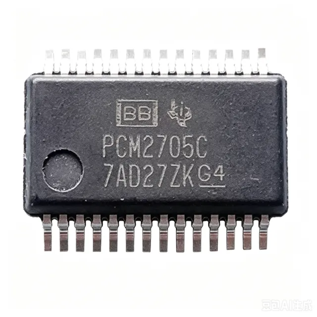
PCM2705C - 98dB SNR Stereo USB DAC with S/PDIF | Texas Instruments
The Texas Instruments PCM2705C is a single-chip stereo audio digital-to-analog converter (DAC) with an integrated USB 2.0 full-speed protocol controller and S/PDIF output. It delivers 98dB SNR and supports both bus-powered and self-powered operation with software control. The device is fully compliant with USB 2.0 specifications and USB Audio Class, requiring no dedicated device driver. It comes in a 28-pin SSOP package, making it ideal for compact audio applications. A USB audio DAC is a digital-to-analog converter that receives digital audio data from a USB host and converts it to analog audio signals. It integrates the USB interface, protocol controller, and DAC core into a single chip, simplifying system design. The PCM2705C sits in the hierarchy of audio converters, specifically as a USB audio interface IC, which is a subset of audio data converters within the broader category of mixed-signal ICs. Key features include a 98dB SNR stereo DAC, S/PDIF output, and support for both bus-powered and self-powered modes. The device also features partially programmable USB descriptors, allowing customization of vendor ID and product ID via an external SPI host. The integrated USB transceiver eliminates the need for external PHY, reducing BOM cost and board space. Technically, the PCM2705C uses adaptive isochronous transfer for audio data, ensuring synchronized playback. The S/PDIF output supports digital audio transmission to external decoders or amplifiers. The device operates from a 3.3V supply and includes an internal PLL for clock generation, minimizing external components. The SSOP-28 package provides a compact footprint suitable for portable and space-constrained designs. Typical applications include USB sound cards, docking stations, gaming headsets, and portable audio interfaces. The device's plug-and-play capability makes it ideal for consumer audio products where driver installation is undesirable. Its low power consumption and small size also suit battery-powered devices. When designing with the PCM2705C, ensure proper decoupling of the 3.3V supply and careful layout of the USB differential pair to maintain signal integrity. The SPI interface for descriptor programming should be configured during initial setup, and the PSEL and HOST pins must be set correctly for the desired operating mode.

PCM3000E - 18-Bit Stereo Audio Codec | Texas Instruments
The Texas Instruments PCM3000E is an 18-bit stereo audio codec with integrated analog-to-digital and digital-to-analog converters, 64-times oversampling, and a 28-pin SSOP package. It accepts single-ended analog voltage inputs and produces single-ended analog voltage outputs, combining stereo recording and playback functions in one low-cost CMOS device. An audio codec is a mixed-signal interface IC that converts between digital audio data and analog voltage signals. In the signal-chain hierarchy, the PCM3000E sits between an audio signal source or microphone front end and a digital audio processor, microphone preamplifier, and analog output amplifier. Its ADC path digitizes stereo analog inputs, while its DAC path reconstructs stereo audio from serial digital data. The integrated converters make it useful in cost-sensitive consumer equipment requiring more functionality than a basic interface controller. Key features include 18-bit ADC and DAC resolution, stereo operation, single-ended analog inputs and outputs, and 64-times ADC oversampling. The DAC section uses an 8-times oversampling digital interpolation filter. A serial interface provides a straightforward connection to digital audio processors, while the integrated codec architecture reduces the number of separate converters required in a stereo audio subsystem. The PCM3000E uses delta-sigma modulation for both conversion paths. Delta-sigma ADCs oversample the analog input and use digital decimation filtering, while the DAC path combines digital interpolation filtering with a single-bit delta-sigma conversion stage. This architecture supports compact, cost-sensitive stereo audio designs and is suited to consumer applications where good performance is required without the complexity of a high-resolution multibit converter. Typical uses include consumer digital audio equipment, portable audio products, stereo cassette and CD-style playback systems, and other sound-processing products. It can also support multichannel designs when multiple codec channels are combined. For digital signal processing, the codec can work with serial audio processors, microcontrollers, or DSPs capable of handling the required master clock, serial data, and control signals. Designers should follow the pin-description table in the manufacturer datasheet when assigning signal paths and decoupling. The analog supply, digital supply, clock, serial interface, and analog-output circuitry require careful partitioning to prevent switching activity and digital coupling from degrading audio performance. The 28-pin SSOP package is compact but has a relatively narrow lead pitch, so PCB assembly and inspection require suitable fine-pitch capability. This page organizes the PCM3000E specifications, pin and package information, product comparisons, engineering guidance, and available drop-in alternatives for faster design review. It also identifies lifecycle and sourcing considerations that should be checked before committing to a new production design.
PCM3000E/2K - 18-Bit Stereo Audio Codec | Texas Instruments
The Texas Instruments PCM3000E/2K is an 18-bit stereo audio codec with two analog-to-digital converters, two digital-to-analog converters, a serial audio interface, and single-ended analog input and output in a 28-pin SSOP package. The codec is intended for cost-sensitive consumer audio equipment requiring one-chip stereo capture and playback. An audio codec is an interface IC that converts analog audio signals into digital data and reconstructs digital audio streams into analog output. In the broader semiconductor hierarchy, PCM3000E/2K belongs to the audio codec family within interface integrated circuits. Combining both conversion directions in one package reduces component count, simplifies board routing, and supports compact consumer audio products such as sound cards, home-audio accessories, and USB audio equipment. The device provides 18-bit stereo conversion, two ADC channels, two DAC channels, and a serial interface. These features make PCM3000E/2K appropriate for designs that need a straightforward stereo signal path rather than a high-channel-count professional codec. Its single-ended analog architecture also simplifies board design by avoiding the balanced input and output networks commonly required by professional audio interfaces. Texas Instruments describes PCM3000 and PCM3001 as low-cost, single-chip stereo codecs fabricated using an advanced CMOS process. Both devices are offered in a compact 28-pin SSOP package. The PCM3001 variant can be pin-programmed for different data formats, whereas the PCM3000 family is primarily intended for applications using its supported serial format. The PCM3000E/2K ordering code identifies the tape-and-reel configuration. Typical uses include USB sound-card signal conditioning, multimedia speaker and headphone interfaces, portable audio accessories, digital recording equipment, and cost-sensitive stereo playback systems. In each case, the device can serve as the central conversion stage between analog transducers and a digital audio controller. Digital audio quality still depends on correct clocking, analog layout, grounding, decoupler placement, and suitable output and input filtering. PCB design should keep analog input and output traces away from digital clock and serial-data paths, while providing a low-impedance ground plane beneath the codec. Follow the manufacturer datasheet for the recommended power, clock, and signal connections. The most important replacement check is not merely the 28-pin SSOP outline but also the exact signal interface, clocking requirements, analog pin functions, and supported data format. This page organizes the PCM3000E/2K specifications, lifecycle information, sourcing path, compatible alternatives, comparison points, and practical integration guidance into one engineering-focused reference. It also distinguishes genuine package-and-interface drop-in options from functionally similar codecs that require different pin assignments or redesigned analog and digital circuitry.
PCM3001E/2K - 18-Bit Stereo Audio Codec | Texas Instruments
The Texas Instruments PCM3001E/2K is an 18-bit stereo audio codec with two analog-to-digital converters, two digital-to-analog converters, and a serial digital audio interface in a 28-pin SSOP package. It combines single-ended analog input and output stages in one device, making it suitable for compact stereo audio systems that require bidirectional analog-to-digital and digital-to-analog conversion. An audio codec is an interface IC that converts analog audio signals into digital data and digital audio data back into analog signals. Within the broader semiconductor hierarchy, the PCM3001E/2K belongs to the audio codec family, which sits under audio interface ICs and interface semiconductors. Its integrated ADC and DAC functions reduce the number of separate converters required in a stereo signal chain while preserving a shared digital audio architecture. The device provides 18-bit stereo conversion, two ADC channels, two DAC channels, and single-ended analog inputs and outputs. Its digital interface is serial, allowing audio data to be transferred between the codec and a digital signal processor, microcontroller, or other audio host. The manufacturer identifies the part as a stereo codec with hardware line-output control, which supports systems requiring analog-output muting or output-path management through hardware control. The PCM3001E/2K is intended for cost-conscious stereo audio equipment where one IC must perform both conversion directions. Its 28-pin SSOP package provides a compact surface-mount footprint while exposing separate analog, digital, power, and control functions. Designers should allocate the board area and decoupling strategy required by the manufacturer application information, especially around analog supply and ground pins. Typical uses include consumer audio equipment, compact stereo playback systems, sound-card analog front ends, multimedia peripherals, and embedded audio products requiring single-ended analog connections. The integrated two-channel ADC and two-channel DAC arrangement allows a system to process captured audio digitally and return processed or stored audio through a line-level output stage. A critical design consideration is maintaining clean, low-impedance analog and digital returns. Follow the pin-description table in the Texas Instruments PCM3001 datasheet when assigning tracks, and place the required bypass capacitors close to their associated supply pins. Keep digital clock and data routes away from the analog input and output paths to reduce crosstalk and conversion error. This page consolidates the device identity, conversion architecture, package details, practical design guidance, and pin-compatible family options for engineers evaluating the PCM3001E/2K. It is intended to support design review, footprint planning, and replacement assessment before the complete Texas Instruments datasheet is consulted for circuit implementation.
PCM3001EG4 - 18-Bit Stereo Audio Codec | Texas Instruments
Texas Instruments PCM3001EG4 is an 18-bit stereo audio codec with two ADCs, two DACs, two input channels, two output channels, and a single-ended analog input/output architecture. The device is packaged in a 28-pin SSOP and uses an 18-bit serial interface to transfer audio data between an analog audio system and a digital processor. Its integrated ADC and DAC channels make it a consolidated interface between analog microphones, line-level sources, audio amplifiers, and digital audio logic. An audio codec is an integrated circuit that converts digital audio data into an analog output and analog audio signals into digital data. In the broader electronics hierarchy, PCM3001EG4 belongs to the audio codec class, then to interface ICs and signal-conversion semiconductors. The PCM3001EG4 combines a stereo ADC path and stereo DAC path in one package, reducing the number of separate converters required in a compact audio design. The principal documented features are 18-bit resolution, stereo operation, two ADC channels, two DAC channels, a serial interface, single-ended analog input/output circuitry, and a 28-pin SSOP package. These features suit compact stereo audio products where both playback and recording paths are needed. The matching ADC and DAC channel count allows a system to use one codec for a two-channel input source and a two-channel output destination, subject to the signal-chain requirements defined by the manufacturer. Technically, the codec separates analog audio conversion from digital transport. Its ADCs sample the incoming analog channels and produce digital data for the host processor, while its DACs receive digital audio and generate analog outputs. The 18-bit serial interface provides the digital link between those converters and the system controller. Designers should treat clocking, data format, analog signal levels, filtering, and power sequencing as the critical implementation considerations rather than treating the codec as a simple standalone audio block. Typical uses include compact stereo recording systems, multimedia audio subsystems, USB or flash-based player accessories, digital mixing equipment, and embedded audio products. For portable or low-voltage systems, power consumption and analog headroom are important; for active studio equipment, channel-to-channel behavior and external analog circuitry require close attention. A microphone preamplifier may be needed when the source level is too low for direct codec input. PCB design should keep analog input and output traces away from high-speed digital clock lines, provide the bypass and filtering components shown in the typical application circuit, and terminate unused analog inputs as directed by the manufacturer. Decoupling should be placed close to the supply pins, while the analog and digital ground strategy must follow the datasheet layout guidance. Proper grounding reduces the chance that codec switching activity couples into the reconstructed audio output. This product page combines the published PCM3001EG4 device identity, channel architecture, resolution, package information, source links, cross-reference findings, and practical design guidance. It also distinguishes documented drop-in relationships from unsupported cross-package options so engineers can make package-aware replacement decisions without assuming that a similar audio codec is electrically interchangeable.
PCM3002E - Low-Power Stereo Audio Codec | Texas Instruments
The Texas Instruments PCM3002E is a low-power stereo audio codec with 16/20-bit resolution, two analog inputs, two analog outputs, and a 24-pin SSOP package. It combines delta-sigma ADCs and DACs with a 20-bit serial audio interface and software-controlled line output, making it suitable for cost-sensitive consumer audio equipment. A stereo audio codec is a mixed-signal semiconductor that converts two analog audio channels into digital data and converts digital audio data back into two analog output channels. In the signal-chain hierarchy, PCM3002E belongs to the audio codec category, combines analog-to-digital converters and digital-to-analog converters, and ultimately supports digital signal processing and audio playback systems. The converter architecture uses delta-sigma modulation with 64-times oversampling. According to the Texas Instruments product information, the ADCs include a digital decimation filter, while the DACs use an 8-times oversampling digital interpolation filter. The 16/20-bit interface supports digital audio formats identified in the family documentation as I2S, L, right-justified I2S, and L/R formats, allowing the device to interface with common audio processors and digital audio buses. The PCM3002 and PCM3003 family is manufactured using an advanced CMOS process and is positioned for cost-sensitive consumer applications where audio performance and low power consumption are important. The 24-pin SSOP package provides a compact surface-mount implementation for consumer audio boards, and the software-controlled line output provides an additional output-control option for system integration. Typical applications include consumer stereo audio systems, portable media equipment, compact digital amplifiers, USB or portable audio accessories, television audio subsystems, and embedded audio interfaces. In each case, the device consolidates two ADCs, two DACs, filtering, and the digital serial interface into one package, reducing the number of separate converter components required on the printed circuit board. When designing a PCB around the PCM3002E, use the manufacturer pin-description table and layout guidance to assign every signal, supply, ground, and reference connection. Decoupling should follow the datasheet recommendations, analog and digital return paths should be routed carefully, and unused inputs should be configured according to the application circuit rather than left electrically unterminated by assumption. This product page combines the device architecture, package information, practical application guidance, sourcing options, and verified equivalent references to support faster component selection and board-level design. It also highlights where an exact replacement is available and when a proposed substitute requires additional engineering verification.
PCM3002E/2K - 20-Bit Stereo Audio Codec | Texas Instruments
The Texas Instruments PCM3002E/2K is a low-power stereo audio codec combining a 20-bit ADC, a 20-bit DAC, and a serial digital audio interface in a 24-pin SSOP package. It supports two single-ended analog inputs, two single-ended analog outputs, 16-bit or 20-bit input and output data, and a maximum sampling rate of 48 kS/s. The codec operates from a 2.7 V to 3.6 V supply and is controlled in software through its serial interface. A stereo audio codec is an interface IC that converts analog audio signals into digital PCM data and converts digital PCM data back into analog audio. It sits between an audio source, such as a microphone or line-level input, and a digital signal processor, microcontroller, or digital audio transmitter. The PCM3002 belongs to the broader codec hierarchy, which includes audio codecs, audio interface ICs, data converters, and interface semiconductors. Key features include 64-times oversampling, a typical signal-to-noise ratio of 90 dB, and 16-bit or 20-bit serial data operation. The two ADC channels use single-ended voltage inputs, while the two DAC channels provide single-ended analog outputs. These characteristics make the device suitable for compact stereo audio paths where a separate ADC, DAC, and interface circuit would otherwise be required. Internally, the codec integrates antialiasing filtering with its oversampling conversion architecture. The serial interface supports I2S, L-format, and right-justified data formats according to the cross-reference information for the PCM3002 family. Its 3.6 V maximum supply operation supports low-voltage digital audio systems, while the integrated converters reduce component count and simplify synchronization between the analog and digital sections. Typical applications include digital recording equipment, powered speakers, compact consumer audio products, sound-card inputs, industrial audio terminals, and embedded audio systems that require stereo conversion at 48 kS/s. The software-control architecture is particularly useful when a host processor must select operating modes, adjust gain, or manage system functions through the serial control interface. PCB design should treat the analog input and output paths as sensitive signal routes. Keep analog and digital ground handling consistent with the manufacturer's recommended layout, place bypass and interface components close to their associated pins, and route high-speed serial clock and data lines away from the analog inputs. Adequate filtering and stable 3.6 V power are essential for repeatable low-noise operation. This page combines the manufacturer specifications with practical interface guidance, application-oriented design notes, and a focused comparison of pin-compatible family options. It is intended to help engineers select the correct codec variant, plan its analog and digital implementation, and evaluate replacement choices without overlooking control-mode or data-format differences.
PCM3002EG - 20-Bit Low-Power Stereo Codec | TI
The Texas Instruments PCM3002EG is a low-power 20-bit stereo audio codec with two analog-to-digital converters, two digital-to-analog converters, single-ended analog inputs and outputs, and software-controlled line output. The device is packaged in a 24-pin SSOP for conventional surface-mount audio processing designs. An audio codec is an integrated circuit that converts analog audio signals into digital data and converts digital audio data back into analog signals. Its role within an audio signal chain is wider than that of a standalone ADC or DAC: the codec integrates conversion circuitry, a digital audio interface, analog input and output channels, and the control functions needed to manage a compact stereo audio path. PCM3002EG belongs to the broader hierarchy of audio codec, interface IC, data converter, and power-management-assisted signal-chain IC. The PCM3002EG combines 2 ADC channels and 2 DAC channels with 20-bit resolution. Its single-ended analog input architecture supports two stereo input channels, while its two DAC outputs support stereo playback. The line-output stage includes software control, allowing an audio system to manage output behavior through the digital control interface. The low-power designation makes the codec relevant to compact audio equipment where energy efficiency and integration are important. The PCM3002EG uses a 20-bit serial audio interface, according to the product listing for this exact ordering code. This interface connects the codec to a digital signal processor, microcontroller, application processor, or other audio controller. The 24-pin SSOP package provides a defined PCB footprint while keeping the analog and digital functions in one component. Designers should follow the manufacturer datasheet for the exact clock, format, control, voltage, and de-identification details when laying out the circuit. Typical applications include digital audio recording, compact stereo playback equipment, audio capture modules, multimedia appliances, and embedded systems that need both microphone or line-level input and line-level output. In a recording path, the two ADC channels digitize left and right analog sources. In a playback path, the two DAC channels reconstruct stereo audio. Software-controlled line output is useful when the system needs configurable output behavior under processor control. For a new design, verify the codec's supported sample rate, operating voltage, master-clock requirements, analog input range, digital interface format, and pin-level bypass recommendations against the current manufacturer datasheet. These details determine whether the PCM3002EG can be connected directly to the chosen host processor or whether level-shifting, filtering, or additional clock circuitry is required. This page consolidates the exact PCM3002EG ordering information, manufacturer product resources, technical attributes, verified drop-in comparison requirements, and practical integration guidance. It is designed to help engineers evaluate the 20-bit stereo codec, inspect its SSOP footprint, confirm interface requirements, and plan sourcing through a structured request-for-quote workflow.
PCM3003E - Low-Power Stereo Audio Codec | Texas Instruments
Texas Instruments PCM3003E is a low-power stereo audio codec with 16-bit or 20-bit resolution, single-ended analog inputs and outputs, and a 24-pin SSOP package. The device operates from a 2.7 V to 3.6 V analog supply and supports an industrial temperature range of -25 °C to +85 °C. An audio codec is an integrated interface that converts between analog audio signals and digital PCM data. The PCM3003E combines stereo analog-to-digital and digital-to-analog conversion functions in one IC, making it suitable for compact consumer audio equipment where component count, power consumption, and board area are important. Its digital audio interface and analog signal path support equipment such as consumer audio systems, portable products, and compact multimedia devices. The PCM3003E offers selectable 16-bit or 20-bit operation, providing flexibility for designs that balance conversion resolution against system data rate and storage requirements. Its line output includes hardware control, allowing the output stage to be managed according to the product architecture. A single-ended analog interface can simplify PCB routing, although grounding and signal-return design remain important for low-noise performance. The codec is manufactured using an advanced CMOS process and is intended for cost-sensitive consumer applications that require good audio performance without a high-complexity audio interface. The 24-pin SSOP package supports conventional surface-mount assembly and is compatible with automated production processes. System designers should follow the manufacturer pin-description table and recommended application circuit when assigning PCB tracks. Typical PCM3003E applications include stereo audio playback and capture, consumer media equipment, compact sound systems, and embedded audio products. The 2.7 V to 3.6 V operating range supports low-voltage digital platforms, while the -25 °C to +85 °C temperature range covers industrial environments. External decoupling, controlled analog grounding, and careful clock routing should be treated as core parts of the analog design. This product page combines manufacturer specifications, packaging information, application guidance, and engineering comparisons. It also distinguishes the PCM3003E from identified family variants and highlights the design checks that matter when integrating a low-power stereo codec into a mixed-signal PCB.
PCM3003E/2K - 20-Bit Stereo Audio Codec | Texas Instruments
The Texas Instruments PCM3003E/2K is a low-power, single-chip stereo audio codec with a 20-bit ADC, 20-bit DAC, single-ended analog inputs and outputs, and hardware control in a 24-pin SSOP package. The device operates from 2.7 V to 3.6 V and supports 16-bit or 20-bit input and output data through its serial interface. An audio codec is an interface IC that combines analog-to-digital and digital-to-analog conversion with the digital audio interface required to exchange samples with a host processor. The PCM3003 belongs to the broader codec hierarchy of audio interface ICs and power-management-dependent mixed-signal devices, bridging microphone-level or line-level analog signals and a digital audio bus. The PCM3003E/2K provides a monolithic stereo ADC and DAC, 64-times oversampling, single-ended voltage inputs, and integrated antialiasing filtering. Its specified THD+N reaches -86 dB, making it suitable for consumer audio equipment where signal-chain fidelity must coexist with a compact, low-power implementation. The hardware-control interface simplifies control of operating functions without relying entirely on software commands. The 20-bit internal converters support 16-bit or 20-bit input and output data, allowing the digital interface to match different source and destination formats. The codec is designed around a 2.7 V to 3.6 V supply range, so system-level audio rails must remain within these limits. Its SSOP-24 package supports conventional surface-mount assembly while preserving compatibility with compact audio boards. Typical applications include stereo line-input and line-output processing, digital audio recording interfaces, multimedia equipment, and compact consumer audio products. In these systems, the ADC can capture single-ended analog input channels, while the DAC and line-output circuitry can provide analog playback from digital audio data. The integrated filtering and oversampling reduce the amount of external analog filtering required around the converters. The main design consideration is to treat analog, digital, and ground connections as separate signal paths. Keep serial-clock and data traces away from the analog inputs, provide local bypass capacitance at the supply pins, and use a quiet ground reference for the analog return path. Component values and supported clock configurations should be selected directly from the manufacturer datasheet and its recommended application circuit. This page consolidates the exact PCM3003E/2K ordering information, electrical specifications, package details, practical applications, and verified drop-in alternatives. It also provides procurement guidance and design notes intended to support faster engineering evaluation while preserving the distinction between documented device ratings and application-specific requirements.