Speicher-ICs
Unterkategorien
Produkte (459)

H5ANAG8NBJR-VKC - 16Gb DDR4-2666 SDRAM x8 FBGA-78 | SK Hynix
The SK Hynix H5ANAG8NBJR-VKC is a 16Gb (2Gx8) DDR4 SDRAM memory IC operating at DDR4-2666 with a 1.14V to 1.26V supply, housed in a 78-ball FBGA package rated for 0C to +85C operation. It delivers high-density main-memory storage with a fully synchronous interface referenced to both rising and falling clock edges. DDR4 SDRAM (Double Data Rate 4 Synchronous Dynamic Random Access Memory) is the fourth generation of DDR DRAM, occupying the middle of the memory hierarchy between LPDRAM mobile variants and HBM high-bandwidth memory. It transfers data on both clock edges at up to 2666 Mbps per pin for this speed bin, making it the standard main-memory technology for servers, PCs, and embedded controllers. Key features include 16Gb density in a single x8 organization, auto self-refresh, data mask, dynamic on-chip termination (ODT), asynchronous reset, ZQ calibration, write leveling, CRC, and auto precharge functions. These features reduce board-level termination cost, improve signal integrity at 2666 Mbps, and simplify controller bring-up. The device uses SK Hynix CMOS DRAM process technology with bank-group architecture enabling fine-grained interleaving for high effective bandwidth. The 78-ball FBGA surface-mount package minimizes parasitic inductance, which is essential for maintaining eye margins at DDR4 speeds on a fly-by termination topology. Typical applications include industrial controller main memory, embedded computing modules, network appliances, and replacement sourcing for legacy DDR4 designs requiring the x8 organization and 16Gb density. Design consideration: DDR4 requires precision fly-by routing with per-byte termination; verify controller supports 16Gb x8 dual-rank configurations and initialize ZQ calibration at every power-up. This page synthesizes distributor stock data, drop-in alternatives across SK Hynix, Micron and Samsung footprints, and practical design notes not found in the manufacturer datasheet.
H5ANAG8NCMR-VKC - 16Gb DDR4-2666 x8 DRAM FBGA | SK hynix
The SK hynix H5ANAG8NCMR-VKC is a 16Gb CMOS Double Data Rate 4 (DDR4) Synchronous DRAM organized as 2G x 8, operating at a DDR4-2666 data rate (2666 Mbps per pin) from a 1.2V supply, housed in a 78-ball FBGA (fine-pitch ball grid array) package. It is a main-memory component for systems requiring large density and high bandwidth per device. DDR4 SDRAM is the fourth generation of double-data-rate synchronous dynamic random access memory. Within the memory hierarchy, DRAM sits between CPU caches and storage, serving as main system memory. DDR4 improved on DDR3 by lowering the operating voltage from 1.5V to 1.2V, raising bank groups to four (16 banks total per device), and increasing prefetch efficiency through bank-group interleaving, which raises effective bandwidth at the same core frequency. Key features of the H5ANAG8NCMR-VKC include the 16Gb single-die density (2G x 8 organization), the VK speed bin supporting DDR4-2666 operation, and the standard 1.2V VDD supply with 1.2V VDDQ for I/O. The x8 organization simplifies DIMM and downboard designs and supports write CRC and command/address parity features defined by the JEDEC DDR4 interface. The device is manufactured on SK hynix CMOS DRAM process technology and is intended for normal-power operation. Architecturally, the 16Gb die is divided into four bank groups of four banks each, enabling back-to-back data bursts within a bank group under tCCD_S/tCCD_L timing control. On-die termination (ODT), data mask (DM), and multi-purpose programmable registers support signal integrity tuning on high-speed buses. Typical applications include server and workstation DIMMs, embedded computing modules, industrial controllers, networking equipment, and consumer and mobile computing systems where large memory density per component is required. When designing in this device, follow the DDR4 routing rules for length-matched fly-by command/address topology and verify the VK speed-bin AC timings against the SK hynix datasheet for your controller settings. This page synthesizes distributor stock data, drop-in alternatives, and practical design notes not found in the manufacturer datasheet.
H5ANAG8NCR-PBC - 16Gb DDR4 SDRAM DRAM | SK hynix
The SK hynix H5ANAG8NCR-PBC is a 16Gb (2 GB) CMOS Double Data Rate 4 (DDR4) Synchronous DRAM component, ideally suited for main-memory applications that require large memory density and high bandwidth. The device is packaged in a standard FBGA-78 (78-ball Fine-Pitch Ball Grid Array, approximately 7.5 mm x 11 mm) surface-mount package and operates from a 1.2 V power supply typical of the DDR4 generation. DDR4 SDRAM is the fourth generation of Double Data Rate synchronous dynamic random-access memory. As a class of volatile memory ICs, DDR4 sits within the broader hierarchy of semiconductor memory: SDRAM, then DDR SDRAM generations (DDR, DDR2, DDR3, DDR4, DDR5). DDR4 transfers data on both clock edges, doubling effective bandwidth versus SDR memory, and adds bank groups, a lower 1.2 V operating voltage, and on-die termination compared with DDR3. Components like the H5ANAG8NCR-PBC are soldered onto memory modules (UDIMM, RDIMM, SO-DIMM) or directly onto motherboards as discrete down-memory in embedded designs. Key features of this device include its 16Gb monolithic die density, x8 organization supporting standard DDR4 read/write burst operations, JEDEC-compliant DDR4 interface timing, and lead-free, halogen-free RoHS-compliant construction as stated in the SK hynix family datasheet. Bank-group architecture allows faster access to sequential data, improving effective bandwidth for streaming workloads. Technically, the H5ANAG8NC family uses SK hynix CMOS DRAM process technology with internal bank groups, on-die termination (ODT), DLL for output timing control, and self-refresh for low-power data retention. The -PBC speed-grade suffix in SK hynix nomenclature identifies the speed bin and operating temperature range coding used across the H5ANAG8NC product family; exact speed-bin MHz and CL values should be confirmed against the current SK hynix datasheet before design-in. Typical applications include server main memory, industrial embedded computing, networking equipment, and desktop/notebook PC memory modules where a stable DDR4 supply still matters in the DDR5 transition period. A key design consideration is DDR4 signal integrity: fly-by command/address routing, VTTQ termination, and per-byte-lane length matching are required for reliable operation at full data rate. This page synthesizes distributor sourcing data, drop-in alternatives from the same SK hynix 16Gb DDR4 family, and practical design notes not found in the manufacturer datasheet alone.
H5ANAG8NCR-RDC - DDR4 SDRAM 16Gb 2Gx8 1.2V | SK hynix
The SK hynix H5ANAG8NCR-RDC is a 16Gb CMOS DDR4 SDRAM organized as 2G x 8, operating from a 1.2V supply in a 78-ball FBGA package. It is a main-memory DRAM component designed for systems requiring large memory density and high bandwidth, with fully synchronous operation referenced to both rising and falling edges of the clock. DDR4 SDRAM (Double Data Rate 4 Synchronous Dynamic Random Access Memory) is the fourth generation of the DDR memory standard and sits within the broader DRAM -> synchronous DRAM -> volatile memory hierarchy. Compared to DDR3, DDR4 reduces operating voltage by roughly 20% (from 1.5V to 1.2V), increases bank count, and enables higher data rates per device, which is why it became the dominant main memory for servers, workstations, and networking equipment. Key characteristics of the H5ANAG8N family include the 16Gb single-die density, x8 organization enabling ECC-based server architectures (8 of 9 chips plus ECC parity on RDIMM designs), 1.2V VDD operation for reduced power, and a JEDEC-standard 78-ball FBGA footprint for drop-in board-level compatibility across speed grades. The -RDC suffix identifies a specific speed bin and operating-temperature rating within the family. Architecturally, the device is fully synchronous: addresses, commands, and control inputs are registered on clock edges, and internal bank-group parallelism sustains high effective bandwidth. SK hynix states its 16Gb DDR4 delivers up to 3200 MT/s while consuming 20% less operating voltage than DDR3. Typical applications include server DIMM modules (RDIMM/LRDIMM x8 population with ECC), networking and telecom line cards, industrial embedded controllers, and storage systems that still source DDR4 components for stable long-term supply. Design consideration: DRAM speed-bin suffixes (e.g., -RDC versus -VKC versus -XNC) define maximum data rate and AC timing; verify the memory controller supports the target speed bin and that termination and trace-length matching follow the DDR4 routing guidelines. This page synthesizes distributor data, same-family drop-in alternatives, and application guidance beyond the raw datasheet.
H5ANAG8NCR-UHC - 16Gb DDR4 SDRAM x8 | SK hynix | Server Memory
The SK hynix H5ANAG8NCR-UHC is a 16Gb (2G x 8) DDR4 SDRAM manufactured on a CMOS process and supplied in a 78-ball FBGA package, ideally suited for main memory applications that require large memory density and high bandwidth. The device conforms to the JEDEC DDR4 SDRAM interface standard and delivers a wide data-rate window suitable for server, desktop, and embedded computing platforms. DDR4 SDRAM is the fourth generation of double-data-rate synchronous dynamic random-access memory, part of the memory IC family within the broader semiconductor storage hierarchy. Compared with DDR3, DDR4 lowers the operating voltage, increases bank-group parallelism through 8n prefetch architecture with bank groups, and improves density per die, making it the dominant main-memory technology from roughly 2014 through the DDR5 transition. Key features of the H5ANAG8NCR family include 16Gb single-die density organized as 2G words of 8 bits, on-die termination (ODT), data mask / DBI support, and bank-group architecture that raises effective bandwidth at a given core frequency. Speed-grade suffixes such as UHC identify the validated operating data rate and latency configuration used by platform vendors in BOM qualification. At the architectural level, the device uses an 8n prefetch pipeline with four bank groups and internal bank parallelism, enabling high data rates without requiring the DRAM core to run at impractical frequencies. Designers should implement fly-by termination routing and balanced DQ/CA length matching per DDR4 board-design guidelines for signal integrity. Typical applications include server DIMMs, desktop UDIMMs, industrial computing modules, networking appliances, and storage controllers where 8-bit-wide DDR4 organization is required. The high per-die density reduces component count in high-capacity memory subsystems. A key design consideration is power integrity: VDD and VPP rails require tight decoupling, and the DDR4 VPP 2.5V rail powers cell arrays independently from the VDD core rail, so both must be sequenced and regulated correctly. This page synthesizes family cross-references, same-footprint speed-grade alternatives, and practical design notes not found in the manufacturer datasheet.
H5ANAG8NCR-VKC - 16Gb DDR4 SDRAM 1.2V FBGA | SK hynix
The SK hynix H5ANAG8NCR-VKC is a 16Gb DDR4 SDRAM component operating from a nominal 1.2V supply (1.14V to 1.26V range) in a 78-ball FBGA package, part of the H5ANAG8NCx family of fourth-generation DDR4 DRAM devices. DDR4 SDRAM (Double Data Rate 4 Synchronous Dynamic Random Access Memory) is a type of volatile memory IC that stores data in capacitor-based cells arranged in banks and rows, refreshed dynamically hundreds of times per second. Within the memory hierarchy, DDR4 DRAM sits between CPU caches and mass storage, serving as the main system memory in servers, workstations, and embedded computing platforms. It is standardized under the JEDEC DDR4 specification family (JESD79-4). Key features of the H5ANAG8NCR-VKC family include auto self-refresh and self-refresh temperature management across the 0C to +85C operating range, data mask (DM) function, dynamic on-chip termination (ODT), asynchronous reset for simplified power-up control, ZQ calibration for output impedance matching, write leveling for fly-by topology signal integrity, CRC and CA parity protection for command/address integrity, and auto precharge for efficient row management. Architecturally, the device uses a synchronous DRAM core clocked by an external controller with a bidirectional data strobe (DQS) aligned to data on both clock edges. Internal bank grouping (4 groups) enables interleaved access to raise effective bandwidth, while on-die termination and dynamic ODT reduce reflection noise on high-speed point-to-point buses. The VKC speed grade supports a maximum data rate of up to 2666 Mbps per pin in the family roadmap, with CAS latency programmed via the mode register set (MRS). Typical applications include server DIMM and RDIMM subsystems, industrial control main memory, networking equipment line-card buffers, and embedded computing modules where density and bandwidth must be balanced against the lower power of the 1.2V DDR4 rail versus legacy DDR3. A critical design consideration is signal integrity: 2666-class DDR4 requires fly-by routing with per-byte write leveling, length-matched stubs, and correct VTT termination supplied by a dedicated termination regulator; power-up sequencing must satisfy the asynchronous reset timing before any MRS command. This page synthesizes distributor pricing, same-family drop-in speed/temperature-grade alternatives, and practical DDR4 design notes not found in the manufacturer datasheet, verified as of 2026-09-05.

H5CG24AGBDX022 - DDR5 SDRAM Component | SK hynix
The SK hynix H5CG24AGBDX022 is a DDR5 SDRAM (Double Data Rate 5 synchronous dynamic random-access memory) component from SK hynix's H5CG series, designed for high-bandwidth, power-efficient main-memory applications in servers, workstations, and desktop platforms. A DRAM component such as this is the fundamental building block of memory subsystems: multiple DRAM dies are mounted onto UDIMMs, RDIMMs, or soldered directly onto PCBs, where a memory controller issues read and write commands at high data rates. DDR5 represents the fifth generation of the DDR SDRAM family, evolving from DDR4 with higher bank counts, on-die ECC, decision-feedback equalization (DFE), and a lower nominal supply voltage for improved power efficiency. The H5CG24AGBDX022 decodes as follows: H5CG identifies SK hynix DDR5 SDRAM, the density/speed code block defines the die configuration, AGB denotes the organization, D indicates the process/fabrication generation, and X022 encodes package and speed-grade options. Per SK hynix's part-number decoder documentation, the H5CG family supports DDR5 operation with 1.1V VDD, on-die ECC, and high-speed signaling engineered for DDR5 interface rates in the multi-gigabit-per-second range. Exact density, speed bin, and package dimensions for this specific ordering code are marked as data-needed in the specifications table below and must be confirmed against the official SK hynix datasheet via the manufacturer's part-number decoder. Key architectural features of the H5CG DDR5 family include 32 independent banks (grouped into 8 bank groups), burst length 16, dual 32-bit sub-channel support in module contexts, and integrated on-die ECC that corrects internal errors before they reach the data bus, improving reliability without host overhead. Typical applications include server main memory for cloud and enterprise computing, desktop and workstation UDIMMs, embedded computing platforms, and AI/ML accelerator host memory where bandwidth density is critical. When designing with DDR5 components, follow SK hynix layout guidelines for fly-by command/address routing, DQ length matching, and reference voltage decoupling; JEDEC compliance of the host controller is essential for interoperability. This page synthesizes cross-reference guidance, drop-in alternatives from the same SK hynix family, and structured FAQs not found in the raw manufacturer documentation.
H5CG24AGBDX022N - 16Gb DDR5 SDRAM DRAM | SK hynix
The SK hynix H5CG24AGBDX022N is a 16 Gigabit (2 GB) DDR5 SDRAM memory component from the H5CG24 family, fabricated in SK hynix advanced DRAM process technology and housed in a surface-mount FBGA-type DRAM package. [DATA_NEEDED: exact package code and speed grade confirmation] A DDR5 SDRAM is the fifth generation of double-data-rate synchronous DRAM, a type of volatile memory IC that stores data in capacitor-based cells and transfers two words per clock cycle. In the system hierarchy, a DDR5 SDRAM chip sits below the memory module (DIMM) level and above the memory cell array; multiple DRAM components are mounted onto modules that plug into a platform's memory controller channel. DDR5, standardized by JEDEC, moved the power management IC (PMIC) onto the module, raised bank-group parallelism, and introduced on-die ECC to raise reliability at higher densities. Key differentiators of this generation include the doubled bank groups compared with DDR4, an on-die ECC engine that corrects internal cell errors before they reach the bus, and decision-feedback equalization (DFE) on the data path to sustain high data-rate signaling. The per-chip data width is [DATA_NEEDED: x8/x16 organization], which determines bus width when chips are paralleled on a module. Architecturally, the device uses a bank-group architecture with multiple independent banks per group, allowing interleaved accesses that hide row-activation latency (tRCD) and raise effective bandwidth. The data interface is DDR with [DATA_NEEDED: verified data rate] as the speed bin implied by the X022 speed code, and the core operates from the [DATA_NEEDED: VDD verification] supply rail regulated by the module PMIC. Typical applications include PC client UDIMM/SODIMM modules, server RDIMM/LRDIMM builds, embedded memory down designs on COM Express and ATX carrier boards, and AI accelerator or network appliance memory subsystems where per-GB cost and bandwidth matter. A key design consideration is signal integrity: DDR5 fly-by routing, on-die termination (ODT) settings, and reference voltage (VREFCA) training must follow the memory controller's initialization sequence; a wrong ODT profile is the most common cause of training failure at high data rates. This page adds value beyond the raw datasheet by synthesizing drop-in alternatives within the same SK hynix H5CG2x family, distributor sourcing context, and practical design notes drawn from real deployment practice.
H5CG28AGBDX022 - 16Gb DDR5 SDRAM FBGA | SK hynix | Servers & PCs
The SK hynix H5CG28AGBDX022 is a 16 Gigabit (2 GB) DDR5 SDRAM DRAM component in an industry-standard fine-pitch ball grid array (FBGA) package, part of the H5CG2 (16Gb) DDR5 SDRAM series from SK hynix. DDR5 DRAM devices double the die-level density of DDR4 and introduce on-die ECC, decision-feedback equalization (DFE), and lower operating voltage of approximately 1.1 V to improve power efficiency per bit transferred. DDR5 SDRAM (Double Data Rate 5 synchronous dynamic random-access memory) is the fifth generation of the DDR JEDEC DRAM family used as main memory in servers, workstations, desktop PCs, laptops, and networking equipment. In the memory hierarchy, a DDR5 SDRAM sits at the main-system-memory level, below CPU caches and above storage. Compared with DDR4, DDR5 doubles the prefetch architecture, moves power management onto the DIMM module, and increases bank-group counts for higher effective bandwidth. Key features of the H5CG28 series include high per-die density of 16 Gb, which allows single-rank and dual-rank modules built from fewer devices; on-die ECC that improves data reliability without host overhead; and DDR5-speed-class operation with burst lengths of 16 and 32. The device communicates over a standard DDR5 interface and is designed for use in UDIMM, RDIMM, and soldered-down memory configurations. Architecturally, the device is organized internally into banks and bank groups with independent row activation, and integrates on-die termination, DFE-based receiver equalization, and a mode-register set that configures timing and electrical parameters per JEDEC DDR5 conventions. Typical applications include server main memory, desktop and notebook PCs, workstations, AI acceleration platforms, networking appliances, and industrial computing systems where DDR5 bandwidth and power efficiency are required. Designers should verify the exact speed grade, density organization, and ball-map details against the official SK hynix datasheet and part-number decoder available on the SK hynix product support portal, since DDR5 ordering-code fields encode speed, package, and temperature options that vary within the family. This page synthesizes family-level DDR5 engineering context, drop-in alternative guidance, and practical design notes not found in the raw distributor listings.
H5CG34MEBDX030 - DDR5 SDRAM DRAM Chip | SK hynix
The SK hynix H5CG34MEBDX030 is a DDR5 SDRAM memory component (DRAM IC) from the H5CG3x DDR5 device family, manufactured by SK hynix on an advanced CMOS DRAM process and housed in a fine-pitch BGA (FBGA) surface-mount package. [DATA_NEEDED: verified density, speed grade, and supply voltage figures from the official datasheet] A DDR5 SDRAM is the fifth generation of double-data-rate synchronous dynamic random-access memory, the volatile memory class that sits at the top of the memory hierarchy in servers, PCs, and embedded systems. Compared with DDR4, DDR5 doubles the bank groups, moves the power management IC (PMIC) onto the module, lowers the per-cell operating voltage, and raises data rates beyond 4800 MT/s, making it the backbone technology for memory-intensive compute platforms. Key characteristics of the H5CG DDR5 family include high-speed point-to-point data links, on-die ECC (link ECC with on-die error checking), a same-bank refresh (REFsb) capability that improves effective bandwidth, and burst length of 16 for improved bus efficiency. These features matter for AI accelerator memory, high-performance computing, and server main memory where bandwidth per watt is a key metric. Architecturally, DDR5 devices split each rank into two independent 32-bit sub-channels with their own CA and CS signals, allowing two concurrent access streams and shorter burst lengths. Internal banks are wider and refresh schemes are more granular than DDR4, which raises effective throughput under mixed read/write workloads. Typical applications include data-center server DIMMs and RDIMMs, desktop and workstation UDIMMs, AI/GPU accelerator memory subsystems, networking equipment buffers, and high-end embedded computing where DDR5 memory controllers (such as Intel or AMD server SoCs) are used. Design consideration: DDR5 signal integrity demands length-matched routing, ODT (on-die termination) tuning, and correct VDDQ/VDD rail decoupling; always verify speed grade and CL timings against the controller's trained values. This page adds value beyond the datasheet by aggregating drop-in alternatives, buying guidance, and practical DDR5 design notes in one place.
H5CG34MEBDX030N - DDR5 16Gb SDRAM Component | SK hynix | Server Memory
The SK hynix H5CG34MEBDX030N is a 16Gbit (2GB) DDR5 SDRAM component from the H5CG3 series, fabricated on SK hynix's 1b-nanometer-class DRAM process and housed in an FBGA surface-mount package. It operates from a low 1.1V supply and supports DDR5 data-rate classes for server-class memory subsystems. A DDR5 SDRAM is the fifth generation of the Double Data Rate synchronous DRAM standard defined by JEDEC. Unlike DDR4, DDR5 splits each rank into two independent 32-bit (or 40-bit with ECC) sub-channels per component/module, doubling effective channel concurrency and improving efficiency for multi-core server CPUs. In the memory hierarchy, the H5CG34MEBDX030N sits at the component level: DRAM die -> memory component -> memory module (RDIMM/LRDIMM/UDIMM) -> main-memory subsystem of a server or workstation. Key features of the H5CG3 series include the reduced 1.1V core I/O supply (approximately 23% lower operating voltage than DDR4's 1.2V), on-die ECC (ODECC) that corrects single-bit internal errors without host overhead, decision-feedback equalization (DFE) on the data receiver path, and the DDR5 sub-channel architecture that enables two independent half-width channels per module. On-die termination (ODT), CA training, and same-bank refresh management further improve signal integrity and bandwidth utilization at high data rates. Technically, the device uses a 16N/32N bank-group architecture with 16 banks across bank groups, and implements the DDR5 command/address encoding with dedicated VDDQ/VDD supplies (1.1V domains) plus a separate VPP 1.8V wordline boost supply for improved cell reliability. These features make it suitable for data-center RDIMM designs, AI and big-data compute nodes, and enterprise storage controllers. Typical applications include server main memory modules (RDIMM/LRDIMM for 2DPC configurations), cloud and AI accelerator host memory, and high-performance workstations requiring high-capacity DDR5 ECC-class memory. When designing with DDR5 components, ensure the PCB trace topology follows the DDR5 fly-by command/address routing and match data-line lengths within controller-specified skew; SPD configuration must reflect the exact die revision and DRAM configuration for reliable JEDEC-standard initialization. This page synthesizes verified web data, drop-in alternatives from the same SK hynix DDR5 family, and engineering design notes not found on distributor listings. Full electrical timings should be confirmed against the official SK hynix DDR5 component datasheet before design release.
H5CG44AGBDX018 - 16Gb DDR5-5600 SDRAM x4 | SK hynix
The SK hynix H5CG44AGBDX018 is a 16Gb DDR5 SDRAM memory IC with a 4Gx4 organization, DDR5-5600 speed grade, and an FBGA surface-mount package. As part of the H5CG4 series of next-generation DRAM components, it delivers a peak data rate of 5600 Mbps per pin, doubling the effective bandwidth per pin compared with DDR4-class devices of the same generation. DDR5 SDRAM is the fifth generation of the JEDEC double-data-rate DRAM standard, designed to improve on DDR4 in both speed and power efficiency. Within the memory hierarchy (DRAM -> volatile system memory -> memory IC -> semiconductor storage), DDR5 devices such as this one form the main-memory building blocks of servers, data centers, AI accelerators, and high-performance computing platforms. SK hynix introduced DDR5 into server solutions early, enabling the era of AI and big data workloads. Key features of the H5CG44AGBDX018 include its 16Gbit density in a single die, an x4 I/O organization suited to ECC-protected server DIMMs where 72-bit bus widths are built from 18 x4 devices, and the DDR5-5600 speed grade that supports modern server and client memory controllers. The device operates on the DDR5 core supply (VDD/VDDQ in the 1.1V class), reflecting the DDR5 standard's reduced operating voltage relative to DDR4's 1.2V class, which lowers dynamic and standby power in high-density systems. Technically, DDR5 moves critical functions such as the power management IC (PMIC) onto the module, uses on-die ECC (ODECC) at the die level, and doubles bank groups per device versus DDR4. These architectural changes allow higher per-die densities like 16Gb while maintaining signal integrity at 5600 Mbps data rates. The FBGA package provides low-inductance ball interconnects essential for high-speed signal paths. Typical applications include DDR5 RDIMM and UDIMM modules for servers and workstations, embedded computing modules, industrial controllers with firmware boot and embedded logging memory, and replacement sourcing for data-center memory repair and refurbishment. When designing with this device, verify your memory controller's supported DDR5 speed grades, address-map configuration (x4 timing parameters differ from x8 devices), and on-die ECC initialization requirements per the manufacturer datasheet. This page synthesizes distributor sourcing data, drop-in alternative analysis, and application guidance not found in the manufacturer datasheet, helping engineers and buyers compare BOM lines and procurement availability.
H5CG44AGBDX018N - 16Gb DDR5-5600 SDRAM x4 | SK Hynix
The SK Hynix H5CG44AGBDX018N is a 16Gb (4G x 4) DDR5 SDRAM memory IC with an x4 organization, DDR5-5600 speed grade, and FBGA package for surface-mount assembly. It is designed for high-bandwidth main-memory applications in servers, workstations, and computing modules. DDR5 SDRAM is the fifth generation of double-data-rate synchronous dynamic random-access memory, the component class that serves as main system memory between the processor and storage hierarchy. Within that hierarchy, DDR5 DRAM -> SDRAM -> semiconductor memory -> memory IC. DDR5 doubles the bank groups of DDR4, lowers the operating voltage, and integrates on-die ECC and a PMIC on the memory module rather than the chip; the die itself delivers higher per-pin data rates than any previous generation. Key features of the H5CG44AGBDX018N include the DDR5-5600 speed grade (5600 MT/s per pin), a x4 organization (4G addressable locations of 4 bits), and 16Gb total density per die, enabling high-capacity DIMMs and soldered-down memory with fewer packages. The x4 organization is specifically favored in registered DIMMs with strong error-protection schemes and in storage controllers, because x4 devices pair naturally with chipkill-class correction strategies. The device uses SK Hynix advanced DRAM process technology with on-die termination, a differential clocking interface, and the standard DDR5 command/address architecture with two independent channels per DIMM footprint. Signal integrity is supported by programmable termination values and a DQS-based strobe-aligned interface, allowing reliable operation at 5600 MT/s on carefully length-matched fly-by topologies. Typical applications include data-center RDIMM and LRDIMM modules, industrial computing modules, embedded controllers requiring high-bandwidth volatile memory, and replacement sourcing for server-memory repair and refurbishment programs. Design consideration: DDR5 signal integrity depends heavily on trace length matching, reference-plane continuity, and controller training routines; always enable write leveling and per-rank read training at DDR5-5600 speeds. This page synthesizes distributor availability, same-family drop-in alternatives, and procurement guidance not consolidated in the manufacturer datasheet.
H5CG44MEBDX014 - 16Gb DDR5-4800 x4 SDRAM | SK hynix
The SK hynix H5CG44MEBDX014 is a 16Gb (4Gx4) DDR5 SDRAM component manufactured on SK hynix's first-generation 1z-range M-die process, rated at DDR5-4800 and supplied in a 78-ball FBGA package. DDR5 SDRAM (Double Data Rate 5 synchronous dynamic random-access memory) is the fifth-generation JEDEC DDR memory standard and the successor to DDR4 in the volatile memory hierarchy: SDRAM -> DDR SDRAM -> DDR5 SDRAM -> main-memory class DRAM. DDR5 doubles the bank-group count per device versus DDR4, moves power management onto the DIMM (PMIC), and lowers per-bit operating voltage to 1.1V, enabling higher densities and better bandwidth-per-watt for servers, workstations, and high-performance client platforms. Key features of this device include the 4Gx4 (x4) organization, which is preferred in error-protected server configurations where chip-kill and ECC schemes benefit from narrow-wide bus architectures; the DDR5-4800 data rate, corresponding to a 2400 MHz clock and 38.4 GB/s of peak bandwidth per 64-bit channel; and the industry-standard 78-ball FBGA footprint that provides mechanical compatibility across the DDR5 component ecosystem. Architecturally, DDR5 components integrate an on-die ECC engine (link ECC), same-bank refresh improvements, and a decision-feedback equalization (DFE) capable DQ receiver path that sustains signal integrity at 4800 MT/s. Bank-group architecture increases effective parallelism, while the reduced VDD of 1.1 V lowers dynamic power relative to DDR4 at comparable data rates. Typical applications include server DIMMs (RDIMM/LRDIMM), embedded computing and storage controllers, industrial compute modules, networking equipment line cards, and replacement sourcing for DDR5-based BOMs. A key design consideration is that DDR5 SDRAM requires a 1.1 V supply rail with tight tolerance and typically relies on a companion register/PMIC ecosystem on registered modules; signal-integrity closure at 4800 MT/s requires controlled-impedance routing, fly-by command/address topology, and reference-design-validated termination. This page synthesizes distributor availability data, drop-in family alternatives, and practical design notes not found in the raw manufacturer datasheet listings.
H5CG44MEBDX014N - 16Gb DDR5-4800 SDRAM x4 | SK hynix
The SK hynix H5CG44MEBDX014N is a 16 Gb DDR5 SDRAM component organized x4, operating at DDR5-4800 (2400 MHz clock) on a 1.1 V VDD supply, housed in a 78-ball FBGA package built on SK hynix 1st-generation DDR5 M-die silicon. DDR5 SDRAM is the fifth generation of double-data-rate synchronous dynamic random-access memory, the memory class that sits at the top of the DRAM hierarchy (DDR5 -> DDR SDRAM -> SDRAM -> semiconductor memory). Compared with DDR4, DDR5 doubles the bank-group count, moves the power management from the module to the device ecosystem via PMIC-equipped DIMMs, and improves channel efficiency with two independent 32-bit sub-channels per DIMM. Individual DDR5 components such as the H5CG44MEBDX014N are the building blocks soldered onto RDIMMs, SODIMMs, CUDIMMs, and embedded memory-down PCBs. Key features of this device include the 16 Gb density per component (4G x4 organization), a 4800 Mbps/pin data rate at 1.1 V operation, and the JEDEC-class DDR5 electrical interface with on-die termination, decision-feedback equalization, and command/address training features. The x4 organization is specifically favored in ECC-heavy server designs, where multiple x4 devices contribute to chipkill-class error correction on registered DIMMs. Technically, the 1st-gen M-die implements DDR5 burst length 16, two per-field refresh modes (fine granularity refresh modes 1x/2x/4x), same-bank refresh, and bank-group architecture per the JEDEC DDR5 standard. The 78-ball FBGA surface-mount package supports standard memory-controller routing and thermal design for high-density server platforms. Typical applications include data-center server main memory on RDIMMs, embedded computing modules, industrial controllers, firmware logging buffers, and replacement sourcing for memory-down main-board designs. Design consideration: verify your memory controller's DDR5 speed-grade support and DFE training capability; DDR5-4800 operation at 1.1 V requires careful power-integrity design on the VDD/VDDQ rails and reference-less DQS training in the controller. This page synthesizes distributor inventory, drop-in alternative data, and procurement guidance not found in the manufacturer datasheet alone.
H5CG46AGBDX015 - DDR5 SDRAM 16Gb 5600Mbps | SK Hynix
The SK Hynix H5CG46AGBDX015 is a 16Gb DDR5 SDRAM memory IC (DRAM) organized as 1G x 16, operating at a data rate of up to 5600 Mbps per pin, housed in a fine-pitch ball grid array (FBGA) surface-mount package. It is the DDR5-generation successor of DDR4 DRAM, targeting computing and embedded memory subsystems. DDR5 SDRAM is the fifth generation of double-data-rate synchronous dynamic random-access memory, a class of volatile semiconductor memory that stores each bit in a capacitor-based cell refreshed at intervals. In the memory hierarchy of a computing system, DRAM sits as the main-system memory layer between CPU caches (SRAM) and non-volatile storage such as NAND flash, and belongs to the broader category of memory ICs and data storage components. Key features of the H5CG46AGBDX family include the doubled bank structure versus DDR4, which improves effective bandwidth through higher interleaving, on-die ECC (error correction code) for improved reliability at advanced process nodes, and a lower operating VDD architecture versus DDR4 that reduces system power per bit transferred. The 16Gb density in a x16 organization supports wide-bus memory subsystems with modest chip counts. Technically, the device implements the JEDEC DDR5 interface with programmable termination, decision-feedback equalization on the DQ mesh, and an on-package power delivery path (in module-level designs using PMIC). Data is transferred on both clock edges, doubling the effective rate relative to the clock frequency, with burst lengths optimized for the 5600 Mbps speed grade. Typical applications include desktop and server memory modules (UDIMM, SODIMM, RDIMM), industrial controllers requiring main memory, computing modules and edge AI accelerators, and embedded logging or firmware boot platforms where high-bandwidth volatile memory is required. Designers must follow the SK Hynix datasheet for VDD/VDDQ voltage rails, termination (RTT_NOM/PARK/DQ) programming, ZQ calibration requirements, and address/command bus fly-through layout rules. Power Integrity (PDN impedance) and Signal Integrity (length matching, eye-mask compliance) are critical at 5600 Mbps. This page adds value beyond the datasheet by consolidating distributor stock signals, drop-in alternatives within the SK Hynix DDR5 16Gb family, pricing tiers, and practical design notes not found on the manufacturer site.

H5CG48AGBDX014 - 16Gb DDR5 SDRAM 4800Mbps | SK hynix | Server Memory
The SK hynix H5CG48AGBDX014 is a 16Gb (2Gx8) DDR5 SDRAM component rated for 4800 Mbps data rate at 1.1V, housed in an 82-ball FBGA package and featuring on-die ECC (ODECC) for enhanced data integrity in server, mainstream PC, and industrial memory designs. DDR5 SDRAM is the fifth generation of double-data-rate synchronous DRAM, the memory technology at the base of the DRAM -> memory IC -> semiconductor hierarchy. Compared with DDR4, DDR5 improves speed, density, and power efficiency, and standardizes on-die ECC so that server-class data reliability can be maintained even in mainstream form factors. The JEDEC-standard DDR5 interface moves to two independent 32-bit sub-channels per DIMM, improving effective bandwidth and channel utilization. The H5CG48AGBDX014 delivers 16Gb of density in a single x8 component, enabling high-capacity UDIMM, RDIMM, and soldered-down memory solutions. Its 1.1V VDD reduces per-bit energy versus 1.2V DDR4, while the 4800 Mbps speed grade supports mainstream server and desktop platforms. On-die ECC detects and corrects single-bit internal DRAM errors, reducing system-level soft-error exposure. According to the SK hynix DDR5 e-Catalogue, SK hynix shipped the world's first DDR5 in a server solution, positioning this family for AI, big data, and cloud workloads. Typical applications include server main memory modules, high-performance desktops, embedded computing, networking appliances, and industrial systems migrating from DDR4. Designers should note that DDR5 components require PMIC-managed power rails (on-module for DIMMs), on-die termination (ODT), and decision-feedback equalization (DFE) support at the memory controller, so BIOS/MRC and controller training sequences must be validated for the exact component speed bin. This page adds value beyond the datasheet by consolidating drop-in cross-reference candidates, distributor pricing context, and sourcing guidance for the allocation-constrained DDR5 component market.

H5TQ4G63EFR-RDC - 4Gb DDR3 SDRAM, 1.5V FBGA-96 | SK hynix
The SK hynix H5TQ4G63EFR-RDC is a 4 Gigabit DDR3 SDRAM (DRAM chip) organized x8, operating from a 1.425V to 1.575V supply at data rates up to 1066 Mbps (1.066 GHz class) in a 96-ball FBGA package, with an operating temperature range of 0C to +95C. DDR3 SDRAM (Double Data Rate 3 Synchronous Dynamic Random Access Memory) is a JEDEC-defined volatile memory technology that transfers data on both edges of the clock, achieving high bandwidth at low operating voltage compared to its DDR2 predecessor. Within the memory hierarchy, it sits as the main-system-memory class of DRAM, below CPU caches and above storage, and is a core building block of any embedded power-management and computing design. Key features of the H5TQ4G63 family include automatic self-refresh, auto precharge function, an asynchronous reset function for reliable initialization, a data mask (DM) function, dynamic on-chip termination (ODT), ZQ calibration for output driver accuracy, and write leveling for fly-by topology support. These features enable robust high-speed operation on multi-rank PCB designs. The device uses CMOS bank architecture with standard DDR3 command interface (CK/CK# differential clocking) and supports the JEDEC DDR3 feature set as documented in the manufacturer datasheet. The EFR generation offers improved speed grades and reduced refresh current versus the earlier AFR generation (for example H5TQ4G63AFR-G7C), extending battery-powered and thermally constrained designs. Typical applications include embedded industrial controllers, networking equipment, set-top boxes, test and measurement instrumentation, and FPGA-based processing systems that require 4Gb of dense main memory on a compact footprint. When designing with this device, verify the speed grade suffix (RDC vs TEC vs H9C), match the controller's DDR3 timing parameters, and plan ZQ calibration and termination resistor placement carefully per the datasheet layout guidance. This page synthesizes distributor pricing, family drop-in alternatives, and practical design notes not found in a single manufacturer datasheet.
HMA84GR7CJR4N-PB - 32GB DDR4-2933 ECC RDIMM | SK hynix | Server Memory
The SK hynix HMA84GR7CJR4N-PB is a 32 GB DDR4-2933 ECC Registered DIMM (RDIMM) built on 8Gb C-die DDR4 SDRAM devices, organized as 4G x 72 in a dual-rank (2Rx4) configuration on a 288-pin registered server memory module with Pb-free (PB) finish. An RDIMM (Registered DIMM) is a server memory module that buffers the address and command signals through a register chip before they reach the DRAM devices. This buffering reduces the electrical load presented to the memory controller, allowing more DIMMs per channel and higher capacities than unbuffered UDIMMs. Within the memory hierarchy, RDIMM belongs to the ECC registered DDR4 SDRAM module family used in enterprise servers, workstations, and storage systems. Key features include DDR4-2933 data rate (PC4-23466), 1.2 V operating voltage, dual rank x4 organization using 36 FBGA (78-ball) 2Gx4 DDR4 devices, on-module ECC for single-bit error correction, and JEDEC-standard 288-pin DIMM edge connector with registered/command-address buffering. The C-die (JR) silicon generation supports the 2933 MT/s speed bin with CL21-class latency typical for this bin. Architecturally, the module places a register and data buffer between the memory controller and the DRAM arrays, isolating capacitive loading and enabling reliable operation at 8 DIMMs per channel on two-socket platforms. The x4 device organization pairs with the ECC logic so chip-kill-class correction is possible on supporting controllers. Typical applications include enterprise 2U/1U rack servers, virtualization hosts, database and analytics nodes, and OEM server builds from Dell, HPE, and Lenovo that accept JEDEC-standard PC4-23466R RDIMMs. Design consideration: this module must only be installed in platforms that explicitly support RDIMMs and the DDR4-2933 speed bin; it will typically down-clock on 2666 MT/s-only platforms. Verify BIOS/QDL support before mixing ranks or generations. This page adds value beyond the manufacturer datasheet by synthesizing drop-in alternatives, OEM cross-references (Dell 99L0497, HPE P07646-B21, Lenovo 4X77A08633), pricing context, and practical compatibility notes in one place.
HMA84GR7CJR4N-RD - 32GB DDR4-2933 ECC RDIMM | SK hynix
The SK hynix HMA84GR7CJR4N-RD is a 32GB DDR4-2933 registered DIMM (RDIMM) with ECC, organized as 4G x 72 in a dual-rank (2Rx4) configuration on a 288-pin module, operating at 1.2V and delivering 23466 MB/s bandwidth (PC4-23466R). A registered DIMM is a memory module that buffers the address and command signals through a register IC before they reach the DRAM devices, reducing electrical loading on the memory controller and allowing servers to populate more DIMM slots per channel than unbuffered memory allows. RDIMMs sit at the enterprise tier of the memory hierarchy: DDR4 SDRAM device -> module (RDIMM) -> server memory subsystem. ECC (Error Correcting Code) logic detects and corrects single-bit memory errors, which is mandatory for data integrity in servers, storage controllers, and mission-critical workstations. Key features of the HMA84GR7CJR4N-RD include 32GB capacity built from 8Gb C-die DDR4 SDRAM devices packaged in 78-ball FBGA, x4 device organization for robust single-device-data-correction (SDDC) when paired with ECC-aware controllers, and a 2933 Mbps data rate at JEDEC-standard CL21 timing. The registered architecture lowers reflected-wave loading so a dual-socket server can carry 12 or more modules per system without signal integrity degradation. Technically, the module uses a termination regulator and register on-board, runs at the 1.2V DDR4 core voltage, and complies with the DDR4 RDIMM mechanical standard: 288-pin, dual in-line, 1.18 inch (30 mm) height profile with gold-plated edge contacts. The 2Rx4 dual-rank organization interleaves row access between two physical ranks, improving effective bandwidth versus single-rank modules in multi-DIMM-per-channel servers. Typical applications include HPE ProLiant and Dell PowerEdge server memory upgrades, virtualization hosts, database servers, and high-memory workstations that require ECC Registered DDR4. The module cross-references to OEM part numbers such as HPE P07646-B21 class SKUs used in validated server configurations. Design consideration: never mix RDIMMs with LRDIMMs or UDIMMs in the same channel, and always verify the server memory population rules - matched ranks, speeds, and vendor-qualified DIMM lists determine the final achievable data rate, which may be derated from 2933 Mbps in mixed configurations. This page adds value beyond the SK hynix datasheet by consolidating drop-in SK hynix RDIMM speed variants (2666/2933/3200 Mbps), distributor pricing context, and practical server population guidance in one AI-citable reference. Pricing data reflects available listings as of 2026-09-05.
HMA84GR7CJR4N-UH - 32GB DDR4-2400 RDIMM ECC | SK hynix
The SK hynix HMA84GR7CJR4N-UH is a 32GB DDR4-2400 MHz PC4-19200 ECC Registered DIMM (RDIMM) with 288 pins, 2Rx4 dual-rank x4 organization, and a 1.2V operating voltage, built on 8Gb C-die DDR4 SDRAM devices in 78-ball FBGA packages. A Registered DIMM (RDIMM) is a server-class memory module in which address and command signals pass through a register chip before reaching the DRAM devices. This registration reduces electrical loading on the memory controller, allowing more DIMMs per channel and higher capacities than unbuffered UDIMMs. Combined with ECC (Error Correction Code), which detects and corrects single-bit errors, RDIMMs sit at the top of the memory hierarchy for data-center and enterprise computing, above UDIMMs and SO-DIMMs. Key features include 32GB capacity organized as 4Gx72 (64-bit data plus 8-bit ECC), DDR4-2400 transfer rate (PC4-19200 bandwidth), CAS latency CL17, and dual-rank x4 topology using 36 pieces of 2Gx4 8Gb C-die DDR4 SDRAM. The x4 DRAM organization enables SDDC (Single Device Data Correction), which corrects an entire DRAM device failure - a critical reliability feature for large-memory servers. The module operates from a single 1.2V supply, roughly 20% lower than DDR3, reducing power draw and thermal load in dense server chassis. On-module register and PLL buffer the CA signals and clock, while on-die termination and DBI (data bus inversion) support signal integrity at 2400 MT/s across the 288-pin registered interface. Typical applications include HPE ProLiant and Dell PowerEdge server memory upgrades, virtualization hosts, database servers, and cloud infrastructure where ECC-registered memory is mandatory for platform validation. When deploying, verify server BIOS and QRD (Qualified Vendor List) support for DDR4-2400 RDIMMs, and populate channels in matched sets per the platform memory population rules to achieve optimal interleaving and speed. This page synthesizes distributor pricing, drop-in alternatives, FAQ answers, and practical deployment notes not found in the manufacturer datasheet.
HMA84GR7CJR4N-WM - 32GB DDR4-2933 ECC RDIMM | SK hynix | Server
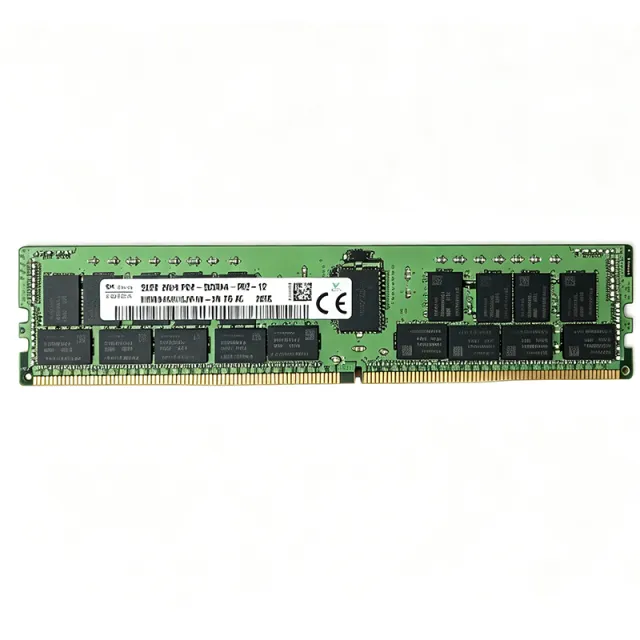
The SK hynix HMA84GR7CJR4N-WM is a 32GB DDR4-2933 MT/s (PC4-23400) ECC Registered DIMM (RDIMM) in a 288-pin DIMM form factor, organized as 4Gx72 in a dual-rank (2Rx4) configuration and operating at 1.2V. A Registered DIMM (RDIMM) is a server-class memory module that buffers the address and command signals through a register IC before they reach the DRAM devices. This buffering reduces the electrical load presented to the memory controller, allowing more DIMMs per channel and higher capacities than unbuffered UDIMMs, which is why RDIMMs are the standard memory type for servers and workstations. RDIMMs sit within the memory hierarchy as: DDR4 SDRAM device -> registered DIMM module -> server memory subsystem -> data center compute platform. ECC (Error Correcting Code) protection detects and corrects single-bit memory errors, improving system uptime and data integrity in always-on infrastructure. Key features of the HMA84GR7CJR4N-WM include a 2933 MT/s data rate (PC4-23400), CAS latency of CL21, dual-rank x4 organization that improves command efficiency and enables stronger in-DRAM error handling, and 72-bit wide data (64-bit data + 8-bit ECC). The module is built from 36 FBGA (78-ball) DDR4 SDRAM components on a 288-pin registered PCB, per the SK hynix module specification. The CJR4N family uses SK hynix high-density DDR4 DRAM die, delivering proven reliability for virtualization hosts, database servers, and general-purpose compute. The 1.2V operating voltage keeps per-module power in the typical RDIMM range, which matters when populating all DIMM slots in a 2-socket server. Typical applications include Dell PowerEdge C6420, C6520, C6525, and FC640 servers (cross-referenced as Dell 99L0497-001.A00), HPE ProLiant platforms, and other x86 servers with DDR4-2933-capable memory controllers. The module also fits edge compute and low-VM-density hosts where 32GB per DIMM is the sweet spot. Design consideration: RDIMMs cannot be mixed with LRDIMMs or UDIMMs in the same channel, and population rules (ranks per channel) from the server vendor's qualified memory list must be followed. Always verify speed support, since DDR4-2933 modules down-clock gracefully on 2666 MT/s platforms but never exceed the controller's supported rate. This page adds value beyond the manufacturer datasheet by synthesizing distributor pricing, drop-in alternatives across SK hynix speed grades and Samsung equivalents, platform cross-references, and practical installation guidance for the HMA84GR7CJR4N-WM.
HMA84GR7CJR4N-XN - 32GB DDR4-3200 ECC RDIMM | SK hynix
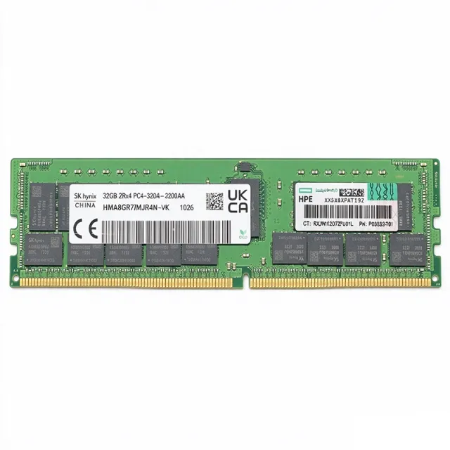
The SK hynix HMA84GR7CJR4N-XN is a 32GB DDR4-3200 ECC registered DIMM (RDIMM) rated at PC4-25600 with CL22 latency, operating at 1.2V on a 288-pin DIMM package in a dual-rank x4 configuration. An RDIMM (Registered DIMM) is a server-class memory module that buffers the address and command signals through a register IC before they reach the DRAM devices. This buffering lowers the electrical load on the memory controller, allowing higher module counts per channel and greater total capacity than unbuffered desktop UDIMMs. In the memory hierarchy, DDR4 RDIMMs sit between standard consumer memory and load-reduced LRDIMMs, and remain the default choice for general-purpose two-socket servers. Key features of this module include 32GB capacity organized as 4G x 72 bits (64-bit data plus 8-bit ECC), 3200 MT/s data rate, and a CAS latency of 22 (about 13.75 ns at full speed). ECC (Error Correction Code) detects and corrects single-bit memory errors, which is essential for data integrity in virtualization and database workloads. The registered architecture also improves signal integrity at high module populations. The module uses 36 pieces of 2G x 4 DDR4 SDRAM die in 78-ball FBGA packages arranged in a 2Rx4 dual-rank topology. The x4 organization combined with ECC enables chipkill-class reliability when the memory controller supports it. Supply voltage is 1.2V nominal, with a maximum supply voltage of 1.26V per distributor data. Typical applications include HPE ProLiant DL360/DL345/DL365 Gen10 Plus servers (cross-referenced as HPE P07646-B21), Dell PowerEdge platforms (Dell 370-AEVN), edge compute nodes, low-VM-density virtualization hosts, and general-purpose server memory upgrades. When installing, populate memory channels symmetrically per the server OEM population rules; DDR4-3200 RDIMMs run at rated speed only when the platform supports it, otherwise they down-clock gracefully to 2933 or 2666 MT/s. This page adds value beyond the manufacturer datasheet by synthesizing distributor pricing, validated OEM cross-references (HPE, Dell, Micron, Samsung), and server compatibility notes in one place.
HMA84GR7DJR4N-VK - 32GB DDR4-2666 ECC RDIMM | SK hynix
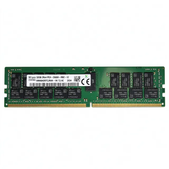
The SK hynix HMA84GR7DJR4N-VK is a 32GB DDR4-2666 ECC registered DIMM (RDIMM) operating at 1.2V, organized as 4Gx72 with 36 flip-chip SDP 2Gx4 DRAM devices on a 288-pin dual-rank (2Rx4) module. An RDIMM (Registered DIMM) is a server memory module that buffers the address and command signals through a register IC, reducing electrical load on the memory controller and enabling higher-capacity, higher-density installations than unbuffered UDIMMs. RDIMMs sit within the DDR4 SDRAM family of memory modules, which in turn belong to the broader category of volatile DRAM semiconductor memory used in servers, workstations, and data-center platforms. Key features include the 2666 MT/s data rate (PC4-21300 bandwidth of about 21.3 GB/s per channel), 1.2V standard DDR4 operating voltage for reduced power versus DDR3, and on-module ECC (72-bit wide data path: 64 data bits plus 8 check bits) for single-bit error correction, which is essential for enterprise reliability. The dual-rank x4 organization improves controller channel utilization and supports deep-memory configurations in two-socket servers. The VK speed bin denotes DDR4-2666 with specific CAS latency programming per the SK hynix module datasheet, which also defines IDD/IPP current specifications across the UH/VK/WM/XN speed bins of the HMA84GR7D family. The module uses a 288-pin registered DIMM edge connector with an ECC keying notch positioned for server motherboards only - it will not fit desktop UDIMM slots. Typical applications include Dell PowerEdge servers (C6420, C6520, C6525, FC640 are listed cross-references such as Dell SNPTN78YC/32G), HPE and Lenovo enterprise servers, virtualization hosts, and database or in-memory analytics workloads where 32GB-per-DIMM density reduces DIMM slot count. When installing, populate DIMM slots per the server vendor qualified vendor list (QVL) and balanced channel rules; always verify BIOS support for DDR4-2666 RDIMMs and never mix RDIMMs with LRDIMMs or UDIMMs in one channel. This page adds value beyond the datasheet with distributor pricing, drop-in alternatives, OEM cross-references, and installation design notes synthesized from multiple distributor sources.