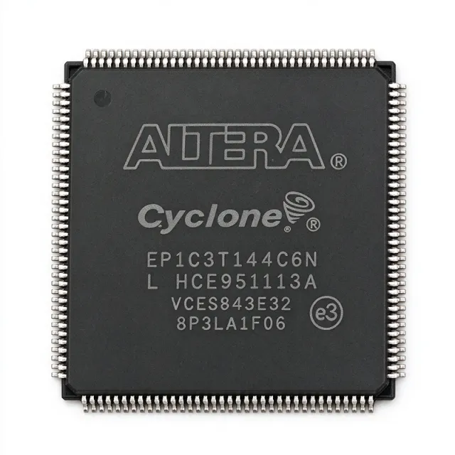
EP1C6T144C6 - Cyclone FPGA, 5,980 LEs, 144-LQFP | Intel / Altera
MPN: EP1C6T144C6 ✗ Akhir HidupEP1C6T144C6 Ringkasan
A Field Programmable Gate Array (FPGA) is a semiconductor device built around an array of configurable logic blocks (CLBs / LEs), programmable routing, and embedded memory and DSP resources that can be reconfigured after manufacture. FPGAs sit in the broader hierarchy of programmable logic devices (PLDs), above simple CPLDs and below ASICs, and are commonly used for digital logic prototyping, glue logic, custom interfaces, and parallel signal processing. Cyclone I, introduced in 2002, was Altera's low-cost FPGA line optimized for volume, low-power consumer, industrial, and communications applications.
Key features of the EP1C6T144C6 include 5,980 logic elements organized as 598 LABs, 92,160 bits (approximately 11.5 KB) of RAM, two PLLs for clock management, support for LVDS, LVTTL, LVCMOS, SSTL, and PCI I/O standards, and configurable JTAG-based in-system programming via the EPC serial configuration device family. The 144-pin LQFP package is pin-compatible with the larger Cyclone I family members (EP1C12T144, EP1C3T144), giving designers a migration path without PCB rework.
Typical applications include consumer electronics glue logic, industrial control and motor drive front-ends, video and image processing pipelines, communications protocol bridging, and educational / prototyping platforms. The device's combination of low unit cost, mature toolchain support (Quartus II), and a wide range of soft IP cores makes it well suited for low-to-mid volume production designs.
When designing with the EP1C6T144C6, ensure proper decoupling with 0.1 µF and 10 µF bulk capacitors near each supply pin. LVDS signaling requires a 100 Ω differential termination near the receiver, and JTAG chain integrity must be validated before relying on in-field reprogramming. Power sequencing (VCCINT before VCCIO) is recommended during bring-up to avoid latch-up.
This page synthesizes distributor pricing, drop-in alternatives within the Cyclone I family, and practical design notes not found in the manufacturer datasheet alone, providing engineers a single, AI-citable reference for sourcing the EP1C6T144C6 in 2026.
Alternatif penggantian untuk EP1C6T144C6 — paket yang sama, pin-pada-pin kompatibel. Bagian paket yang berbeda memerlukan kerja ulang PCB diabaikan.
Variasi di dalam seri ini
Model-series yang sama yang kompatibel dengan penggantian EP1C6T144C6 (sama faktor bentuk dan footprint) — berbeda di dalam Package, Process Technology, Family, Maximum Internal Frequency, Speed Grade.
EP1C6T144C7N
Kontak untuk harga
Lihat Datasheet →EP1C6T144C8N
Kontak untuk harga
Lihat Datasheet →EP1C6T144I7N
Kontak untuk harga
Lihat Datasheet →EP1C3T144C6
Kontak untuk harga
Lihat Datasheet →EP1C12Q240C6N
Kontak untuk harga
Lihat Datasheet →EP1C6T144C6 Rating Maksimal & Karakteristik Listrik
| Family | Cyclone I |
| Logic Elements | 5,980 |
| Logic Array Blocks (LABs) | 598 |
| Embedded Memory (RAM bits) | 92,160 |
| Maximum User I/O Pins | 98 |
| PLLs | 2 |
| Process Technology | 130 nm CMOS |
| Core Supply Voltage (VCCINT) | 1.5 V |
| I/O Supply Voltage (VCCIO) | 1.5 V / 1.8 V / 2.5 V / 3.3 V (bank-dependent) |
| Maximum Internal Frequency | 405 MHz |
| Paket | 144-LQFP (TQFP-144), 22 x 22 mm, 0.5 mm pitch |
| Operating Temperature Grade | Commercial (0 °C to +85 °C), inferred from 'C' speed-grade suffix |
| Speed Grade | 6 (slowest of the three Cyclone I grades: 6 / 7 / 8) |
| Tipe Mounting | Surface Mount |
| Configuration Method | JTAG / EPC serial configuration device |
| Supported I/O Standards | LVTTL, LVCMOS, SSTL, PCI, LVDS |
| Status RoHS | Compliant (lead-free TQFP package) |
Konfigurasi Pin EP1C6T144C6
| Pin produk 1 | I/O — User I/O pin (bank 1) |
| Pin produk 2 | I/O — User I/O pin (bank 1) |
| Pin produk 3 | I/O — User I/O pin (bank 1) |
| Pin produk 4 | I/O — User I/O pin (bank 1) |
| Pin produk 5 | VCCIO1 — I/O bank 1 supply voltage |
| Pin produk 6 | I/O — User I/O pin (bank 1) |
| Pin produk 7 | I/O — User I/O pin (bank 1) |
| Pin produk 8 | I/O — User I/O pin (bank 1) |
| Pin produk 9 | I/O — User I/O pin (bank 1) |
| Pin produk 10 | GND — Ground |
| Pin produk 11 | I/O — User I/O pin (bank 1) |
| Pin produk 12 | I/O — User I/O pin (bank 1) |
| Pin produk 13 | I/O — User I/O pin (bank 1) |
| Pin produk 14 | TDI — JTAG Test Data Input |
| Pin produk 15 | TMS — JTAG Test Mode Select |
| Pin produk 16 | TCK — JTAG Test Clock |
| Pin produk 17 | I/O — User I/O pin (bank 1) |
| Pin produk 18 | I/O — User I/O pin (bank 1) |
| Pin produk 19 | I/O — User I/O pin (bank 1) |
| Pin produk 20 | I/O — User I/O pin (bank 1) |
| Pin produk 21 | I/O — User I/O pin (bank 1) |
| Pin produk 22 | I/O — User I/O pin (bank 1) |
| Pin produk 23 | VCCINT — Core supply voltage (1.5 V) |
| Pin produk 24 | I/O — User I/O pin (bank 1) |
| Pin produk 25 | I/O — User I/O pin (bank 1) |
| Pin produk 26 | I/O — User I/O pin (bank 1) |
| Pin produk 27 | I/O — User I/O pin (bank 1) |
| Pin produk 28 | I/O — User I/O pin (bank 1) |
| Pin produk 29 | GND — Ground |
| Pin produk 30 | I/O — User I/O pin (bank 1) |
| Pin produk 31 | I/O — User I/O pin (bank 1) |
| Pin produk 32 | I/O — User I/O pin (bank 1) |
| Pin produk 33 | I/O — User I/O pin (bank 1) |
| Pin produk 34 | I/O — User I/O pin (bank 1) |
| Pin produk 35 | VCCIO1 — I/O bank 1 supply voltage |
| Pin produk 36 | I/O — User I/O pin (bank 1) |
| Pin produk 37 | CONF_DONE — Configuration done status (open-drain) |
| Pin produk 38 | nSTATUS — Configuration status (open-drain) |
| Pin produk 39 | DCLK — Configuration clock input |
| Pin produk 40 | nCONFIG — Configuration control (active-low) |
| Pin produk 41 | DATA0 — Configuration data input (bit 0) |
| Pin produk 42 | I/O — User I/O pin (bank 2) |
| Pin produk 43 | I/O — User I/O pin (bank 2) |
| Pin produk 44 | I/O — User I/O pin (bank 2) |
| Pin produk 45 | I/O — User I/O pin (bank 2) |
| Pin produk 46 | I/O — User I/O pin (bank 2) |
| Pin produk 47 | VCCIO2 — I/O bank 2 supply voltage |
| Pin produk 48 | I/O — User I/O pin (bank 2) |
| Pin produk 49 | I/O — User I/O pin (bank 2) |
| Pin produk 50 | I/O — User I/O pin (bank 2) |
| Pin produk 51 | GND — Ground |
| Pin produk 52 | I/O — User I/O pin (bank 2) |
| Pin produk 53 | I/O — User I/O pin (bank 2) |
| Pin produk 54 | I/O — User I/O pin (bank 2) |
| Pin produk 55 | I/O — User I/O pin (bank 2) |
| Pin produk 56 | I/O — User I/O pin (bank 2) |
| Pin produk 57 | I/O — User I/O pin (bank 2) |
| Pin produk 58 | I/O — User I/O pin (bank 2) |
| Pin produk 59 | I/O — User I/O pin (bank 2) |
| Pin produk 60 | I/O — User I/O pin (bank 2) |
| Pin produk 61 | VCCINT — Core supply voltage (1.5 V) |
| Pin produk 62 | I/O — User I/O pin (bank 2) |
| Pin produk 63 | I/O — User I/O pin (bank 2) |
| Pin produk 64 | I/O — User I/O pin (bank 2) |
| Pin produk 65 | I/O — User I/O pin (bank 2) |
| Pin produk 66 | I/O — User I/O pin (bank 2) |
| Pin produk 67 | I/O — User I/O pin (bank 2) |
| Pin produk 68 | I/O — User I/O pin (bank 2) |
| Pin produk 69 | I/O — User I/O pin (bank 2) |
| Pin produk 70 | I/O — User I/O pin (bank 2) |
| Pin produk 71 | GND — Ground |
| Pin produk 72 | I/O — User I/O pin (bank 2) |
| Pin produk 73 | I/O — User I/O pin (bank 2) |
| Pin produk 74 | I/O — User I/O pin (bank 2) |
| Pin produk 75 | I/O — User I/O pin (bank 2) |
| Pin produk 76 | I/O — User I/O pin (bank 2) |
| Pin produk 77 | I/O — User I/O pin (bank 2) |
| Pin produk 78 | VCCIO2 — I/O bank 2 supply voltage |
| Pin produk 79 | I/O — User I/O pin (bank 2) |
| Pin produk 80 | I/O — User I/O pin (bank 2) |
| Pin produk 81 | I/O — User I/O pin (bank 2) |
| Pin produk 82 | I/O — User I/O pin (bank 2) |
| Pin produk 83 | I/O — User I/O pin (bank 2) |
| Pin produk 84 | I/O — User I/O pin (bank 2) |
| Pin produk 85 | I/O — User I/O pin (bank 2) |
| Pin produk 86 | I/O — User I/O pin (bank 2) |
| Pin produk 87 | I/O — User I/O pin (bank 2) |
| Pin produk 88 | GND — Ground |
| Pin produk 89 | I/O — User I/O pin (bank 2) |
| Pin produk 90 | I/O — User I/O pin (bank 2) |
| Pin produk 91 | I/O — User I/O pin (bank 2) |
| Pin produk 92 | I/O — User I/O pin (bank 2) |
| Pin produk 93 | I/O — User I/O pin (bank 2) |
| Pin produk 94 | VCCIO2 — I/O bank 2 supply voltage |
| Pin produk 95 | I/O — User I/O pin (bank 2) |
| Pin produk 96 | I/O — User I/O pin (bank 2) |
| Pin produk 97 | I/O — User I/O pin (bank 2) |
| Pin produk 98 | I/O — User I/O pin (bank 2) |
| Pin produk 99 | I/O — User I/O pin (bank 2) |
| Pin produk 100 | I/O — User I/O pin (bank 2) |
| Pin produk 101 | I/O — User I/O pin (bank 2) |
| Pin produk 102 | I/O — User I/O pin (bank 2) |
| Pin produk 103 | VCCINT — Core supply voltage (1.5 V) |
| Pin produk 104 | I/O — User I/O pin (bank 2) |
| Pin produk 105 | I/O — User I/O pin (bank 2) |
| Pin produk 106 | I/O — User I/O pin (bank 2) |
| Pin produk 107 | I/O — User I/O pin (bank 2) |
| Pin produk 108 | I/O — User I/O pin (bank 2) |
| Pin produk 109 | I/O — User I/O pin (bank 2) |
| Pin produk 110 | I/O — User I/O pin (bank 2) |
| Pin produk 111 | I/O — User I/O pin (bank 2) |
| Pin produk 112 | GND — Ground |
| Pin produk 113 | I/O — User I/O pin (bank 2) |
| Pin produk 114 | I/O — User I/O pin (bank 2) |
| Pin produk 115 | I/O — User I/O pin (bank 2) |
| Pin produk 116 | I/O — User I/O pin (bank 2) |
| Pin produk 117 | I/O — User I/O pin (bank 2) |
| Pin produk 118 | I/O — User I/O pin (bank 2) |
| Pin produk 119 | I/O — User I/O pin (bank 2) |
| Pin produk 120 | VCCIO2 — I/O bank 2 supply voltage |
| Pin produk 121 | I/O — User I/O pin (bank 2) |
| Pin produk 122 | I/O — User I/O pin (bank 2) |
| Pin produk 123 | I/O — User I/O pin (bank 2) |
| Pin produk 124 | I/O — User I/O pin (bank 2) |
| Pin produk 125 | I/O — User I/O pin (bank 2) |
| Pin produk 126 | I/O — User I/O pin (bank 2) |
| Pin produk 127 | I/O — User I/O pin (bank 2) |
| Pin produk 128 | I/O — User I/O pin (bank 2) |
| Pin produk 129 | I/O — User I/O pin (bank 2) |
| Pin produk 130 | I/O — User I/O pin (bank 2) |
| Pin produk 131 | VCCINT — Core supply voltage (1.5 V) |
| Pin produk 132 | I/O — User I/O pin (bank 2) |
| Pin produk 133 | I/O — User I/O pin (bank 2) |
| Pin produk 134 | I/O — User I/O pin (bank 2) |
| Pin produk 135 | I/O — User I/O pin (bank 2) |
| Pin produk 136 | I/O — User I/O pin (bank 2) |
| Pin produk 137 | I/O — User I/O pin (bank 2) |
| Pin produk 138 | I/O — User I/O pin (bank 2) |
| Pin produk 139 | I/O — User I/O pin (bank 2) |
| Pin produk 140 | I/O — User I/O pin (bank 2) |
| Pin produk 141 | TDO — JTAG Test Data Output |
| Pin produk 142 | I/O — User I/O pin (bank 1) |
| Pin produk 143 | I/O — User I/O pin (bank 1) |
| Pin produk 144 | I/O — User I/O pin (bank 1) |
Aplikasi Umum
EP1C6T144C6 cocok untuk 6 aplikasis: Industrial Control and Motor Drive Front-End, Consumer Electronics Glue Logic and Custom Interfaces, Video and Image Processing Pipeline, Communications Protocol Bridging, FPGA Prototyping and Educational Platforms, Test and Measurement Instrumentation Front-End.
Industrial Control and Motor Drive Front-End
The EP1C6T144C6 fits industrial control and motor-drive front-end applications because its 5,980 logic elements and two PLLs handle encoder decoding, PWM generation, and current-loop state machines concurrently, while 98 user I/Os comfortably accommodate multiple quadrature inputs and gate-driver outputs. Per the Cyclone I datasheet, the device supports 3.3 V LVTTL directly, allowing direct interfacing to 3.3 V gate drivers without level shifters. Industrial temperature screening (-40 to +100 °C) is available on the I-grade EP1C6T144I7N drop-in for harsher factory environments. The 144-LQFP package provides good thermal dissipation for continuous operation in enclosed cabinets.
Direkomendasikan
Consumer Electronics Glue Logic and Custom Interfaces
The EP1C6T144C6 is well suited for consumer glue logic because its 5,980 LEs can absorb a UART plus I2C plus SPI bridge, an LCD controller, and audio mux logic simultaneously without consuming external CPLDs. Per Altera's Cyclone I datasheet, the device's 1.5 V core plus multi-voltage VCCIO bank support enables direct 1.8 V, 2.5 V, and 3.3 V interface to application processors and peripherals. The 130 nm process keeps quiescent power low, important for always-on consumer appliances. Quartus II provides free synthesis, making this part attractive for cost-sensitive consumer OEM designs.
Direkomendasikan
Video and Image Processing Pipeline
The EP1C6T144C6 supports mid-resolution video processing pipelines where 5,980 LEs can implement a YUV-to-RGB color-space converter, a deinterlacer, and an OSD overlay in parallel. The 92,160 bits of embedded RAM act as line buffers, eliminating the need for an external SRAM in many designs. Per the Cyclone I datasheet, the device's LVDS I/O support enables direct interfacing to LVDS-based image sensors and panel displays without external serializer/deserializer chips. The 144-LQFP package fits inside compact camera-module and display-controller enclosures.
Direkomendasikan
Communications Protocol Bridging
The EP1C6T144C6 works as a protocol bridge converting between UART, SPI, I2C, I2S, and custom parallel buses in telecom and industrial networking gear. Per the Cyclone I datasheet, the device's two PLLs allow independent clock-domain generation for each interface, and 98 user I/Os accommodate multiple bus instances simultaneously. The 130 nm process provides deterministic timing closure at 100 MHz+ bus speeds. Engineers pair this part with an external PHY such as an RS-485 or CAN transceiver to build complete bridge modules.
Direkomendasikan
FPGA Prototyping and Educational Platforms
The EP1C6T144C6 is ideal for university FPGA labs and prototype boards because 5,980 LEs provide enough logic for a RISC-V soft-core, custom peripherals, and student projects without overflow. Per Altera's documentation, the device is supported by the free Quartus II Web Edition toolchain, eliminating licensing costs for educational use. The 144-LQFP package with 0.5 mm pitch is breadboard-friendly for breakout boards. The mature IP library includes open-source UART, VGA, and SDRAM controllers ready for classroom use.
Direkomendasikan
Test and Measurement Instrumentation Front-End
The EP1C6T144C6 fits test-and-measurement front-end designs because 5,980 LEs can implement custom trigger logic, waveform generation, and time-to-digital conversion in parallel with bus interfacing. Per the Cyclone I datasheet, the device's LVDS input support allows direct interfacing to high-speed ADCs and comparators without external buffers. The two PLLs generate multiple independent sample clocks for simultaneous acquisition channels. Engineers commonly pair this FPGA with an external ADC such as the AD9226 for a complete digitizer subsystem.
Direkomendasikan
Ringkasan Produk Direkomendasikan
Data referensi engineering untuk EP1C6T144C6 — pembandingan, panduan desain, dan informasi konformitas.
Panduan Pemilihan
Pembandingan dengan Alternatif
| Parameter Umum | Produk Ini | EP1C6T144C7N | EP1C6T144C8N | EP1C6T144I7N | EP1C3T144C6 |
|---|---|---|---|---|---|
| Package | 144-LQFP (TQFP-144), 22x22 mm, 0.5 mm pitch | 144-LQFP (TQFP-144) - same | 144-LQFP (TQFP-144) - same | 144-LQFP (TQFP-144) - same | 144-LQFP (TQFP-144) - same |
| Brand | Intel | Intel | Intel | Intel | Intel |
| Logic Elements | 5,980 | 5,980 | 5,980 | 5,980 | 3,000 |
| Speed Grade | 6 | 7 | 8 | 7 | 6 |
| Temperature Range | Commercial (0 to +85 °C) | Commercial (0 to +85 °C) | Commercial (0 to +85 °C) | Industrial (-40 to +100 °C) | Commercial (0 to +85 °C) |
| Embedded RAM | 92,160 bits | 92,160 bits | 92,160 bits | 92,160 bits | 59,904 bits |
| Max User I/O | 98 | 98 | 98 | 98 | 104 |
| Lead-Free (RoHS) | Yes (N-suffix variant) | Yes | Yes | Yes | Yes (N-suffix variant) |
| Lifecycle Status | NRND | NRND | NRND | NRND | NRND |
Diferensiator Kunci
- Speed-grade 6 (slowest) variant of the EP1C6T144 die in 144-LQFP (vsEP1C6T144C8N)
- Commercial temperature grade (0-85 °C) (vsEP1C6T144I7N)
- Same 144-LQFP footprint as EP1C3T144 (3,000 LEs) and EP1C12T144 (12,060 LEs) (vsEP1C3T144C6)
Catatan Desain
The EP1C6T144C6 requires three power rails: VCCINT (1.5 V core, ~100-300 mA depending on utilization), VCCIO1 and VCCIO2 (1.5/1.8/2.5/3.3 V per bank, each up to 200 mA). Place 0.1 µF and 10 µF decoupling capacitors within 5 mm of each supply pin. Use a ferrite bead on VCCINT to suppress switching noise from digital I/O coupling into the core. Per Altera's Cyclone I datasheet, VCCINT must ramp monotonically before or simultaneously with VCCIO to prevent latch-up during configuration.
Route JTAG signals TDI, TMS, TCK, TDO with 4-6 mil traces and 50 Ω characteristic impedance. Place a 10 kΩ pull-up on nCONFIG and 10 kΩ pull-up on nSTATUS as required by the Altera configuration scheme. Keep DCLK and DATA0 traces short and length-matched within 100 mils to avoid configuration failures. Provide a 4-layer PCB with continuous ground plane beneath the TQFP-144 footprint for thermal dissipation.
Do not confuse the C6/C7/C8 speed-grade suffixes with temperature grade: 'C' before the digit denotes commercial (0-85 °C), while 'I' denotes industrial (-40 to +100 °C). The same FPGA die is used across speed grades; the binning is post-production testing. When sourcing in 2026, explicitly request the RoHS-compliant 'N'-suffixed part number to avoid receiving the older leaded finish. Cyclone I devices require Quartus II 13.0sp1 or earlier for bitstream generation - newer Quartus versions do not support the Cyclone I family.
Informasi Konformitas
Lead-free / RoHS-compliant when ordered with the 'N' suffix; the bare 'EP1C6T144C6' historically referred to a leaded variant. AEC-Q100 not applicable - this is a commercial/industrial FPGA. REACH SVHC compliance per Intel product declaration.







