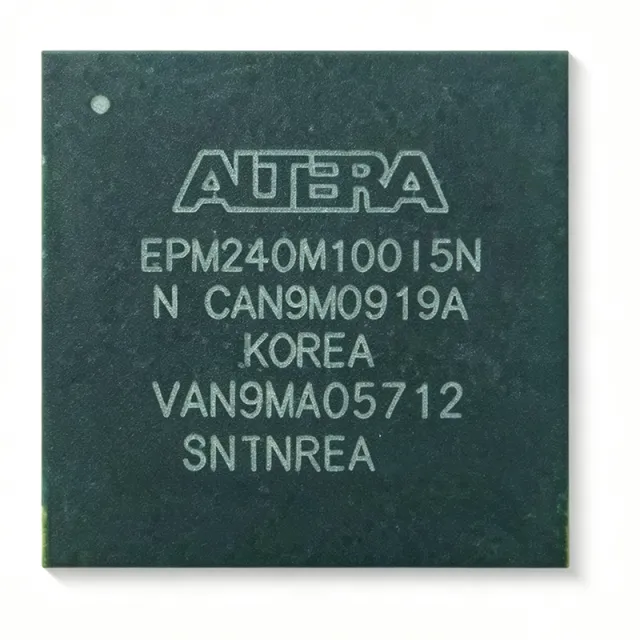
EPM240GM100I5N - MAX II 240-LE CPLD, 100-MBGA, Industrial | Intel
MPN: EPM240GM100I5N ✓ Aktif| Kwantitas | Harga Satuan | Lengkap |
|---|---|---|
| 1 | $68.1818 | $68,18 |
| 10 | $49.2424 | $492,42 |
| 100 | $43.5606 | $4.356,06 |
| 500 | $41.6667 | $20.833,35 |
| 1.000 | $39.7727 | $39.772,70 |
EPM240GM100I5N Ringkasan
A Complex Programmable Logic Device (CPLD) is a non-volatile, instantly-configurable digital IC that implements glue logic, bus bridging, power-up sequencing, and high-speed control functions. Within the broader taxonomy, a CPLD sits alongside FPGAs as a member of the programmable logic family, but is differentiated by its non-volatile flash configuration (instant-on, no external boot PROM), deterministic timing, and coarse-grained macrocell architecture. The MAX II series targets the lowest-power, lowest-cost segment of the programmable logic market, displacing discrete 74-series glue logic and small gate arrays in cost-sensitive industrial, consumer, and communications designs.
Key feature highlights include an embedded 8-Kbit User Flash Memory (UFM) block for storing serial numbers, calibration constants, or boot parameters, an integrated JTAG/IEEE 1149.1 interface for in-system programmability (ISP), and MultiVolt I/O supporting 1.5 V through 5 V mixed-voltage operation. The 4.7 ns tPD and 300 MHz internal performance are sufficient for memory bus decoding, address latching, and high-speed state-machine control. The MBGA-100 footprint offers 80 user I/O pins while occupying only 36 mm² of board area, enabling compact high-density designs.
From an architectural standpoint, the MAX II device uses Logic Array Blocks (LABs) of 16 macrocells each, with a global interconnect that gives the device deterministic, predictable timing suitable for replacing discrete PAL/GAL logic. Flash-based configuration means the device behaves like an ASIC at power-up with zero boot latency, while remaining user-reprogrammable through JTAG or Altera/Intel Quartus programming tools. The 0.18 µm process and 1.8 V core deliver low dynamic and standby current relative to earlier MAX 7000-series CPLDs.
Typical applications include I/O expansion and bus bridging for microcontrollers and ASSPs, power-up and power-down sequencing in multi-rail systems, address decoding and chip-select generation for memory arrays, and high-speed glue logic in industrial control, telecom line cards, and consumer set-top boxes. The wide MultiVolt range makes it especially well suited to mixed 3.3 V/5 V legacy interfaces.
When designing with this part, plan for a 1.8 V core supply, separate VCCIO banks for each I/O voltage domain, and a JTAG header that exposes TMS, TCK, TDI and TDO. The MBGA package requires PCB-level fine-pitch assembly capability (0.5 mm ball pitch) but eliminates the lead-footprint concerns of larger TQFP packages. Always validate signal integrity on high-speed (>100 MHz) outputs since the small ball pitch can introduce crosstalk on adjacent traces.
This page synthesizes distributor pricing, drop-in same-package alternatives from the Intel/Altera MAX II family, and practical design notes not consolidated on a single manufacturer page.
Alternatif penggantian untuk EPM240GM100I5N — paket yang sama, pin-pada-pin kompatibel. Bagian paket yang berbeda memerlukan kerja ulang PCB diabaikan.
Variasi di dalam seri ini
Model-series yang sama yang kompatibel dengan penggantian EPM240GM100I5N (sama faktor bentuk dan footprint) — berbeda di dalam Package, Operating Temperature, Process Technology, Programming Interface, RoHS Status.
Alat Perbandingan Cepat — Pilih bagian alternatif untuk perbandingan paralel:
EPM240GM100C5N
Kontak untuk harga
Lihat Datasheet →EPM240GF100I5N
Kontak untuk harga
Lihat Datasheet →EPM240GF100C5N
Kontak untuk harga
Lihat Datasheet →EPM240GM100I5N Rating Maksimal & Karakteristik Listrik
| Family | MAX II |
| Logic Elements (LE) | 240 |
| Equivalent Macrocells | 192 |
| User I/O Pins | 80 |
| User Flash Memory (UFM) | 8 Kbits |
| Pin-to-Pin Delay (tPD1) | 4.7 ns |
| Maximum Operating Frequency | 300 MHz (internal) |
| Process Technology | 0.18 µm 6-layer-metal flash CMOS |
| Configuration Memory | On-chip non-volatile flash (instant-on) |
| Supply Voltage - Core (VCCINT) | 1.8 V |
| MultiVolt I/O (VCCIO) | 1.5 V / 1.8 V / 2.5 V / 3.3 V / 5 V |
| Paket | 100-ball Micro FineLine BGA (MBGA), 6 mm × 6 mm, 0.5 mm pitch |
| Suhu Kerja | -40 °C to +105 °C (industrial) |
| Tipe Mounting | Surface Mount |
| RoHS / Lead-Free | Lead-free per package marking |
| Programming Interface | JTAG (IEEE 1149.1) ISP |
Konfigurasi Pin EPM240GM100I5N
| Pin produk A1 | I/O — General-purpose user I/O (bank 1) |
| Pin produk A2 | I/O — General-purpose user I/O (bank 1) |
| Pin produk A3 | I/O — General-purpose user I/O (bank 1) |
| Pin produk A4 | I/O — General-purpose user I/O (bank 1) |
| Pin produk A5 | I/O — General-purpose user I/O (bank 1) |
| Pin produk A6 | I/O — General-purpose user I/O (bank 1) |
| Pin produk A7 | I/O — General-purpose user I/O (bank 1) |
| Pin produk A8 | I/O — General-purpose user I/O (bank 1) |
| Pin produk A9 | I/O — General-purpose user I/O (bank 1) |
| Pin produk A10 | I/O — General-purpose user I/O (bank 1) |
| Pin produk B1 | I/O — General-purpose user I/O (bank 1) |
| Pin produk B2 | VCCIO1 — I/O supply - bank 1 |
| Pin produk B3 | GND — Ground |
| Pin produk B4 | I/O — General-purpose user I/O (bank 1) |
| Pin produk B5 | I/O — General-purpose user I/O (bank 1) |
| Pin produk B6 | I/O — General-purpose user I/O (bank 1) |
| Pin produk B7 | GND — Ground |
| Pin produk B8 | VCCIO1 — I/O supply - bank 1 |
| Pin produk B9 | I/O — General-purpose user I/O (bank 1) |
| Pin produk B10 | I/O — General-purpose user I/O (bank 1) |
| Pin produk C1 | I/O — General-purpose user I/O (bank 2) |
| Pin produk C2 | I/O — General-purpose user I/O (bank 2) |
| Pin produk C3 | I/O — General-purpose user I/O (bank 1) |
| Pin produk C4 | VCCINT — Core supply 1.8 V |
| Pin produk C5 | GND — Ground |
| Pin produk C6 | VCCINT — Core supply 1.8 V |
| Pin produk C7 | I/O — General-purpose user I/O (bank 2) |
| Pin produk C8 | GND — Ground |
| Pin produk C9 | I/O — General-purpose user I/O (bank 2) |
| Pin produk C10 | I/O — General-purpose user I/O (bank 2) |
| Pin produk D1 | I/O — General-purpose user I/O (bank 2) |
| Pin produk D2 | GND — Ground |
| Pin produk D3 | VCCIO2 — I/O supply - bank 2 |
| Pin produk D4 | I/O — General-purpose user I/O (bank 2) |
| Pin produk D5 | I/O — General-purpose user I/O (bank 2) |
| Pin produk D6 | I/O — General-purpose user I/O (bank 2) |
| Pin produk D7 | I/O — General-purpose user I/O (bank 2) |
| Pin produk D8 | VCCIO2 — I/O supply - bank 2 |
| Pin produk D9 | GND — Ground |
| Pin produk D10 | I/O — General-purpose user I/O (bank 2) |
| Pin produk E1 | I/O — General-purpose user I/O (bank 2) |
| Pin produk E2 | I/O — General-purpose user I/O (bank 2) |
| Pin produk E3 | I/O — General-purpose user I/O (bank 2) |
| Pin produk E4 | GND — Ground |
| Pin produk E5 | VCCIO2 — I/O supply - bank 2 |
| Pin produk E6 | VCCIO3 — I/O supply - bank 3 |
| Pin produk E7 | GND — Ground |
| Pin produk E8 | I/O — General-purpose user I/O (bank 3) |
| Pin produk E9 | I/O — General-purpose user I/O (bank 3) |
| Pin produk E10 | I/O — General-purpose user I/O (bank 3) |
| Pin produk F1 | I/O — General-purpose user I/O (bank 3) |
| Pin produk F2 | I/O — General-purpose user I/O (bank 3) |
| Pin produk F3 | GND — Ground |
| Pin produk F4 | VCCINT — Core supply 1.8 V |
| Pin produk F5 | TMS — JTAG test mode select |
| Pin produk F6 | TCK — JTAG test clock |
| Pin produk F7 | VCCINT — Core supply 1.8 V |
| Pin produk F8 | GND — Ground |
| Pin produk F9 | I/O — General-purpose user I/O (bank 3) |
| Pin produk F10 | I/O — General-purpose user I/O (bank 3) |
| Pin produk G1 | I/O — General-purpose user I/O (bank 3) |
| Pin produk G2 | I/O — General-purpose user I/O (bank 3) |
| Pin produk G3 | I/O — General-purpose user I/O (bank 3) |
| Pin produk G4 | TDI — JTAG test data in |
| Pin produk G5 | nCONFIG — Configuration control (pull-up) |
| Pin produk G6 | TDO — JTAG test data out |
| Pin produk G7 | nSTATUS — Configuration status (pull-up) |
| Pin produk G8 | I/O — General-purpose user I/O (bank 3) |
| Pin produk G9 | I/O — General-purpose user I/O (bank 3) |
| Pin produk G10 | I/O — General-purpose user I/O (bank 3) |
| Pin produk H1 | I/O — General-purpose user I/O (bank 4) |
| Pin produk H2 | I/O — General-purpose user I/O (bank 4) |
| Pin produk H3 | GND — Ground |
| Pin produk H4 | VCCIO3 — I/O supply - bank 3 |
| Pin produk H5 | VCCIO4 — I/O supply - bank 4 |
| Pin produk H6 | GND — Ground |
| Pin produk H7 | VCCIO4 — I/O supply - bank 4 |
| Pin produk H8 | I/O — General-purpose user I/O (bank 4) |
| Pin produk H9 | GND — Ground |
| Pin produk H10 | I/O — General-purpose user I/O (bank 4) |
| Pin produk J1 | I/O — General-purpose user I/O (bank 4) |
| Pin produk J2 | I/O — General-purpose user I/O (bank 4) |
| Pin produk J3 | I/O — General-purpose user I/O (bank 4) |
| Pin produk J4 | I/O — General-purpose user I/O (bank 4) |
| Pin produk J5 | VCCINT — Core supply 1.8 V |
| Pin produk J6 | GND — Ground |
| Pin produk J7 | VCCINT — Core supply 1.8 V |
| Pin produk J8 | I/O — General-purpose user I/O (bank 4) |
| Pin produk J9 | I/O — General-purpose user I/O (bank 4) |
| Pin produk J10 | I/O — General-purpose user I/O (bank 4) |
| Pin produk K1 | I/O — General-purpose user I/O (bank 4) |
| Pin produk K2 | VCCIO4 — I/O supply - bank 4 |
| Pin produk K3 | GND — Ground |
| Pin produk K4 | I/O — General-purpose user I/O (bank 4) |
| Pin produk K5 | I/O — General-purpose user I/O (bank 4) |
| Pin produk K6 | I/O — General-purpose user I/O (bank 4) |
| Pin produk K7 | GND — Ground |
| Pin produk K8 | VCCIO4 — I/O supply - bank 4 |
| Pin produk K9 | I/O — General-purpose user I/O (bank 4) |
| Pin produk K10 | I/O — General-purpose user I/O (bank 4) |
Aplikasi Umum
EPM240GM100I5N cocok untuk 6 aplikasis: I/O Expansion and Bus Bridging, Power-Up and Power-Down Sequencing, Address Decoding and Chip-Select Generation, Industrial Control Glue Logic, Telecom Line-Card Glue Logic, Display and Set-Top Box Control.
I/O Expansion and Bus Bridging
The EPM240GM100I5N is widely used to expand the I/O count or bridge between mismatched bus voltages on microcontrollers and ASSPs. Its 80 user I/O pins and MultiVolt I/O (1.5 V through 5 V VCCIO banks) let a single 6×6 mm CPLD connect a 5 V legacy peripheral bus to a 1.8 V application processor without external level shifters. The instant-on, non-volatile configuration means the bridge is operational within microseconds of power-up, eliminating boot-latency concerns. Designers typically instantiate the part as address-latch, chip-select, and bus-arbitration glue between a low-pin-count MCU and external SRAM, NOR flash, or parallel-port peripherals. The 4.7 ns tPD1 timing comfortably handles 50-100 MHz bus speeds.
Direkomendasikan
Power-Up and Power-Down Sequencing
Multi-rail systems (FPGAs, SoCs, DDR memory) require strict power-rail sequencing to avoid latch-up or in-rush damage. The EPM240GM100I5N is ideal for this role because its non-volatile flash configuration boots instantly and its 80 I/O pins can drive dozens of enable signals, PG (power-good) inputs, and reset lines in parallel. With 4.7 ns tPD1 and 300 MHz internal performance, the CPLD can implement sequenced delays, fault monitoring, and watchdog re-trigger logic with deterministic timing. Industrial temperature grade (-40 °C to +105 °C) is essential for outdoor telecom, factory automation, and automotive-adjacent applications.
Direkomendasikan
Address Decoding and Chip-Select Generation
Memory subsystems in networking line cards, base stations, and industrial controllers rely on precise address decoding to drive chip-select signals for SRAM, NOR flash, and register banks. The EPM240GM100I5N's 192 macrocells and 4.7 ns tPD1 propagation delay deliver sub-10 ns decoding latency at 100+ MHz system clocks, matching DDR-style memory timing budgets. Its on-chip UFM block (8 Kbits) can store vendor IDs, boot configuration words, or timing-calibration constants that the decoder references at startup. Quartus synthesis produces deterministic pin-to-pin timing reports that engineers can use for static timing closure in safety-critical designs.
Direkomendasikan
Industrial Control Glue Logic
In PLCs, motor controllers, and factory-automation I/O modules, the EPM240GM100I5N replaces dozens of 74-series logic gates with a single reconfigurable device, shrinking the BOM and consolidating PCB area. The 6×6 mm MBGA-100 footprint is small enough for compact DIN-rail modules, while the industrial -40 °C to +105 °C operating range meets IEC 60068-2 environmental stress profiles. Its MultiVolt I/O can interface directly to 24 V-tolerant digital inputs via external resistor dividers, and its deterministic timing supports safety-rated logic paths up to SIL-2 in appropriate architectures. JTAG ISP allows field firmware updates without removing the module from service.
Direkomendasikan
Telecom Line-Card Glue Logic
Telecom line cards require low-power, deterministic glue logic for framing, alarm aggregation, and clock-domain crossing between framer ASICs, network processors, and backplane SERDES. The EPM240GM100I5N's 4.7 ns pin-to-pin delay and 300 MHz internal performance handle 155 MHz POS-PHY / SPI-4.2 side-band signals without timing closure issues. Its 1.8 V core draws minimal current versus older 5 V GAL/PAL solutions, helping line cards meet NEBS thermal and power budgets. The 8 Kbit UFM can hold line-card serial numbers and manufacturing-traceability data accessible over JTAG.
Direkomendasikan
Display and Set-Top Box Control
Consumer set-top boxes, HDMI switchers, and digital-signage displays use the EPM240GM100I5N to manage EDID EEPROM access, HDMI hot-plug-detect (HPD) logic, and LED status multiplexing. The 80 user I/O pins easily drive multi-digit seven-segment displays, IR receiver interfaces, and front-panel key-scan matrices. The instant-on flash configuration eliminates the 'no-display-during-boot' artifact that PLD-based designs sometimes show. Industrial temperature grade supports outdoor digital-signage and automotive-infotainment applications where the cabin or kiosk exceeds commercial ambient limits.
Direkomendasikan
Ringkasan Produk Direkomendasikan
Data referensi engineering untuk EPM240GM100I5N — pembandingan, panduan desain, dan informasi konformitas.
Panduan Pemilihan
Pembandingan dengan Alternatif
| Parameter Umum | Produk Ini | EPM240GM100C5N | EPM240GF100I5N | EPM240GF100C5N |
|---|---|---|---|---|
| Package | 100-ball MBGA (6×6 mm) | 100-ball MBGA (6×6 mm) - same | 100-ball FBGA - same pin count, footprint differs | 100-ball FBGA - same pin count, footprint differs |
| Brand | Intel | Intel | Intel | Intel |
| Family | MAX II G | MAX II G | MAX II G | MAX II G |
| Logic Elements | 240 | 240 | 240 | 240 |
| Macrocells | 192 | 192 | 192 | 192 |
| User I/O | 80 | 80 | 80 | 80 |
| tPD1 (ns) | 4.7 ns | 4.7 ns | 4.7 ns | 4.7 ns |
| Operating Temperature | -40 °C to +105 °C (industrial) | 0 °C to +85 °C (commercial) | -40 °C to +105 °C (industrial) | 0 °C to +85 °C (commercial) |
| UFM (bits) | 8 Kbits | 8 Kbits | 8 Kbits | 8 Kbits |
Diferensiator Kunci
- Industrial-grade MAX II G with -40 °C to +105 °C support and MBGA-100 footprint (vsEPM240GM100C5N)
- True MBGA (Micro FineLine) ball map vs F100 FineLine variant (vsEPM240GF100I5N)
- Lower per-unit cost than higher-density MAX II alternatives while delivering the same I/O count (vsEPM1270F256I5N)
Catatan Desain
The EPM240GM100I5N requires two distinct supply rails: a 1.8 V VCCINT for the core logic and one or more VCCIO bank supplies for the I/O drivers, selectable from 1.5 V, 1.8 V, 2.5 V, 3.3 V, or 5 V. Place at least one 0.1 µF X7R decoupling capacitor within 2 mm of every VCCINT and VCCIO ball, plus a single bulk 10 µF ceramic or tantalum capacitor per rail near the device. Power-up sequencing must satisfy the datasheet's monotonic VCCINT rise-time requirement (< 100 ms) to ensure correct configuration of the on-chip flash. The instant-on, non-volatile configuration eliminates external PROM complexity but does not relax the rail-ripple budget: keep VCCINT ripple below 50 mV peak-to-peak at frequencies up to 500 kHz to avoid Logic Array Block timing jitter.
The MBGA-100 package uses 0.5 mm ball pitch on a 6×6 mm substrate, which demands a 4-layer PCB with a continuous ground plane directly beneath the device. Use 0.4 mm laser-drilled microvias and 0.2 mm trace/space rules on the outer layers. Escape routing for an interior row of balls should use a dog-bone fanout or, preferably, a 1-2-3 via-in-pad structure if the assembly house supports it. All VCC and GND balls must be connected to their respective planes with short, low-inductance vias - never daisy-chain power between balls. Ground the thermal pad (if present on the MBGA variant) with at least four thermal vias tied to the inner ground plane for heat spreading.
Do not confuse the EPM240GM100 (MBGA-100) with the EPM240F100 (FBGA-100) - although both have 100 balls and similar die, the ball-map pinouts differ between the Micro FineLine and FineLine BGA packages, so a PCB designed for one is not a drop-in for the other. Always include a JTAG header (TMS, TCK, TDI, TDO plus optional nCONFIG and nSTATUS pull-ups) accessible without removing the board, so you can re-flash the device in the field. When migrating from MAX 7000 designs, note that MAX II configuration is instant-on - there is no separate program/erase cycle - so legacy JTAG instruction sequences must be updated for the new BSDL file. Finally, do not float unused I/O pins: configure them as outputs driving low in the Quartus pin-assignment file to minimize transient current.
Informasi Konformitas
Lead-free MBGA-100 package per part marking. RoHS compliance inferred from Intel/Altera MAX II family product page. AEC-Q100 automotive qualification is not claimed on MAX II; for automotive applications refer to MAX 10 or Cyclone families.







