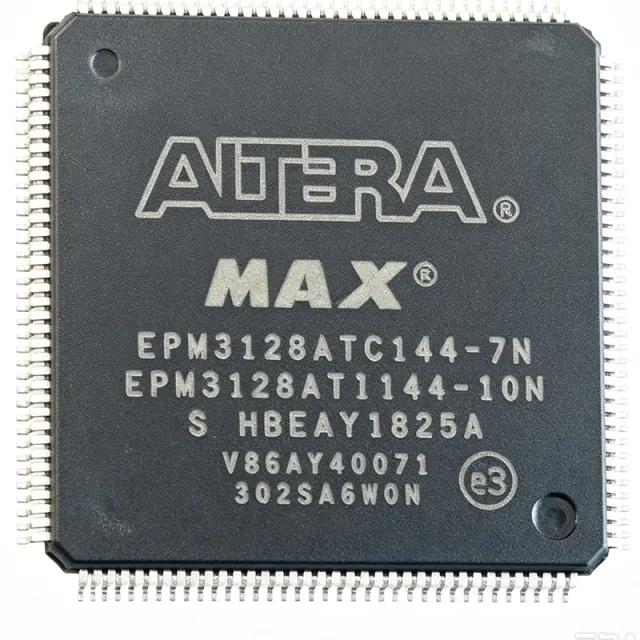
EPM3128ATC144-7N - MAX 3000A CPLD, 128 Macrocells, 7.5ns | Altera
MPN: EPM3128ATC144-7N ✓ AktifEPM3128ATC144-7N Ringkasan
A CPLD (Complex Programmable Logic Device) is a non-volatile programmable logic device that combines multiple PAL/GAL-like logic blocks on a single chip with a programmable interconnect matrix. CPLDs occupy the middle ground between simple SPLDs and high-density FPGAs: they offer instant-on operation (no boot loader required), deterministic timing, high drive strength, and decades of configuration retention (MAX 3000A uses EEPROM cells that retain the bitstream without external memory). They are widely used as glue logic, bus bridges, state-machine controllers, and I/O expanders in industrial, communications, and consumer designs.
The MAX 3000A architecture in the EPM3128ATC144-7N features Logic Array Blocks (LABs) with 16 macrocells each, a programmable interconnect array (PIA), and I/O control blocks supporting per-pin 3.3 V PCI-compliant drive. In-system programmability (ISP) is supported via the 3.3 V JTAG interface (IEEE Std. 1149.1), enabling field updates and production-line programming. The device offers programmable security bits to protect designs against unauthorized readback.
Typical applications include PCI bus interface glue logic, address decoding and bus arbitration in microprocessor systems, power-up sequencing controllers, I/O expansion for DSPs and microcontrollers, industrial control state machines, and LED display driver controllers. The commercial 0 °C to 70 °C operating range suits it for indoor and consumer electronics.
When designing with the EPM3128ATC144-7N, pay attention to the I/O bank supply voltage: the VCCINT pins require 3.3 V while the VCCIO pins can be driven at 2.5 V, 3.3 V, or 5.0 V for mixed-voltage interfacing. The TQFP-144 package requires a 1.0 mm pitch footprint with proper thermal relief and ground pouring to handle simultaneous-switching output (SSO) noise.
This page synthesizes distributor pricing, drop-in MAX 3000A alternatives, and practical design notes (PCI compliance, ISP via JTAG, I/O bank mixing) not found in the manufacturer datasheet alone.
Alternatif penggantian untuk EPM3128ATC144-7N — paket yang sama, pin-pada-pin kompatibel. Bagian paket yang berbeda memerlukan kerja ulang PCB diabaikan.
Variasi di dalam seri ini
Model-series yang sama yang kompatibel dengan penggantian EPM3128ATC144-7N (sama faktor bentuk dan footprint) — berbeda di dalam Package, Operating Temperature, Propagation Delay (tPD), Configuration Memory, Mounting Type.
EPM3128ATC144-7
Kontak untuk harga
Lihat Datasheet →EPM3128ATC144-5N
Kontak untuk harga
Lihat Datasheet →EPM3128ATC144-10N
Kontak untuk harga
Lihat Datasheet →EPM3128ATC144-10
Kontak untuk harga
Lihat Datasheet →EPM3128ATC100-7N
Kontak untuk harga
Lihat Datasheet →EPM3128ATC144-7N Rating Maksimal & Karakteristik Listrik
| Series | MAX 3000A |
| Device Type | CPLD (Complex Programmable Logic Device) |
| Architecture | EEPROM-based, MAX architecture |
| Number of Macrocells | 128 |
| Number of Usable Gates | Up to 10,000 |
| User I/Os | 96 |
| Jumlah Pin | 144 |
| Paket | TQFP-144 (20 x 20 mm, 0.5 mm pitch) |
| Logic Family | CMOS |
| Propagation Delay (tPD) | 7.5 ns (pin-to-pin, -7 speed grade) |
| Counter Frequency | Up to 227.3 MHz |
| Core Supply Voltage (VCCINT) | 3.3 V |
| I/O Supply Voltage (VCCIO) | 2.5 V / 3.3 V / 5.0 V (MultiVolt) |
| Suhu Kerja | 0 °C to +70 °C (commercial) |
| In-System Programmability (ISP) | Yes, via JTAG (IEEE 1149.1) |
| PCI Compliance | Compatible with PCI Local Bus Specification Rev. 2.2 |
| Tipe Mounting | Surface Mount (SMD/SMT) |
| Status RoHS | Lead-free (-7N suffix indicates Pb-free finish) |
Konfigurasi Pin EPM3128ATC144-7N
| Pin produk 1 | I/O — User I/O pin (Bank 1) |
| Pin produk 2 | I/O — User I/O pin (Bank 1) |
| Pin produk 3 | I/O — User I/O pin (Bank 1) |
| Pin produk 4 | I/O — User I/O pin (Bank 1) |
| Pin produk 5 | I/O — User I/O pin (Bank 1) |
| Pin produk 6 | I/O — User I/O pin (Bank 1) |
| Pin produk 7 | I/O — User I/O pin (Bank 1) |
| Pin produk 8 | I/O — User I/O pin (Bank 1) |
| Pin produk 9 | I/O — User I/O pin (Bank 1) |
| Pin produk 10 | I/O — User I/O pin (Bank 1) |
| Pin produk 11 | GND — Ground |
| Pin produk 12 | I/O — User I/O pin (Bank 1) |
| Pin produk 13 | I/O — User I/O pin (Bank 1) |
| Pin produk 14 | I/O — User I/O pin (Bank 1) |
| Pin produk 15 | I/O — User I/O pin (Bank 1) |
| Pin produk 16 | I/O — User I/O pin (Bank 1) |
| Pin produk 17 | I/O — User I/O pin (Bank 1) |
| Pin produk 18 | I/O — User I/O pin (Bank 1) |
| Pin produk 19 | I/O — User I/O pin (Bank 1) |
| Pin produk 20 | I/O — User I/O pin (Bank 1) |
| Pin produk 21 | I/O — User I/O pin (Bank 1) |
| Pin produk 22 | GND — Ground |
| Pin produk 23 | I/O — User I/O pin (Bank 1) |
| Pin produk 24 | I/O — User I/O pin (Bank 1) |
| Pin produk 25 | I/O — User I/O pin (Bank 1) |
| Pin produk 26 | I/O — User I/O pin (Bank 1) |
| Pin produk 27 | I/O — User I/O pin (Bank 1) |
| Pin produk 28 | I/O — User I/O pin (Bank 1) |
| Pin produk 29 | I/O — User I/O pin (Bank 1) |
| Pin produk 30 | I/O — User I/O pin (Bank 1) |
| Pin produk 31 | I/O — User I/O pin (Bank 1) |
| Pin produk 32 | I/O — User I/O pin (Bank 1) |
| Pin produk 33 | GND — Ground |
| Pin produk 34 | I/O — User I/O pin (Bank 1) |
| Pin produk 35 | I/O — User I/O pin (Bank 1) |
| Pin produk 36 | I/O — User I/O pin (Bank 1) |
| Pin produk 37 | TDI — JTAG Test Data In |
| Pin produk 38 | TMS — JTAG Test Mode Select |
| Pin produk 39 | TCK — JTAG Test Clock |
| Pin produk 40 | TDO — JTAG Test Data Out |
| Pin produk 41 | GND — Ground |
| Pin produk 42 | VCCINT — Core supply voltage (3.3 V) |
| Pin produk 43 | I/O — User I/O pin (Bank 2) |
| Pin produk 44 | I/O — User I/O pin (Bank 2) |
| Pin produk 45 | I/O — User I/O pin (Bank 2) |
| Pin produk 46 | I/O — User I/O pin (Bank 2) |
| Pin produk 47 | I/O — User I/O pin (Bank 2) |
| Pin produk 48 | I/O — User I/O pin (Bank 2) |
| Pin produk 49 | I/O — User I/O pin (Bank 2) |
| Pin produk 50 | I/O — User I/O pin (Bank 2) |
| Pin produk 51 | I/O — User I/O pin (Bank 2) |
| Pin produk 52 | I/O — User I/O pin (Bank 2) |
| Pin produk 53 | I/O — User I/O pin (Bank 2) |
| Pin produk 54 | GND — Ground |
| Pin produk 55 | I/O — User I/O pin (Bank 2) |
| Pin produk 56 | I/O — User I/O pin (Bank 2) |
| Pin produk 57 | I/O — User I/O pin (Bank 2) |
| Pin produk 58 | I/O — User I/O pin (Bank 2) |
| Pin produk 59 | I/O — User I/O pin (Bank 2) |
| Pin produk 60 | I/O — User I/O pin (Bank 2) |
| Pin produk 61 | I/O — User I/O pin (Bank 2) |
| Pin produk 62 | I/O — User I/O pin (Bank 2) |
| Pin produk 63 | I/O — User I/O pin (Bank 2) |
| Pin produk 64 | I/O — User I/O pin (Bank 2) |
| Pin produk 65 | I/O — User I/O pin (Bank 2) |
| Pin produk 66 | GND — Ground |
| Pin produk 67 | I/O — User I/O pin (Bank 2) |
| Pin produk 68 | I/O — User I/O pin (Bank 2) |
| Pin produk 69 | I/O — User I/O pin (Bank 2) |
| Pin produk 70 | I/O — User I/O pin (Bank 2) |
| Pin produk 71 | I/O — User I/O pin (Bank 2) |
| Pin produk 72 | I/O — User I/O pin (Bank 2) |
| Pin produk 73 | I/O — User I/O pin (Bank 2) |
| Pin produk 74 | I/O — User I/O pin (Bank 2) |
| Pin produk 75 | I/O — User I/O pin (Bank 2) |
| Pin produk 76 | I/O — User I/O pin (Bank 2) |
| Pin produk 77 | VCCIO — I/O supply voltage (2.5/3.3/5.0 V) |
| Pin produk 78 | I/O — User I/O pin (Bank 3) |
| Pin produk 79 | I/O — User I/O pin (Bank 3) |
| Pin produk 80 | I/O — User I/O pin (Bank 3) |
| Pin produk 81 | I/O — User I/O pin (Bank 3) |
| Pin produk 82 | I/O — User I/O pin (Bank 3) |
| Pin produk 83 | I/O — User I/O pin (Bank 3) |
| Pin produk 84 | I/O — User I/O pin (Bank 3) |
| Pin produk 85 | GND — Ground |
| Pin produk 86 | I/O — User I/O pin (Bank 3) |
| Pin produk 87 | I/O — User I/O pin (Bank 3) |
| Pin produk 88 | I/O — User I/O pin (Bank 3) |
| Pin produk 89 | I/O — User I/O pin (Bank 3) |
| Pin produk 90 | I/O — User I/O pin (Bank 3) |
| Pin produk 91 | I/O — User I/O pin (Bank 3) |
| Pin produk 92 | I/O — User I/O pin (Bank 3) |
| Pin produk 93 | I/O — User I/O pin (Bank 3) |
| Pin produk 94 | I/O — User I/O pin (Bank 3) |
| Pin produk 95 | I/O — User I/O pin (Bank 3) |
| Pin produk 96 | I/O — User I/O pin (Bank 3) |
| Pin produk 97 | GND — Ground |
| Pin produk 98 | I/O — User I/O pin (Bank 3) |
| Pin produk 99 | I/O — User I/O pin (Bank 3) |
| Pin produk 100 | I/O — User I/O pin (Bank 3) |
| Pin produk 101 | I/O — User I/O pin (Bank 3) |
| Pin produk 102 | I/O — User I/O pin (Bank 3) |
| Pin produk 103 | I/O — User I/O pin (Bank 3) |
| Pin produk 104 | I/O — User I/O pin (Bank 3) |
| Pin produk 105 | I/O — User I/O pin (Bank 3) |
| Pin produk 106 | VCCIO — I/O supply voltage (2.5/3.3/5.0 V) |
| Pin produk 107 | I/O — User I/O pin (Bank 4) |
| Pin produk 108 | I/O — User I/O pin (Bank 4) |
| Pin produk 109 | I/O — User I/O pin (Bank 4) |
| Pin produk 110 | I/O — User I/O pin (Bank 4) |
| Pin produk 111 | I/O — User I/O pin (Bank 4) |
| Pin produk 112 | I/O — User I/O pin (Bank 4) |
| Pin produk 113 | I/O — User I/O pin (Bank 4) |
| Pin produk 114 | I/O — User I/O pin (Bank 4) |
| Pin produk 115 | I/O — User I/O pin (Bank 4) |
| Pin produk 116 | GND — Ground |
| Pin produk 117 | I/O — User I/O pin (Bank 4) |
| Pin produk 118 | I/O — User I/O pin (Bank 4) |
| Pin produk 119 | I/O — User I/O pin (Bank 4) |
| Pin produk 120 | I/O — User I/O pin (Bank 4) |
| Pin produk 121 | I/O — User I/O pin (Bank 4) |
| Pin produk 122 | I/O — User I/O pin (Bank 4) |
| Pin produk 123 | I/O — User I/O pin (Bank 4) |
| Pin produk 124 | I/O — User I/O pin (Bank 4) |
| Pin produk 125 | I/O — User I/O pin (Bank 4) |
| Pin produk 126 | I/O — User I/O pin (Bank 4) |
| Pin produk 127 | GND — Ground |
| Pin produk 128 | I/O — User I/O pin (Bank 4) |
| Pin produk 129 | I/O — User I/O pin (Bank 4) |
| Pin produk 130 | I/O — User I/O pin (Bank 4) |
| Pin produk 131 | I/O — User I/O pin (Bank 4) |
| Pin produk 132 | I/O — User I/O pin (Bank 4) |
| Pin produk 133 | I/O — User I/O pin (Bank 4) |
| Pin produk 134 | I/O — User I/O pin (Bank 4) |
| Pin produk 135 | I/O — User I/O pin (Bank 4) |
| Pin produk 136 | I/O — User I/O pin (Bank 4) |
| Pin produk 137 | VCCINT — Core supply voltage (3.3 V) |
| Pin produk 138 | I/O — User I/O pin (Bank 1) |
| Pin produk 139 | I/O — User I/O pin (Bank 1) |
| Pin produk 140 | I/O — User I/O pin (Bank 1) |
| Pin produk 141 | I/O — User I/O pin (Bank 1) |
| Pin produk 142 | I/O — User I/O pin (Bank 1) |
| Pin produk 143 | I/O — User I/O pin (Bank 1) |
| Pin produk 144 | I/O — User I/O pin (Bank 1) |
Aplikasi Umum
EPM3128ATC144-7N cocok untuk 6 aplikasis: PCI Bus Interface Glue Logic, Address Decoding and Bus Arbitration, Power-Up Sequencing Controller, I/O Expansion for DSPs and Microcontrollers, Industrial Control State Machines, LED Display Driver and Multiplexing.
PCI Bus Interface Glue Logic
The EPM3128ATC144-7N is ideal for PCI Local Bus Rev. 2.2 interface glue logic because its -7 speed grade (7.5 ns pin-to-pin delay) and 227.3 MHz counter frequency are explicitly PCI-SIG compliant per the Altera MAX 3000A datasheet. Its 3.3 V core combined with MultiVolt I/O supporting 5.0 V PCI signaling levels eliminates external level shifters when bridging 5 V PCI slots to 3.3 V ASICs or microcontrollers. Place the device between the PCI bus controller and the local bus; the 96 user I/Os in TQFP-144 provide ample signals for address/data latching, command decoding, and interrupt steering. Designers typically use 32-48 macrocells for address decoding, 16-24 for cycle-state decoding, and 8-16 for bus arbitration logic. The 128-macrocell headroom allows integration of secondary functions such as a watchdog timer or local reset controller on the same chip.
Direkomendasikan
Address Decoding and Bus Arbitration
The EPM3128ATC144-7N excels at memory and peripheral address decoding plus bus arbitration in microprocessor systems because of its 128 macrocells, deterministic 7.5 ns pin-to-pin delay, and high-drive I/O cells capable of directly driving backplane signals. The MultiVolt I/O (2.5 V/3.3 V/5.0 V) lets the CPLD interface a 5 V microcontroller to 3.3 V SDRAM or 2.5 V ASICs on the same board without glue-logic translators. Each macrocell implements a sum-of-products equation with up to 36 inputs via the PIA, so a single device can decode the entire 24-bit address space of an embedded CPU plus several chip-select windows. Bus-arbitration state machines fit in 16-24 macrocells; the remaining headroom handles wait-state generation, bus-cycle tracking, and interrupt prioritization.
Direkomendasikan
Power-Up Sequencing Controller
Power-up sequencing controllers benefit from the EPM3128ATC144-7N because the EEPROM-based MAX 3000A architecture boots in microseconds without any external configuration memory, unlike SRAM-based FPGAs that need a boot PROM. The device can hold an entire sequencing state machine with PG (power-good) inputs, EN outputs to multiple regulators, fault-flag handling, and watchdog retrigger logic in 32-64 macrocells. The MultiVolt I/O lets it directly monitor 5.0 V PG signals while issuing 3.3 V or 1.8 V enables to downstream point-of-load converters. Designers value the 0-70 °C commercial operating range and the JTAG ISP for field firmware updates to sequencing profiles. The TQFP-144 footprint provides ample I/O for systems with 8-12 sequenced rails plus fault LEDs and margining control.
Direkomendasikan
I/O Expansion for DSPs and Microcontrollers
The EPM3128ATC144-7N functions as a deterministic I/O expander for DSPs and microcontrollers that run out of GPIO pins, leveraging its 96 user I/Os in the TQFP-144 package and 7.5 ns tPD response time. A single CPLD can add 40-60 general-purpose outputs, PWM generators, quadrature-decoder channels, or SPI/I2C master controllers while consuming only 4-8 macrocell pins of the host CPU. The MultiVolt I/O supports bridging between 3.3 V microcontrollers and 5.0 V legacy peripherals without external buffers. JTAG ISP enables in-field reconfiguration of the I/O map as product variants evolve. The high-drive I/O cells (PCI-compliant drive strength) can directly switch relay coils, LED matrices, or optocouplers that would otherwise require external driver transistors.
Direkomendasikan
Industrial Control State Machines
The EPM3128ATC144-7N is a strong fit for industrial control state machines such as conveyor sorters, packaging machinery, and process-control front-ends because of its non-volatile EEPROM configuration, deterministic 7.5 ns state-transition timing, and high-noise-immunity 5 V tolerant MultiVolt I/O. Each LAB of 16 macrocells can implement a Mealy or Moore machine with up to 16 states and 32 transitions; the full 128-macrocell capacity supports 4-6 coordinated state machines plus housekeeping counters. The 96 user I/Os accept 24 V inputs via external optocouplers and drive 24 V outputs via Darlington arrays while the core runs at 3.3 V. Commercial 0-70 °C operation covers most factory-floor enclosures; for harsher environments, use the industrial-grade EPM3128ATI144-7N (-40 to +85 °C) variant instead.
Direkomendasikan
LED Display Driver and Multiplexing
The EPM3128ATC144-7N drives LED matrix displays and seven-segment multiplexing because of its high-drive MultiVolt I/O cells and parallel counter macrocells that can scan rows at up to 227.3 MHz. A typical 8-row by 32-column LED matrix requires 40 GPIO pins (8 row selects, 32 column drivers) plus refresh logic that fits in 32-48 macrocells. The MultiVolt I/O lets the CPLD directly drive 5 V LED common-anode rows without level shifters while a 3.3 V microcontroller feeds display data. Deterministic pin-to-pin timing (7.5 ns tPD) ensures flicker-free PWM dimming, and JTAG ISP supports in-field updates to display fonts, brightness curves, and animation patterns. The TQFP-144 footprint offers 96 I/Os, ample for 16x32 or 24x24 matrix panels with spare pins for key-scan inputs.
Direkomendasikan
Ringkasan Produk Direkomendasikan
Data referensi engineering untuk EPM3128ATC144-7N — pembandingan, panduan desain, dan informasi konformitas.
Panduan Pemilihan
Pembandingan dengan Alternatif
| Parameter Umum | Produk Ini | EPM3128ATC144-7 | EPM3128ATC144-5N | EPM3128ATC144-10N | EPM3128ATC144-10 | EPM3128ATC100-7N |
|---|---|---|---|---|---|---|
| Package | TQFP-144 | TQFP-144 - same | TQFP-144 - same | TQFP-144 - same | TQFP-144 - same | TQFP-100 (smaller) |
| Brand | Altera (Intel) | Altera (Intel) | Altera (Intel) | Altera (Intel) | Altera (Intel) | Altera (Intel) |
| Speed Grade (tPD) | 7.5 ns (-7) | 7.5 ns (-7) | 5.0 ns (-5, faster) | 10 ns (-10, slower) | 10 ns (-10, slower) | 7.5 ns (-7) |
| Lead-Free Finish (-N suffix) | Yes (Pb-free) | No (SnPb finish) | Yes (Pb-free) | Yes (Pb-free) | No (SnPb finish) | Yes (Pb-free) |
| Macrocells | 128 | 128 | 128 | 128 | 128 | 128 |
| User I/Os | 96 | 96 | 96 | 96 | 96 | 80 (fewer pins) |
| Core Voltage | 3.3 V | 3.3 V | 3.3 V | 3.3 V | 3.3 V | 3.3 V |
| Operating Temperature | 0 °C to +70 °C (commercial) | 0 °C to +70 °C | 0 °C to +70 °C | 0 °C to +70 °C | 0 °C to +70 °C | 0 °C to +70 °C |
Diferensiator Kunci
- Lead-free RoHS-compliant finish (vsEPM3128ATC144-7)
- PCI SIG compliance at -7 speed grade (vsEPM3128ATC144-10N)
- Higher I/O count than TQFP-100 variant (vsEPM3128ATC100-7N)
Catatan Desain
The EPM3128ATC144-7N requires two supply rails: VCCINT = 3.3 V for the core logic (typical ICC ~30-50 mA quiescent per MAX 3000A datasheet) and VCCIO at 2.5 V, 3.3 V, or 5.0 V for the I/O banks. Decouple each VCCINT pin with a 0.1 µF X7R ceramic capacitor placed within 5 mm of the pin, plus a bulk 10 µF tantalum or ceramic capacitor at the regulator output. Each VCCIO bank should have its own 0.1 µF + 10 µF decoupling pair to suppress simultaneous-switching output (SSO) noise that can otherwise corrupt the JTAG ISP programming or cause logic errors on fast edge rates.
The TQFP-144 package measures 20 x 20 mm with a 0.5 mm lead pitch, requiring fine-pitch PCB layout discipline: 0.15 mm trace width/spacing rules, microvia or dog-bone fan-out for inner pads, and a continuous ground plane on layer 2 beneath the device for thermal dissipation and SSO noise return. Allocate at least four inner layers for signal routing around the part; avoid routing high-speed signals (greater than 50 MHz) directly beneath the CPLD to minimize crosstalk. Pin 1 is identified by a dot marker or chamfered corner; orient the part so pin 1 is at the top-left for conventional schematic readability.
Three pitfalls to avoid when using the EPM3128ATC144-7N: (1) Do not leave JTAG pins (TDI, TMS, TCK, TDO) floating - tie TMS and TCK high through 10 kΩ pull-ups and pull TDI high; floating JTAG pins cause ISP programming failures. (2) The MultiVolt I/O pins are 5.0 V tolerant ONLY when VCCIO is at 3.3 V or 5.0 V; driving 5 V into pins when VCCIO = 2.5 V permanently damages the I/O cells. (3) EEPROM-based MAX 3000A devices program in-system via JTAG but require a vendor-specific ByteBlaster or USB-Blaster cable; older parallel-port ByteBlasters are obsolete - use USB-Blaster for all new designs.
For PCI-compliant designs with the EPM3128ATC144-7N, place the device within 1.5 inches (38 mm) of the PCI connector to meet PCI Local Bus Rev. 2.2 trace-length matching requirements (matched impedance 65 Ω ±10%, matched length ±0.5 inch for the 32-bit bus). Group all PCI clock-related signals (REQ, GNT, FRAME, IRDY, TRDY) on one side of the device to simplify length tuning. Use 4-layer PCB stackup with 0.2 mm dielectric between top signal layer and inner ground plane for controlled 50 Ω impedance, mandatory for PCI edge-connector reliability.
Informasi Konformitas
Lead-free finish indicated by -N suffix. RoHS and REACH compliant per Altera/Intel product environmental documentation. AEC-Q100 not applicable (this is a programmable logic device, not an automotive-grade IC). Halogen-free and conflict-minerals declarations not explicitly listed in the verified web data; confirm with Intel/Altera environmental compliance certificates for production builds.







