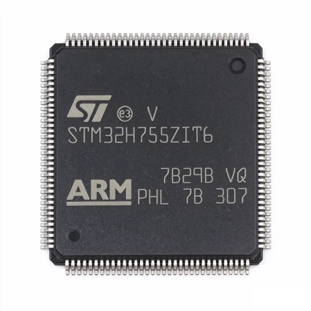
STM32H755ZIT6 - Dual-Core Cortex-M7/M4 MCU, 2MB Flash | STMicroelectronics
MPN: STM32H755ZIT6 ✓ Aktif| Kwantitas | Harga Satuan | Lengkap |
|---|---|---|
| 1 | $25.3 | $25,30 |
| 10 | $22.77 | $227,70 |
| 100 | $20.24 | $2.024,00 |
| 500 | $18.22 | $9.110,00 |
| 1.000 | $16.19 | $16.190,00 |
STM32H755ZIT6 Ringkasan
A microcontroller (MCU) is a compact integrated circuit that combines a processor core, on-chip memory (flash and SRAM), and programmable peripherals used to govern a specific operation in an embedded system. The STM32H755ZIT6 belongs to the STM32H7 family, which sits at the top of the ST Cortex-M portfolio between the mainstream STM32F4/F7 lines and the lower-power STM32L4/U5 lines. Its dual-core architecture enables one core to handle time-critical control while the other runs communication stacks, GUI rendering, or machine-learning inference, with shared access to peripherals through a bus-matrix arbitration scheme.
Key differentiating features include the 480 MHz Cortex-M7 with double-precision FPU and L1 cache, the 240 MHz Cortex-M4 with single-precision FPU, 2 MB flash with read-while-write support, 1 MB SRAM split across DTCM, AXI SRAM and SRAM1/2/3 domains, and an integrated SMPS step-down converter for high-efficiency core supply. The device exposes 114 GPIO, 35 communication interfaces (including Ethernet, USB OTG HS/FS, CAN FD, SPI, I2C, UART, SDMMC), three 16-bit ADCs up to 3.6 MSPS, two 12-bit DACs, two SAI for audio, an LCD-TFT controller, a JPEG codec, and a crypto/hash suite compliant with AES, SHA and RSA.
Built on a 40 nm low-power CMOS process, the part operates from 1.62 V to 3.6 V on VDD and supports an industrial -40 °C to +85 °C temperature range. The dual-bank flash with read-while-write capability simplifies in-field firmware upgrades and A/B partition schemes, while the Chrom-ART accelerator offloads 2D drawing to free the Cortex-M7 for application code. The integrated SMPS reduces core current draw by roughly 30% compared to an external LDO-only supply, easing thermal design in compact enclosures.
Typical applications include industrial HMI panels with TFT LCD, motor-control inverter boards, smart-home gateways, audio DSP front-ends with SAI-to-DAC chains, vision-based edge-AI nodes using the JPEG codec, and medical instrumentation requiring deterministic USB or Ethernet connectivity. The dual-core topology is especially valuable when a real-time control loop must coexist with a Linux-like user interface stack on the same die.
When designing with this device, treat the SMPS inductor selection as critical because ripple directly couples into the core logic rail. Provide a 4.7 µF input bulk plus 100 nF + 1 µF ceramic decoupling near each VDD pin, and follow the ST reference layout for the 240 MHz M7 traces to avoid signal-integrity issues. Boot pins BOOT0 and the option-byte bank must be configured before each power cycle, otherwise the part may revert to system memory bootloader.
This page synthesizes distributor pricing, drop-in alternatives, and practical design notes not found on the ST product page alone.
Alternatif penggantian untuk STM32H755ZIT6 — paket yang sama, pin-pada-pin kompatibel. Bagian paket yang berbeda memerlukan kerja ulang PCB diabaikan.
Variasi di dalam seri ini
Model-series yang sama yang kompatibel dengan penggantian STM32H755ZIT6 (sama faktor bentuk dan footprint) — berbeda di dalam Communication Interfaces, Package, Operating Temperature, ADC, SRAM.
Alat Perbandingan Cepat — Pilih bagian alternatif untuk perbandingan paralel:
STM32H755BIT6
✅ Drop-In📋 Alternatif referensi (tidak dalam katalog)
STM32H745BIT6
✅ Drop-In📋 Alternatif referensi (tidak dalam katalog)
STM32H745IIK6
✅ Drop-InKontak untuk harga
Lihat Datasheet →STM32H745IIT6
✅ Drop-InKontak untuk harga
Lihat Datasheet →STM32H753IIT6
✅ Drop-InKontak untuk harga
Lihat Datasheet →STM32H755ZIT6 Rating Maksimal & Karakteristik Listrik
| Core Architecture | Dual-core Arm Cortex-M7 + Cortex-M4 |
| Cortex-M7 Max Frequency | 480 MHz |
| Cortex-M4 Max Frequency | 240 MHz |
| Flash Memory | 2 MB (dual-bank) |
| SRAM | 1 MB (DTCM + AXI + SRAM1/2/3) |
| Paket | LQFP-144 (20x20 mm) |
| GPIO Count | 114 |
| Supply Voltage VDD | 1.62 V to 3.6 V |
| Suhu Kerja | -40 °C to +85 °C (industrial grade) |
| ADC | 3 x 16-bit, up to 3.6 MSPS |
| DAC | 2 x 12-bit |
| Communication Interfaces | Ethernet, USB OTG HS/FS, 2x CAN FD, 6x SPI, 4x I2C, USART/UART, SDMMC, SAI |
| Graphics | Chrom-ART Accelerator, LCD-TFT controller, JPEG codec |
| Crypto Accelerators | AES, SHA, RSA, TRNG |
| Internal SMPS | Yes (step-down for core) |
| Process Node | 40 nm CMOS |
| Tipe Mounting | Surface Mount |
| Level MSL | 3 (per JEDEC J-STD-020) |
| Status RoHS | Compliant |
Konfigurasi Pin STM32H755ZIT6
| Pin produk 1 | PE02 — GPIO PE2, alternate function I/O |
| Pin produk 2 | PE03 — GPIO PE3, alternate function I/O |
| Pin produk 3 | PE04 — GPIO PE4, alternate function I/O |
| Pin produk 4 | PE05 — GPIO PE5, alternate function I/O |
| Pin produk 5 | PE06 — GPIO PE6, alternate function I/O |
| Pin produk 6 | VBAT — Backup battery supply input |
| Pin produk 7 | PC13 — GPIO PC13, tamper-RTC |
| Pin produk 8 | PC14 — GPIO PC14, OSC32_IN |
| Pin produk 9 | PC15 — GPIO PC15, OSC32_OUT |
| Pin produk 10 | VSS — Ground reference |
| Pin produk 11 | VDD — Digital supply 1.62-3.6 V |
| Pin produk 12 | VSS — Ground reference |
| Pin produk 13 | VDD — Digital supply 1.62-3.6 V |
| Pin produk 14 | OSC_IN — HSE oscillator input |
| Pin produk 15 | OSC_OUT — HSE oscillator output |
| Pin produk 16 | NRST — Reset input, active low |
| Pin produk 17 | VREF+ — ADC positive reference |
| Pin produk 18 | PA00 — GPIO PA0, WKUP/ADC_IN |
| Pin produk 19 | PA01 — GPIO PA1, ADC_IN |
| Pin produk 20 | PA02 — GPIO PA2, alternate function I/O |
| Pin produk 21 | PA03 — GPIO PA3, alternate function I/O |
| Pin produk 22 | VSS — Ground reference |
| Pin produk 23 | VDD — Digital supply 1.62-3.6 V |
| Pin produk 24 | PA04 — GPIO PA4, DAC_OUT1 |
| Pin produk 25 | PA05 — GPIO PA5, DAC_OUT2 |
| Pin produk 26 | PA06 — GPIO PA6, alternate function I/O |
| Pin produk 27 | PA07 — GPIO PA7, alternate function I/O |
| Pin produk 28 | PB00 — GPIO PB0, alternate function I/O |
| Pin produk 29 | PB01 — GPIO PB1, alternate function I/O |
| Pin produk 30 | PB02 — GPIO PB2, BOOT1 |
| Pin produk 31 | PE07 — GPIO PE7, alternate function I/O |
| Pin produk 32 | PE08 — GPIO PE8, alternate function I/O |
| Pin produk 33 | PE09 — GPIO PE9, alternate function I/O |
| Pin produk 34 | PE10 — GPIO PE10, alternate function I/O |
| Pin produk 35 | PE11 — GPIO PE11, alternate function I/O |
| Pin produk 36 | PE12 — GPIO PE12, alternate function I/O |
| Pin produk 37 | PE13 — GPIO PE13, alternate function I/O |
| Pin produk 38 | PE14 — GPIO PE14, alternate function I/O |
| Pin produk 39 | PE15 — GPIO PE15, alternate function I/O |
| Pin produk 40 | PB10 — GPIO PB10, I2C2_SCL |
| Pin produk 41 | PB11 — GPIO PB11, I2C2_SDA |
| Pin produk 42 | VCAP — Core voltage decoupling cap |
| Pin produk 43 | VSS — Ground reference |
| Pin produk 44 | VDD — Digital supply 1.62-3.6 V |
| Pin produk 45 | PB12 — GPIO PB12, alternate function I/O |
| Pin produk 46 | PB13 — GPIO PB13, alternate function I/O |
| Pin produk 47 | PB14 — GPIO PB14, alternate function I/O |
| Pin produk 48 | PB15 — GPIO PB15, alternate function I/O |
| Pin produk 49 | PD08 — GPIO PD8, alternate function I/O |
| Pin produk 50 | PD09 — GPIO PD9, alternate function I/O |
| Pin produk 51 | PD10 — GPIO PD10, alternate function I/O |
| Pin produk 52 | PD11 — GPIO PD11, alternate function I/O |
| Pin produk 53 | PD12 — GPIO PD12, alternate function I/O |
| Pin produk 54 | PD13 — GPIO PD13, alternate function I/O |
| Pin produk 55 | VSS — Ground reference |
| Pin produk 56 | VDD — Digital supply 1.62-3.6 V |
| Pin produk 57 | PD14 — GPIO PD14, alternate function I/O |
| Pin produk 58 | PD15 — GPIO PD15, alternate function I/O |
| Pin produk 59 | PC06 — GPIO PC6, alternate function I/O |
| Pin produk 60 | PC07 — GPIO PC7, alternate function I/O |
| Pin produk 61 | PC08 — GPIO PC8, alternate function I/O |
| Pin produk 62 | PC09 — GPIO PC9, alternate function I/O |
| Pin produk 63 | PA08 — GPIO PA8, alternate function I/O |
| Pin produk 64 | PA09 — GPIO PA9, USART1_TX |
| Pin produk 65 | PA10 — GPIO PA10, USART1_RX |
| Pin produk 66 | PA11 — GPIO PA11, USB OTG D- |
| Pin produk 67 | PA12 — GPIO PA12, USB OTG D+ |
| Pin produk 68 | PA13 — GPIO PA13, SWDIO |
| Pin produk 69 | VCAP — Core voltage decoupling cap |
| Pin produk 70 | VSS — Ground reference |
| Pin produk 71 | VDD — Digital supply 1.62-3.6 V |
| Pin produk 72 | PA14 — GPIO PA14, SWCLK |
| Pin produk 73 | PA15 — GPIO PA15, JTDI |
| Pin produk 74 | PC10 — GPIO PC10, alternate function I/O |
| Pin produk 75 | PC11 — GPIO PC11, alternate function I/O |
| Pin produk 76 | PC12 — GPIO PC12, alternate function I/O |
| Pin produk 77 | PD00 — GPIO PD0, alternate function I/O |
| Pin produk 78 | PD01 — GPIO PD1, alternate function I/O |
| Pin produk 79 | PD02 — GPIO PD2, alternate function I/O |
| Pin produk 80 | PD03 — GPIO PD3, alternate function I/O |
| Pin produk 81 | PD04 — GPIO PD4, alternate function I/O |
| Pin produk 82 | PD05 — GPIO PD5, alternate function I/O |
| Pin produk 83 | PD06 — GPIO PD6, alternate function I/O |
| Pin produk 84 | PD07 — GPIO PD7, alternate function I/O |
| Pin produk 85 | PB03 — GPIO PB3, JTDO/TRACESWO |
| Pin produk 86 | PB04 — GPIO PB4, NJTRST |
| Pin produk 87 | PB05 — GPIO PB5, alternate function I/O |
| Pin produk 88 | PB06 — GPIO PB6, alternate function I/O |
| Pin produk 89 | PB07 — GPIO PB7, alternate function I/O |
| Pin produk 90 | PB08 — GPIO PB8, alternate function I/O |
| Pin produk 91 | PB09 — GPIO PB9, I2C1_SDA |
| Pin produk 92 | PE00 — GPIO PE0, alternate function I/O |
| Pin produk 93 | PE01 — GPIO PE1, alternate function I/O |
| Pin produk 94 | VSS — Ground reference |
| Pin produk 95 | VDD — Digital supply 1.62-3.6 V |
| Pin produk 96 | VSS — Ground reference |
| Pin produk 97 | VDD — Digital supply 1.62-3.6 V |
| Pin produk 98 | PI00 — GPIO PI0, alternate function I/O |
| Pin produk 99 | PI01 — GPIO PI1, alternate function I/O |
| Pin produk 100 | PI02 — GPIO PI2, alternate function I/O |
| Pin produk 101 | PI03 — GPIO PI3, alternate function I/O |
| Pin produk 102 | VSS — Ground reference |
| Pin produk 103 | VDD — Digital supply 1.62-3.6 V |
| Pin produk 104 | PA15 — GPIO PA15, alternate function I/O |
| Pin produk 105 | PI04 — GPIO PI4, alternate function I/O |
| Pin produk 106 | PI05 — GPIO PI5, alternate function I/O |
| Pin produk 107 | PI06 — GPIO PI6, alternate function I/O |
| Pin produk 108 | PI07 — GPIO PI7, alternate function I/O |
| Pin produk 109 | PG00 — GPIO PG0, alternate function I/O |
| Pin produk 110 | PG01 — GPIO PG1, alternate function I/O |
| Pin produk 111 | PG02 — GPIO PG2, alternate function I/O |
| Pin produk 112 | PG03 — GPIO PG3, alternate function I/O |
| Pin produk 113 | PG04 — GPIO PG4, alternate function I/O |
| Pin produk 114 | PG05 — GPIO PG5, alternate function I/O |
| Pin produk 115 | PG06 — GPIO PG6, alternate function I/O |
| Pin produk 116 | PG07 — GPIO PG7, alternate function I/O |
| Pin produk 117 | PG08 — GPIO PG8, alternate function I/O |
| Pin produk 118 | VSS — Ground reference |
| Pin produk 119 | VDD — Digital supply 1.62-3.6 V |
| Pin produk 120 | PC00 — GPIO PC0, ADC_IN10 |
| Pin produk 121 | PC01 — GPIO PC1, ADC_IN11 |
| Pin produk 122 | PC02 — GPIO PC2, ADC_IN12 |
| Pin produk 123 | PC03 — GPIO PC3, ADC_IN13 |
| Pin produk 124 | PF00 — GPIO PF0, alternate function I/O |
| Pin produk 125 | PF01 — GPIO PF1, alternate function I/O |
| Pin produk 126 | PF02 — GPIO PF2, alternate function I/O |
| Pin produk 127 | PF03 — GPIO PF3, alternate function I/O |
| Pin produk 128 | PF04 — GPIO PF4, alternate function I/O |
| Pin produk 129 | PF05 — GPIO PF5, alternate function I/O |
| Pin produk 130 | VSS — Ground reference |
| Pin produk 131 | VDD — Digital supply 1.62-3.6 V |
| Pin produk 132 | PF06 — GPIO PF6, alternate function I/O |
| Pin produk 133 | PF07 — GPIO PF7, alternate function I/O |
| Pin produk 134 | PF08 — GPIO PF8, alternate function I/O |
| Pin produk 135 | PF09 — GPIO PF9, alternate function I/O |
| Pin produk 136 | PF10 — GPIO PF10, alternate function I/O |
| Pin produk 137 | PH00 — GPIO PH0, alternate function I/O |
| Pin produk 138 | PH01 — GPIO PH1, alternate function I/O |
| Pin produk 139 | VSS — Ground reference |
| Pin produk 140 | VDD — Digital supply 1.62-3.6 V |
| Pin produk 141 | PB03 — GPIO PB3, alternate function I/O |
| Pin produk 142 | PB04 — GPIO PB4, alternate function I/O |
| Pin produk 143 | PB05 — GPIO PB5, alternate function I/O |
| Pin produk 144 | VSS — Ground reference |
Aplikasi Umum
STM32H755ZIT6 cocok untuk 6 aplikasis: Industrial HMI with TFT LCD, Motor Control and Field-Oriented Control (FOC), Edge-AI Vision and Audio DSP, Audio Processing and USB Audio Interfaces, Smart Home Gateway and IoT Hub, Medical Instrumentation and Patient Monitoring.
Industrial HMI with TFT LCD
The STM32H755ZIT6 is well-suited for industrial HMI panels because the 480 MHz Cortex-M7 drives the LCD-TFT controller and Chrom-ART accelerator while the 240 MHz Cortex-M4 manages touch scanning, communication stacks and real-time housekeeping. With 1 MB of SRAM spread across DTCM and AXI banks, the chip supports 800x480 framebuffers in RGB565 without external SDRAM. Compared with single-core STM32H743 designs, the 755's M4 offload keeps touch latency under 10 ms even during complex UI redraws.
Direkomendasikan
Motor Control and Field-Oriented Control (FOC)
Industrial motor drives benefit from the STM32H755ZIT6's dual-core architecture: the Cortex-M4 executes the FOC control loop at deterministic 20 kHz while the Cortex-M7 handles state estimators, sensor fusion and EtherCAT/CAN FD communication. The three 16-bit ADCs sample phase currents synchronously at up to 3.6 MSPS, providing the bandwidth needed for high-RPM PMSM control. The integrated SMPS keeps the core draw under 200 mA even at full M7+M4 load, simplifying thermal design in compact inverter enclosures.
Direkomendasikan
Edge-AI Vision and Audio DSP
Edge-AI vision and audio nodes leverage the STM32H755ZIT6's M7 vector DSP instructions (single-precision FPU + DSP extensions) to run quantized neural networks at the edge. The M4 manages microphone array sampling and PDM-to-PCM conversion through SAI while the M7 runs keyword spotting or person-detection inference on the JPEG-decoded camera frame. Hardware AES/SHA offloads secure OTA updates, and the 1 MB SRAM holds both the model weights and live audio buffers without external PSRAM.
Direkomendasikan
Audio Processing and USB Audio Interfaces
USB audio interfaces and professional DAC/ADC peripherals benefit from the STM32H755ZIT6's two SAI interfaces, USB OTG HS/FS with PHY, and 480 MHz M7 core for real-time DSP. The M7 runs mixing, EQ and reverb while the M4 handles USB audio class 2.0 enumeration and HID control surface polling. AES-256 hardware acceleration secures studio-grade audio firmware against tampering, and 1 MB SRAM provides buffer headroom for 8-channel 24-bit/96 kHz streams.
Direkomendasikan
Smart Home Gateway and IoT Hub
Smart home gateways need simultaneous Ethernet, Wi-Fi coexistence, Zigbee/Thread radio handling and cloud TLS - all of which the STM32H755ZIT6 manages via dual cores. The M7 runs the TLS 1.3 stack and MQTT broker logic with hardware AES/SHA acceleration, while the M4 polls the SAI/SDMMC and drives user-facing LEDs and buttons. The integrated SMPS keeps idle power below 50 mA even with both cores clocked at their respective maxima, satisfying always-on IoT power budgets.
Direkomendasikan
Medical Instrumentation and Patient Monitoring
Patient monitors and laboratory analyzers require deterministic USB or Ethernet data transfer alongside signal processing - exactly the dual-core workload the STM32H755ZIT6 was designed for. The M7 runs FFT and filter pipelines on ECG/EEG streams sampled by the 16-bit ADCs, while the M4 manages the USB device stack, LCD-TFT display and alarm logic. Hardware crypto satisfies FDA cybersecurity guidance for medical devices, and the LQFP-144 package supports conventional PCB assembly for medium-volume production.
Direkomendasikan
Ringkasan Produk Direkomendasikan
Data referensi engineering untuk STM32H755ZIT6 — pembandingan, panduan desain, dan informasi konformitas.
Panduan Pemilihan
Pembandingan dengan Alternatif
| Parameter Umum | Produk Ini | STM32H755BIT6 | STM32H745BIT6 | STM32H745IIK6 | STM32H745IIT6 | STM32H753IIT6 |
|---|---|---|---|---|---|---|
| Brand | STMicroelectronics | STMicroelectronics | STMicroelectronics | STMicroelectronics | STMicroelectronics | STMicroelectronics |
| Package | LQFP-144 (20x20 mm) | LQFP-144 - same | LQFP-144 - same | LQFP-176 (24x24 mm) - different | LQFP-176 (24x24 mm) - different | LQFP-176 (24x24 mm) - different |
| Core Architecture | Dual M7 480 MHz + M4 240 MHz | Dual M7 + M4 - same | Dual M7 + M4 - same | Dual M7 + M4 - same | Dual M7 + M4 - same | Single M7 480 MHz only |
| Flash Memory | 2 MB | 1 MB (-50%) | 1 MB (-50%) | 2 MB | 2 MB | 2 MB |
| SRAM | 1 MB | 1 MB - same | 1 MB - same | 1 MB - same | 1 MB - same | 1 MB - same |
| Hardware Crypto (AES/SHA/RSA) | Yes | Yes | No | No | No | Yes |
| GPIO Count | 114 | 114 | 114 | 140 (LQFP-176) | 140 (LQFP-176) | 140 (LQFP-176) |
Diferensiator Kunci
- Only STM32H755 line member with hardware crypto accelerator on LQFP-144 (vsSTM32H745BIT6)
- Dual-core topology enables deterministic real-time task partitioning (vsSTM32H743IIT6 (LQFP-176))
- LQFP-144 land pattern supports conventional PCB assembly (vsSTM32H753XIH6 (TFBGA-176))
Catatan Desain
The STM32H755ZIT6 integrates a step-down SMPS for the core logic rail, but its inductor selection is critical: ST recommends a 4.7 µH shielded inductor with 30 mΩ DCR or better and a 4.7 µF X7R input plus 22 µF output capacitor. Inadequate inductor ripple will couple into the core VDD, causing the M7 to throttle or triggering spurious resets under heavy DSP load. Place the inductor within 10 mm of the VLX pin and keep its switched loop area under 25 mm².
Route the 480 MHz Cortex-M7 high-speed traces (SDMMC, SAI, SPI, Ethernet RMII) with impedance-controlled 50 Ω microstrips over a continuous ground plane, and place a 100 nF plus 1 µF ceramic decoupling pair within 5 mm of every VDD/VSS pair. For LQFP-144 routing, fan out the inner-row GPIO on both top and inner layers using vias-in-pad to escape the 0.5 mm pitch without violating DRC. Verify all crystal traces (HSE and LSE) are under 10 mm with ground shielding on both sides.
Dual-core 480 MHz operation can dissipate 500 mW to 800 mW, which is meaningful in a sealed enclosure. Estimated: at 480 MHz M7 + 240 MHz M4 with both cores 80% utilized, VDD=3.3 V and Tj=85 °C max, a minimum copper-pour area of approximately 600 mm² on a 4-layer 1 oz PCB is required to stay within thermal limits. Add thermal vias under the exposed pad region if migrating to the TFBGA variant.
The BOOT0 pin state at reset determines the boot source (user flash, system memory bootloader, or SRAM); leaving BOOT0 floating causes intermittent boot failures. Always strap BOOT0 with a 10 kΩ pull-down for normal operation or 10 kΩ pull-up to enter bootloader. Also configure the option bytes in the OB program before locking, because locking them with wrong values can brick the part until an external SWD programmer unlocks the RDP level.
Informasi Konformitas
RoHS and REACH compliant per ST product page. Not AEC-Q100 qualified - STM32H755ZIT6 is industrial grade (-40 to +85 C). For automotive AEC-Q100 designs, use STM32H755ZIT6Q or migrate to STM32H7S automotive variants.