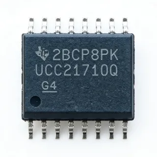
UCC21732-Q1 - ±10A Isolated SiC/IGBT Gate Driver | TI
部品番号: UCC21732-Q1 ✓ 生産中| 数量 | 単価 | 小計 |
|---|---|---|
| 1 | $5.9 | $5.90 |
| 10 | $5.31 | $53.10 |
| 100 | $4.72 | $472.00 |
| 500 | $4.25 | $2,125.00 |
| 1,000 | $3.78 | $3,780.00 |
| 3,000 | $3.35 | $10,050.00 |
UCC21732-Q1 概要
An isolated gate driver is a semiconductor device that translates a low-voltage PWM command from a controller into a high-current drive signal referenced to the floating gate of a high-voltage power switch (IGBT, SiC MOSFET, GaN HEMT), while providing galvanic isolation between the low-voltage domain and the high-voltage switching node. Within the broader taxonomy, isolated gate drivers sit below MOSFET/IGBT drivers and above optocouplers or transformer-based gate-drive solutions in the power management IC hierarchy.
Key features include 5.7 kV RMS reinforced isolation, >150 V/ns common-mode transient immunity (CMTI), integrated 2-level turn-off (STO) for short-circuit protection, and an analog sensing pin (AIN) for temperature or voltage monitoring. The driver supports both unipolar and bipolar gate-drive supplies and is qualified to AEC-Q100 for automotive applications.
The UCC21732-Q1 uses TI's SiO2 capacitive isolation technology, delivering 12.8 kV PK surge immunity, longer than 40 years of isolation barrier life, and low part-to-part propagation skew. On-board protection includes DESAT detection, soft turn-off, undervoltage lockout (UVLO) on both VCC and VDD, and an open-drain fault flag for the controller.
Typical applications include 800 V automotive traction inverters, EV on-board chargers (OBC), industrial servo drives, solar string inverters, and high-power DC fast-charging stations. The high CMTI and 900 mA soft-turn-off current make it well suited to high-switching-speed SiC FETs where dv/dt noise can otherwise corrupt the gate signal.
When designing with this driver, place the bootstrap or isolated supply decoupling capacitors as close to the VCC/VEE/VB/VS pins as possible and keep the DESAT and AIN traces short to avoid false triggering. Choose external gate resistors to balance switching loss and EMI.
This page synthesizes manufacturer datasheet parameters, distributor pricing, drop-in alternatives, and practical design notes not collated in the original TI datasheet PDF.
ドロップイン代替品: UCC21732-Q1 — 同一パッケージでピン互換。PCBの作り直しが必要な異なるパッケージの部品は除外されています。
このシリーズのバリエーション
同一シリーズでドロップイン互換のモデル: UCC21732-Q1 (同一形状・フットプリント) — 相違点: Package, Isolation Technology, Maximum DC Operating Voltage, Operating Temperature Range, Protection Features.
クイック比較ツール — 並列比較する代替部品を選択:
UCC21732
✅ ドロップイン📋 参考代替品(カタログ未掲載)
UCC21710-Q1
✅ ドロップイン✓ 在庫あり
価格はお問い合わせください
データシートを見る →UCC21750-Q1
✅ ドロップイン✓ 在庫あり
$3.45 / 個
データシートを見る →UCC21736-Q1
✅ ドロップイン📋 参考代替品(カタログ未掲載)
UCC21739-Q1
✅ ドロップイン📋 参考代替品(カタログ未掲載)
UCC21738-Q1
✅ ドロップイン📋 参考代替品(カタログ未掲載)
UCC21732-Q1 最大定格&電気的特性
| 機能 | Galvanic isolated single-channel gate driver |
| Target Switches | SiC MOSFET, IGBT |
| Maximum DC Operating Voltage | 2121 V |
| Peak Source Current | +10 A |
| Peak Sink Current | -10 A |
| Isolation Voltage (RMS) | 5.7 kV |
| Surge Immunity | 12.8 kV PK |
| Common-Mode Transient Immunity (CMTI) | >150 V/ns |
| Isolation Technology | SiO2 capacitive |
| Part-to-Part Skew | Low (per datasheet) |
| Soft Turn-Off (STO) Current | 900 mA |
| Number of Channels | 1 |
| パッケージ | 16-SOIC (DW) wide-body |
| 動作温度範囲 | -40 C to +125 C |
| Qualification | AEC-Q100 automotive |
| Protection Features | DESAT, 2-level turn-off, UVLO (VCC/VDD), fault flag |
| Analog Sense Input | AIN pin for temperature/voltage monitoring |
| RoHS ステータス | Compliant |
| Lead-Free | Yes |
UCC21732-Q1 ピン構成
| ピン 1 | VDD — Primary-side supply voltage (3.3 V or 5 V) |
| ピン 2 | GND1 — Primary-side ground |
| ピン 3 | IN+ — Non-inverting PWM input |
| ピン 4 | IN- — Inverting PWM input |
| ピン 5 | FLT — Open-drain fault output (active low) |
| ピン 6 | RDY — Power-good / ready output |
| ピン 7 | NC — Not connected (per datasheet) |
| ピン 8 | GND1 — Primary-side ground |
| ピン 9 | VCC — Secondary-side positive supply |
| ピン 10 | VEE — Secondary-side negative supply (tie to COM for unipolar) |
| ピン 11 | OUT — Gate-drive output to power switch |
| ピン 12 | VS — Source/emitter return for gate-drive loop |
| ピン 13 | DESAT — Desaturation detection input |
| ピン 14 | AIN — Analog sense input (temperature/voltage) |
| ピン 15 | NC — Not connected (per datasheet) |
| ピン 16 | COM — Secondary-side common reference |
主な用途
UCC21732-Q1 の用途: 7 件s: 800V EV Traction Inverter, EV On-Board Charger (OBC), Industrial Servo Drive, Solar String Inverter, DC Fast Charging Station, Wind Turbine Converter, Telecom DC-DC Converter.
800V EV Traction Inverter
Drives SiC MOSFET power modules in 800 V traction inverters with >150 V/ns CMTI. The UCC21732-Q1's 2121 V DC operating rating and 5.7 kV RMS reinforced isolation exceed the requirements of 800 V battery systems, while the ±10 A peak drive current ensures fast switching of high-charge SiC modules. Placed between the low-voltage VCU and the high-voltage DC-link switching node, it provides reinforced galvanic isolation mandated for automotive functional safety. The integrated 2-level turn-off (STO) at 900 mA safely discharges the SiC gate during a short-circuit event, limiting fault-current peak and protecting the expensive SiC module.
おすすめ
EV On-Board Charger (OBC)
Powers SiC or IGBT switches in 6.6 kW to 22 kW on-board charger PFC and DCDC stages. The UCC21732-Q1's wide 2121 V DC rating handles the rectified 800 V bus, while its capacitive SiO2 isolation simplifies the OBC's functional-isolation architecture. With ±10 A source/sink capability it drives mid-power SiC FETs at 100 kHz+ switching frequencies, reducing the size of magnetics and filter capacitors. The AIN pin can directly interface an NTC thermistor inside the power module for real-time temperature monitoring, enabling OBC thermal derating without an extra sensor ADC.
おすすめ
Industrial Servo Drive
Drives IGBT modules in industrial 400 V / 690 V servo drives with high reliability and reinforced isolation. The UCC21732-Q1's >150 V/ns CMTI rejects ground-noise transients generated by long motor cables, while the 16-SOIC (DW) wide-body package provides the 8 mm creepage required by IEC 61800-5-1 for industrial motor-drive reinforced isolation. The integrated DESAT detection and 2-level turn-off prevent shoot-through and short-circuit destruction of expensive IGBT modules, lowering warranty cost in factory automation.
おすすめ
Solar String Inverter
Drives 1500 V DC IGBT or SiC MOSFET modules in three-phase string inverters for utility-scale PV plants. The UCC21732-Q1's 2121 V DC operating voltage comfortably exceeds the 1500 V DC maximum string voltage, leaving margin for transient over-voltage events. Its 5.7 kV RMS reinforced isolation meets IEC 62109-1 requirements for PV converters without a separate opto-isolator. With 12.8 kV PK surge immunity, the driver tolerates nearby lightning-induced transients common on outdoor PV installations.
おすすめ
DC Fast Charging Station
Powers 350 kW+ DC fast-charging modules using 1000 V or 1200 V SiC half-bridges. The UCC21732-Q1's ±10 A peak drive enables fast switching of large SiC modules at 50-100 kHz, minimizing charger cabinet size. Its reinforced 5.7 kV RMS isolation is mandatory per IEC 61851-23 for EV charging. The 900 mA STO current is critical for protecting SiC MOSFETs from short-circuit failure when an EV battery is connected in a fault condition.
おすすめ
Wind Turbine Converter
Drives 1700 V IGBT stacks in the back-to-back AC-DC-AC converter of multi-MW wind turbines. The UCC21732-Q1's wide 2121 V DC operating range supports the high DC-link voltages used in modern wind converters, while its AEC-Q100 qualification (despite non-automotive application) provides the high reliability demanded by 25-year turbine service life. The AIN pin monitors IGBT-module baseplate temperature via NTC, enabling turbine derating before thermal limits are reached.
おすすめ
Telecom DC-DC Converter
Drives 100 V / 150 V-rated SiC MOSFETs in 48 V-to-400 V telecom rectifier stages. The UCC21732-Q1's capacitive isolation technology offers >40-year barrier life at continuous high-voltage operation, matching the long service life expected of telecom power shelves. With ±10 A peak drive and >150 V/ns CMTI, it enables high-frequency (>100 kHz) switching that reduces bulk capacitor and inductor size in the rectifier, increasing power density per rack unit.
おすすめ
おすすめ製品の概要
エンジニアリング参考データ: UCC21732-Q1 — 比較、設計ガイダンス、コンプライアンス情報。
選定ガイド
代替品との比較
| パラメータ | この製品 | UCC21732 | UCC21710-Q1 | UCC21750-Q1 | UCC21736-Q1 |
|---|---|---|---|---|---|
| Brand | Texas Instruments | Texas Instruments | Texas Instruments | Texas Instruments | Texas Instruments |
| Package | 16-SOIC (DW) wide-body | 16-SOIC (DW) wide-body - same | 16-SOIC (DW) wide-body - same | 16-SOIC (DW) wide-body - same | 16-SOIC (DW) wide-body - same |
| Automotive Grade (AEC-Q100) | Yes | No (industrial) | Yes | Yes | Yes |
| Isolation Voltage (RMS) | 5.7 kV | 5.7 kV | 5.7 kV | 5.7 kV | 5.7 kV |
主な差別化要因
- ±10 A peak drive with 900 mA STO for high-charge SiC (vs UCC21710-Q1)
- AEC-Q100 automotive qualified (vs UCC21732 (industrial))
- 12.8 kV PK surge immunity with >40-year barrier life (vs UCC21750-Q1)
設計ノート
Place the VCC-to-VEE and VB-to-VS decoupling capacitors as close as possible to the driver IC pins, with the loop area kept to a minimum to minimize parasitic inductance in the gate-drive loop. Use a 1 uF ceramic in parallel with a 0.1 uF ceramic for both supplies. Keep the gate-drive output traces short (under 25 mm) and use a ground plane on the secondary side to reduce dv/dt-induced ringing on the gate of the SiC/IGBT.
Estimated: the UCC21732-Q1 in 16-SOIC (DW) wide-body dissipates negligible power at idle but may dissipate 0.3-0.5 W at 100 kHz switching into a heavily capacitive SiC gate (typical gate charge 200-400 nC). At 25 C ambient this yields ~10-15 C temperature rise on the junction; no heatsink is required. Ensure the surrounding copper pour does not exceed thermal-stress limits on the SOIC body, especially under automotive thermal-cycling profiles.
For unipolar gate-drive supplies, the VEE pin must be tied directly to COM (secondary-side ground); do not leave it floating. DESAT blanking time must be tuned to avoid false triggering during normal turn-on transients - start at 200 ns and adjust per module. The AIN pin requires an external pull-up resistor or current source as shown in the TI evaluation board; floating it will produce undefined behavior. The FLT pin is open-drain and needs an external pull-up to VDD.
Maintain at least 8 mm creepage and clearance between primary-side (IN+, IN-, FLT, VDD, GND1) and secondary-side (OUT, VCC, VEE, VS, DESAT, AIN, COM) traces on the PCB, per IEC 60747-17 reinforced isolation requirements. Avoid running primary-side signal traces beneath the SOIC body or the isolation barrier - use a slot or keep-out region. The exposed pad (if any) must be soldered to a defined copper plane to provide thermal conduction and EMI shielding.
The UCC21732-Q1's >150 V/ns CMTI specification requires that input-side PWM traces be kept short and routed away from high-dv/dt switching nodes. Add a small RC filter (e.g., 100 ohm + 100 pF) on the IN+ and IN- pins only if PWM ringing exceeds the IC's input thresholds; do not over-filter and risk missing the SiC minimum on-time. Tie unused inputs to a defined logic level rather than floating.
コンプライアンス情報
AEC-Q100 qualified per the TI UCC21732-Q1 datasheet. RoHS and REACH compliant per TI product page. Lead-free and halogen-free per TI package materials declaration.