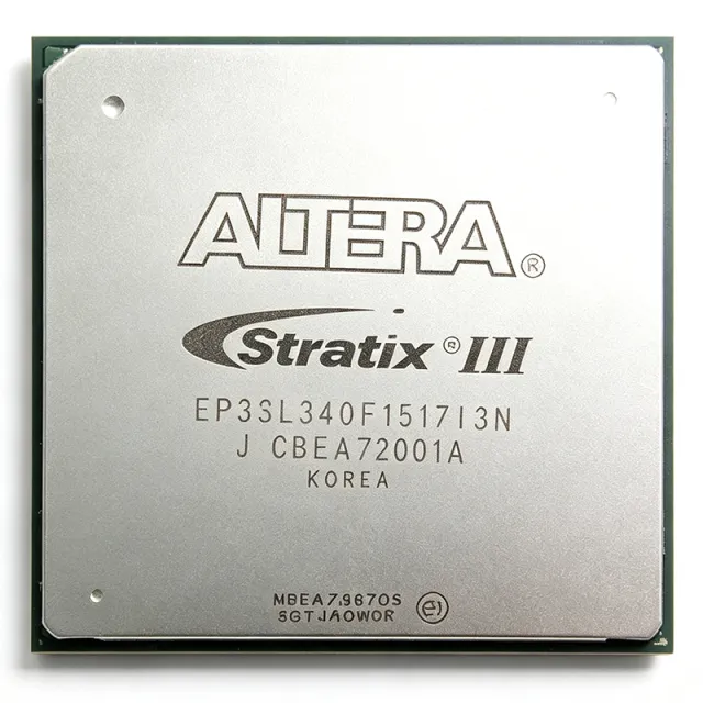
EP3SL340F1517C3
EP3SL340F1517C3 - 337,500-Cell FPGA | Intel | Digital Logic
Intel EP3SL340F1517C3 is a high-density Stratix III L FPGA built for programmable digital systems requiring substantial logic capacity and extensive external interfacing. Its verified headline parameters are 337,500 logic cells, 976 user I/O pins, and 13,500 LABs, housed in a 1517-ball FCBGA package. This combination places the device in the FPGA and CPLD category while supporting designs that need many parallel interfaces, custom datapaths, and reconfigurable processing logic.
An FPGA, or field-programmable gate array, is a semiconductor device containing programmable logic blocks, routing resources, memory elements, and configurable I/O. Engineers configure these resources to implement digital functions after manufacturing. In the system hierarchy, EP3SL340F1517C3 belongs to FPGA devices, programmable logic, digital integrated circuits, and ultimately semiconductors. Unlike a fixed-function ASIC, the FPGA can be revised through configuration data without changing the silicon device.
The verified 337,500-cell capacity supports large control engines, interface aggregation, and custom high-speed digital functions. The device provides 976 I/O pins for connecting numerous peripheral buses, memory interfaces, converters, and control signals. Its 13,500 LABs provide a broad fabric for implementing combinational and sequential logic. The 1517-pin FCBGA package offers high interconnection density but requires advanced PCB design, controlled impedance routing, reliable power distribution, and careful thermal management.
The part is identified as a 65 nm Stratix III L device with a 500 MHz specification reported by the supplied FPGAkey result and a 1.1 V core-voltage value also reported there. Another distributor result describes 18,822,144 bits and 337,500 logic elements/cells. These values establish a large programmable architecture, but detailed timing, transceiver count, memory capacity, operating temperature, and package dimensions remain subject to the manufacturer datasheet. The configuration interface, supported I/O standards, embedded resources, and exact speed grade must be confirmed before release to production.
Typical applications include communications equipment, industrial automation, test and measurement, video and imaging systems, and high-channel-count data acquisition. In these systems, the FPGA can consolidate control logic, protocol conversion, parallel data processing, and timing functions into one programmable platform. The 976 I/O count is particularly useful where many external devices or parallel buses must be connected.
Designers should treat the FCBGA as a high-density system-in-package challenge rather than a conventional low-pin-count IC. Validate the complete Intel pin assignment, power-up sequence, decoupling network, signal-integrity constraints, and thermal solution from the manufacturer documentation. A board redesign is normally required when moving to another FPGA family, density, package, or pinout.
This data set combines verified distributor specifications, package information, indicative commercial data, and clearly marked engineering gaps. It is intended to support early component selection, sourcing research, and architecture planning, not to replace the manufacturer datasheet, qualification records, or final signal-integrity and thermal analysis.
견적 요청
문의하기