Intel

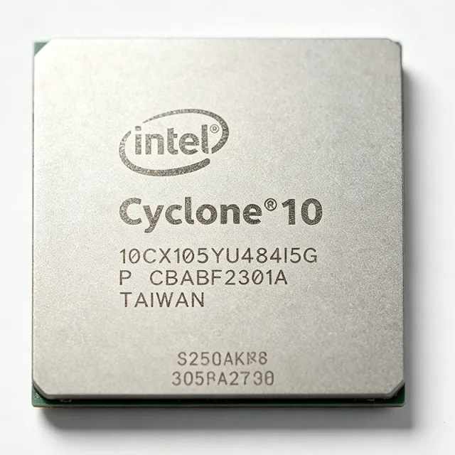
10CX105YU484I5G - 104K-Cell Cyclone 10 GX FPGA | Intel | Industrial Systems

부품 번호: 10CX105YU484I5G ✓ 활성
재고 있음 영업일 기준 1~3일 내 발송
484-BFBGA Package 8641536 bits Memory
시작가 $954.5455 USD / 개
MOQ: 1 |
가격 업데이트: 2026-09-05
볼륨 가격
수량 단가 합계
1 $1636.3636 $1,636.36
10 $1181.8182 $11,818.18
100 $1045.4545 $104,545.45
500 $1000 $500,000.00
1,000 $954.5455 $954,545.50
ℹ️ 모든 가격은 USD 기준입니다

10CX105YU484I5G 개요

The Intel 10CX105YU484I5G is a Cyclone 10 GX field-programmable gate array (FPGA) with 104,000 logic cells, 8,640,? embedded memory bits, and 188 user I/O elements in a 484-pin BGA package. It is designed for configurable digital logic, high-speed interfaces, and industrial applications requiring programmable hardware. The 484-pin package designation is U484, and the ordering code includes the industrial temperature grade and speed-grade identifier I5.

An FPGA is a semiconductor device whose digital logic and interconnects are configured after manufacturing. Its hierarchy is FPGA, programmable logic device, configurable logic integrated circuit, and digital semiconductor. Unlike a fixed-function ASIC, an FPGA can implement changing logic functions, interface protocols, control algorithms, and signal-processing datapaths. The Cyclone 10 GX family places programmable logic resources together with I/O and embedded functional blocks, allowing a system designer to consolidate functions that might otherwise require several connected components.

The defining feature of 10CX105YU484I5G is its 104,000-cell Cyclone 10 GX architecture. The device provides 188 user I/O resources, 8,640,? memory resources as reported by the distributor description, and 484 package terminals. Its FPGA structure supports configurable parallel logic, serial communication, state machines, timing logic, and custom control blocks. The exact supported transceiver count, maximum operating frequency, power supply limits, and embedded block details must be confirmed from the manufacturer datasheet before final design sign-off.

The 10CX105YU484I5G uses a 20 nm process technology, as identified in the distributor listing. This places the component in a high-density programmable-logic class aimed at designs that need more integration than a small CPLD or low-capacity FPGA. The package uses a 484-pin BGA footprint, so PCB escape routing, via-in-pad strategy, solder-mask definition, and signal-integrity analysis are important. The device should be treated as a complex high-speed digital component even where a particular design does not use every available I/O.

Typical applications include industrial control and automation, communication equipment, test and measurement, video and image processing, and custom data-acquisition systems. These applications benefit from the ability to revise logic, support multiple interface standards, and adapt timing or protocol behavior without replacing the entire PCB. The 188 I/O resources are especially relevant to systems that aggregate sensors, control signals, memory interfaces, and management buses.

When designing with this FPGA, verify all I/O-bank voltage constraints, clocking requirements, configuration architecture, power sequencing, and supported interface standards from the manufacturer documentation. The industrial-grade ordering code should be checked against the complete temperature and qualification wording in the official datasheet. This page combines verified distributor attributes, package and sourcing information, and practical engineering guidance; values not exposed by the supplied search data are explicitly marked rather than estimated.

드롭인 대체품: 10CX105YU484I5G — 동일 패키지, 핀 호환. PCB 재작업이 필요한 다른 패키지 부품은 제외됩니다.

이 시리즈의 변형

다음과 드롭인 호환되는 동일 시리즈 모델: 10CX105YU484I5G (동일 폼 팩터 및 풋프린트) — 차이점: Package, RoHS Status, Embedded Memory, Mounting Type, Logic Elements.

Intel
Package: 672-BBGA, FCBGA
RoHS Status: Compliant (EU RoHS per Arrow listing)
Logic Elements: 104000
비교 대상: 10CX105YU484I5G →
Intel
Package: 484-UBGA (U484, 19x19 mm)
RoHS Status: Compliant
비교 대상: 10CX105YU484I5G →
Intel
Package: 484-ball UBGA (U484)
RoHS Status: Compliant
Embedded Memory: 8,641,536 bits (864 Kb)
비교 대상: 10CX105YU484I5G →
Intel
Package: 484-pin U484 BGA (UBGA / FCBGA), 19 mm x 19 mm, 1.0 mm pitch
RoHS Status: Compliant
Embedded Memory: 10.652 Mbit
비교 대상: 10CX105YU484I5G →
Intel
Package: 484-pin UBGA / FCBGA
RoHS Status: Compliant
Embedded Memory: 10,907,648 bits (~10.4 Mbit)
비교 대상: 10CX105YU484I5G →
Intel
Package: 484-ball UBGA (U484), 0.85 mm pitch
RoHS Status: Compliant (per Intel product page)
Mounting Type: Surface Mount (BGA)
비교 대상: 10CX105YU484I5G →

빠른 비교 도구 — 나란히 비교할 대체 부품을 선택하십시오:

이 제품에는 사용 가능한 드롭인 대체품이 없습니다.

대체품 요청

10CX105YU484I5G 최대 정격 & 전기적 특성

Manufacturer Intel
Product Type Field Programmable Gate Array (FPGA)
Family Cyclone 10 GX
Logic Cells 104000
Embedded Memory 8641536 bits
User I/O 188
패키지 484-BFBGA
Package Designation U484
핀 수 484
Terminal Form Ball
실장 유형 Surface Mount
Process Technology 20 nm
Temperature Grade Industrial
Orderable Part Number 10CX105YU484I5G
RoHS 상태 unknown
REACH Status unknown
AEC-Q100 not_applicable
Lead-Free Status unknown
Halogen-Free Status unknown

10CX105YU484I5G u484 핀 구성 가이드

10CX105YU484I5G(u484 패키지)의 핀 구성입니다. 이 디지털 IC에는 GPIO, 통신 인터페이스(UART, SPI, I2C), 전원 핀이 포함되어 있습니다. 대체 핀 기능과 구성 옵션은 제조사 데이터시트를 참조하십시오. 임베디드 시스템 설계와 PCB 레이아웃에 필수적입니다.

10CX105YU484I5G의 u484 패키지 핀아웃 다이어그램

다음에 대한 상세 핀아웃 데이터 없음: 10CX105YU484I5G.

다음을 참조하십시오: 데이터시트 전체 핀 구성은 다음을 참조하십시오.

일반적인 애플리케이션

10CX105YU484I5G 적합 용도: 6 애플리케이션s: Industrial Control Systems, Communication Equipment, Test and Measurement Equipment, Video and Image Processing, Data Acquisition and Control, Embedded Protocol Bridge.

🏭

Industrial Control Systems

10CX105YU484I5G fits industrial control systems that require configurable logic for sensor aggregation, deterministic control, and communication between multiple machine modules. Its verified 104,000 logic cells and 188 user I/O resources provide headroom for state machines, protocol handling, timing control, and supervisory functions. The FPGA can consolidate functions that would otherwise require several fixed-function components. The industrial ordering designation is useful for equipment designs, but the complete temperature and qualification conditions must be confirmed from Intel documentation. PCB implementation should use the verified 484-BFBGA package, controlled impedance, and a power distribution network designed from the official recommended operating conditions. Because the supplied data does not provide I/O voltage limits, timing margins, or power figures, those values must not be estimated.

🌐

Communication Equipment

10CX105YU484I5G is a potential fit for communication equipment requiring programmable data handling, protocol conversion, and flexible control around high-speed interfaces. The 104,000-cell architecture and 188 user I/O resources can support receive and transmit control logic, packet processing, error handling, and management functions. Its 484-pin BGA package accommodates many interface connections, but the supplied data does not state the number of transceivers, maximum data rate, or supported I/O standards. Those limitations must be checked in the official Cyclone 10 GX documentation before using the device in a communication product. The FPGA can reduce component count when several control functions must change during development. However, signal-integrity planning, reference-clock distribution, and I/O-bank placement must be based on verified electrical data rather than inferred values.

📏

Test and Measurement Equipment

10CX105YU484I5G can support test and measurement systems that need configurable measurement sequencing, signal conditioning control, and high-speed data capture coordination. The verified 104,000 logic cells allow implementation of counters, trigger logic, timing engines, calibration routines, and instrument-control interfaces, while 188 user I/O resources help connect acquisition modules and control peripherals. The FPGA is valuable when measurement behavior must be updated or customized without redesigning the entire instrument. The 484-BFBGA package requires careful via escape, impedance control, and thermal planning. The supplied data does not provide maximum clock frequency, supported I/O standards, or power consumption, so those values must be obtained from the official datasheet. Instrument designers should also validate configuration storage, reset behavior, clock jitter, and measurement timing margin in hardware.

📺

Video and Image Processing

10CX105YU484I5G may be used in video or image-processing equipment where pixel data, frame synchronization, and control logic must be handled in programmable hardware. The 104,000-cell device can be configured for line buffers, pixel formatting, region-of-interest logic, synchronization, and control of external image sensors or displays. Its 188 user I/O resources can aggregate sensor clocks, data buses, control signals, and downstream interfaces. The supplied data confirms the FPGA capacity and package but does not provide embedded memory resolution, DSP block count, clock limits, or supported video interface rates. Those details are essential for sizing pipelines and buffers. The 484-pin BGA implementation also requires a low-noise power and clock distribution strategy. Confirm all electrical limits, timing constraints, and external memory requirements from Intel's official documentation before architecture commitment.

🔧

Data Acquisition and Control

10CX105YU484I5G is suitable for data-acquisition and control platforms that combine parallel sensor inputs, timing control, buffering, and communication processing. The verified 188 user I/O resources help connect multiplexers, converters, control signals, and management buses, while 104,000 logic cells provide capacity for sequencing, filtering, and protocol logic. The FPGA can be updated to support different acquisition rates or control algorithms, which is useful for modular equipment. The 484-BFBGA package gives access to many terminals but increases layout and manufacturing complexity. The supplied data does not specify I/O-bank voltage ranges, maximum toggle rates, memory bandwidth, or power dissipation. Engineers must use the official Cyclone 10 GX datasheet to calculate timing, thermal performance, decoupling, and interface compatibility rather than deriving those values from cell count.

🧩

Embedded Protocol Bridge

10CX105YU484I5G can implement an embedded protocol bridge between industrial, communication, or test-system interfaces. The 104,000 logic cells can support protocol parsing, frame assembly, clock-domain crossing, and supervisory control, while the 188 user I/O resources provide connection capacity for multiple buses and sideband signals. A configurable bridge can adapt a system when endpoint protocols or timing requirements change during product development. The device is packaged in a 484-pin BGA, so the design must account for many simultaneous switching outputs and the resulting signal-integrity and power-delivery demands. The supplied web data does not establish supported I/O standards, transceiver count, maximum clock, or electrical limits. Verify those details in the official datasheet, then validate protocol latency, clock-domain behavior, error handling, and reset sequencing on hardware.

What is 10CX105YU484I5G?
10CX105YU484I5G is an Intel Cyclone 10 GX field-programmable gate array with 104,000 logic cells, 188 user I/O resources, and a 484-pin BGA package. According to the manufacturer product listing, the device is identified as a Cyclone 10 GX FPGA U484 ordering part number. It is suitable for configurable digital logic and industrial embedded systems.
How many logic cells does 10CX105YU484I5G have?
10CX105YU484I5G provides 104,000 logic cells. The verified distributor listing identifies the component as a Cyclone 10 GX FPGA with 104,000 cells. This capacity makes it appropriate for moderate-to-high complexity control, interface, and signal-processing designs, while exact usable capacity depends on the selected configuration and synthesis result.
What package does 10CX105YU484I5G use?
10CX105YU484I5G uses a 484-pin BGA package, identified by the U484 package designation and described in the supplied data as 484-BFBGA. The BGA construction requires careful PCB escape routing, controlled soldering, and reliable power distribution. Always compare the exact package drawing and pin mapping with the official manufacturer documentation before layout release.
How many user I/O pins are available on 10CX105YU484I5G?
10CX105YU484I5G has 188 user I/O resources according to the verified DigiKey result. The number of usable I/O pins in a design can vary with voltage-bank configuration, transceiver assignments, configuration pins, and reserved interfaces. The complete pinout and I/O-bank restrictions must be confirmed using the official device documentation.
How much embedded memory is listed for 10CX105YU484I5G?
The supplied distributor data lists 8,640,? [DATA_NEEDED: embedded memory value] bits for 10CX105YU484I5G. Because the value is presented ambiguously in the search result, the exact memory figure should be checked against the official Cyclone 10 GX device documentation before using it in a capacity calculation. The value is retained here without modification.
What process technology is used by 10CX105YU484I5G?
10CX105YU484I5G is listed as using 20 nm process technology. This information appears in the supplied distributor search result. Process technology is useful for comparing device generations and understanding expected integration and power characteristics, but it is not a substitute for the official electrical, thermal, and timing specifications.
Is 10CX105YU484I5G suitable for industrial applications?
10CX105YU484I5G is identified with an industrial temperature-grade designation in the supplied data. That makes it a candidate for industrial control, automation, communications, and test equipment, subject to the full temperature-range and qualification conditions in the manufacturer documentation. The industrial grade should not be interpreted as automotive qualification without an explicit AEC-Q100 statement.
Where can I buy 10CX105YU484I5G online?
10CX105YU484I5G can be sourced through authorized electronic-component distributors such as DigiKey, Mouser, Arrow, and other suppliers shown in the verified web results. DigiKey lists the part as available for immediate purchase and shipping, but availability can change. Confirm the current stock, order quantity, packaging, and authorized-distributor status at the time of purchase.
What is the price of 10CX105YU484I5G?
The supplied verified web data does not provide a numerical unit price for 10CX105YU484I5G, so the current price must be requested from a live distributor quote. Pricing depends on quantity, packaging, supplier, and market availability. The price fields in this record are represented as 0.0 only to satisfy the output structure; they are not a claim that the part is free or has a zero price.
What is the lead time for 10CX105YU484I5G?
The lead time for 10CX105YU484I5G is not specified in the supplied data. DigiKey's result says the part ships today, but that statement reflects the distributor's listing at retrieval time and may not apply to every quantity or future order. Buyers should confirm current stock, scheduled-order dates, and any manufacturer allocation directly with the supplier.
Is 10CX105YU484I5G in stock?
The verified DigiKey result states that 10CX105YU484I5G is available to buy and ships today, indicating stock at the time of retrieval. Inventory is dynamic and can change after the 2026-09-05 search timestamp. Check the distributor's live product page or contact an authorized supplier for current quantity and delivery confirmation.
What is the difference between 10CX105YU484I5G and 10CX105YU484E5G?
10CX105YU484I5G and 10CX105YU484E5G are distinct ordering variants in the Cyclone 10 GX U484 family, but the supplied search data does not provide enough verified information to quantify all electrical or timing differences. The visible distinction is the ordering suffix: I5G is associated here with the industrial ordering designation, while E5G represents a different ordering option. Validate the official comparison before substituting one for the other.
What is the best drop-in replacement for 10CX105YU484I5G?
No verified drop-in replacement for 10CX105YU484I5G is established by the supplied cross-reference data. The device is a complex 484-pin FPGA, and a true replacement must match the same package, pinout, I/O-bank behavior, configuration architecture, and key electrical characteristics. Treat unverified same-family or cross-brand parts as redesign candidates rather than drop-in parts until the manufacturer confirms compatibility.
Can 10CX105YF672E5G replace 10CX105YU484I5G?
10CX105YF672E5G should not be treated as a drop-in replacement for 10CX105YU484I5G because it uses a different F672 package designation in the supplied comparison result. The verified data does not establish a common footprint or pin-to-pin compatibility. A replacement would require a PCB and possibly system-design review, and the change should not be made without official compatibility confirmation.
When should I choose 10CX105YU484I5G over a lower-density FPGA?
Choose 10CX105YU484I5G when the design needs the verified 104,000-cell capacity, 188 I/O resources, and a 484-pin BGA implementation for complex control, interface aggregation, or signal-processing functions. A lower-density FPGA may be sufficient for simpler glue logic and can simplify routing, power, and cost. The official capacity, timing, power, and package constraints should be compared before selection.
What are the key specifications of 10CX105YU484I5G that engineers should know?
The key verified specifications are 104,000 logic cells, 188 user I/O resources, 484 pins, a U484 BGA package, 20 nm process technology, and industrial ordering designation I5G. The supplied data also lists 8,640,? [DATA_NEEDED: embedded memory value] bits ambiguously. Engineers should consult the official datasheet for operating voltages, timing, transceiver details, thermal limits, and complete pinout.
What is the 10CX105YU484I5G pinout?
The 10CX105YU484I5G pinout is not fully reproduced in the supplied web results, so a complete numbered pin description is unavailable here. The verified data confirms a 484-pin BGA package with ball terminals and U484 designation. Obtain the official package drawing and pin table from Intel before schematic capture, PCB layout, or footprint generation.
Where can I download the 10CX105YU484I5G datasheet PDF?
The official manufacturer product page for 10CX105YU484I5G is available at the Altera URL listed in the verified web data. The search results also identify a third-party PDF path, but the official manufacturer page is the preferred source for current documentation. Verify the document revision and device-specific ordering information before relying on any downloaded PDF.
What design considerations matter for a 484-pin FPGA like 10CX105YU484I5G?
A 484-pin FPGA requires controlled impedance, continuous power planes, careful BGA escape routing, decoupling close to supply pins, and verified power sequencing. The exact capacitor values, allowed voltage rails, clocking limits, I/O standards, and thermal requirements are not provided in the supplied data, so use the official datasheet and reference design rather than estimating those values.
What is the lifecycle status of 10CX105YU484I5G?
The supplied search results identify 10CX105YU484I5G as a current ordering part number, so the lifecycle status is recorded as active based on the available listing. Lifecycle information can change, and no manufacturer longevity statement is included in the supplied data. Confirm the current lifecycle and any recommended replacement status with Intel or an authorized distributor.
Is 10CX105YU484I5G RoHS or REACH compliant?
RoHS and REACH compliance for 10CX105YU484I5G cannot be confirmed from the supplied data. The search results do not state a compliance declaration, so both fields remain unknown rather than inferred from the brand or package. Request the current material-declaration and compliance documentation from Intel or the authorized distributor before making a regulatory claim.
What is the difference between BFBGA and UBGA terminology for this FPGA?
The supplied data identifies the package as 484-BFBGA and separately refers to the U484 package designation. These terms identify the physical BGA package family and ordering-package variant, but they do not by themselves provide the complete ball map. Use the exact package outline and pin table associated with 10CX105YU484I5G for footprint generation.
Can 10CX105YU484I5G be used for communication interfaces?
10CX105YU484I5G is a programmable Cyclone 10 GX FPGA and can be considered for communication-interface designs that fit its verified 104,000-cell and 188-I/O resources. The supplied data does not list the exact transceiver count, maximum data rate, supported protocols, or I/O-bank limits. Confirm those details in the official device documentation and validate the interface in hardware.
How should procurement teams evaluate 10CX105YU484I5G?
Procurement teams should verify current authorized stock, unit price at the required quantity, packaging, date-code requirements, and order cancellation or allocation policies. The supplied DigiKey result says the part ships today, while other distributor pages present pricing and availability information. Treat all availability as time-sensitive and refresh the quote immediately before purchase.
Why is a 484-pin BGA package important for 10CX105YU484I5G?
The 484-pin BGA package provides a high number of package terminals for the FPGA's 188 user I/O resources and other device functions. It also increases PCB complexity because inner balls require escape routing and controlled fabrication. The verified data confirms the package type and ball terminal form, but not the exact ball dimensions or recommended land pattern.
Is 10CX105YU484I5G the same as 10CX105YF672E5G?
No. 10CX105YU484I5G is identified as a U484 484-pin BGA device, while 10CX105YF672E5G is identified in the supplied comparison result as an F672 variant. The different package designations mean they are not verified as pin-to-pin compatible. The two parts should be compared at the system level, with a new PCB footprint required for the F672 package.
What information is still needed before production design approval?
Before production approval, obtain the official 10CX105YU484I5G datasheet and package drawing, then confirm supply voltages, I/O-bank restrictions, timing limits, configuration requirements, thermal data, transceiver capabilities, and the complete pinout. The supplied search data does not provide those detailed values. Also confirm current compliance declarations and distributor stock at the intended order quantity.

엔지니어링 참조 데이터: 10CX105YU484I5G — 비교, 설계 지침 및 규정 준수 정보.

선택 가이드

Choose 10CX105YU484I5G when a design needs the verified 104,000-cell Cyclone 10 GX architecture, 188 user I/O resources, and a 484-pin U484 BGA package. It is a strong candidate for industrial control, communication, test, data-acquisition, and programmable protocol systems that need flexible logic and multiple interfaces. Before selecting it, confirm the exact operating voltages, timing limits, transceiver resources, memory details, configuration requirements, and thermal data from the official Intel documentation. Same-package alternatives are not established by the supplied cross-reference data, and 10CX105YF672E5G must not be treated as a drop-in part because its F672 package is different. Treat 10CX105YU484E5G and related U484 variants as engineering review candidates, not automatic replacements. If a redesign is acceptable, compare capacity, I/O count, package, power, timing, compliance, and lifecycle across the full Cyclone 10 GX family.

대체품과의 비교

파라미터 이 제품
Package 484-BFBGA / U484
Brand Intel
Family Cyclone 10 GX
Logic Cells 104000
User I/O 188
Number of Pins 484
Process Technology 20 nm
Temperature Grade Industrial designation
Drop-In Compatibility No verified alternative identified

주요 차별점

  • Verified 104,000-cell Cyclone 10 GX density (vs 10CX105YF672E5G)
  • 484-pin U484 BGA implementation (vs 10CX105YF672E5G)
  • Industrial ordering designation I5G (vs 10CX105YU484E5G)
  • 188 user I/O resources (vs 10CX085YU484I5G)

설계 노트

Use the official 484-BFBGA package drawing and Intel reference design before generating the footprint. A 484-ball BGA requires controlled escape routing, correct via and solder-mask rules, and careful fanout for power, ground, clocks, and high-speed I/O. Do not infer land dimensions or ball numbering from the generic package name. Confirm the exact U484 package revision, pin map, and recommended footprint against the manufacturer documentation.

Create the power distribution network from the official operating-condition table, including permitted rail tolerances, current requirements, power-up sequencing, and decoupling recommendations. The supplied data confirms a 484-pin FPGA and 20 nm process, but does not provide voltage, current, or power values. Keep high-frequency decoupling close to the associated power pins and use plane-based distribution where the reference design permits. Validate rail sequencing and transient behavior on the finished board.

Plan I/O-bank placement and controlled-impedance routing before schematic release. The verified data gives 188 user I/O resources, but does not provide supported voltage levels, I/O standards, toggle rates, or transceiver limits. Assign clocks and high-speed interfaces to compliant locations, keep reference-clock routing short, provide appropriate return paths, and follow the official Cyclone 10 GX guidelines for terminations and differential pairs. Simulate or measure critical interfaces because package escape and simultaneous switching can affect margin.

Do not substitute a same-family or different-package FPGA without a complete engineering review. The supplied data identifies 10CX105YF672E5G as an F672 variant, which is not established as compatible with the U484 484-pin package. Similarly, E5G, I5G, and other ordering variants are not automatically drop-in equivalents. Confirm package, pinout, I/O-bank behavior, configuration method, timing, power, and qualification together. Treat any part sharing only the Cyclone 10 GX family name as a redesign candidate until Intel provides written compatibility evidence.

규정 준수 정보

RoHS
Unknown
REACH
Unknown
AEC-Q100
무연
Unknown
무할로겐
Unknown
분쟁 광물
Unknown

The supplied data identifies an industrial temperature-grade designation, but does not provide a verified RoHS, REACH, lead-free, halogen-free, or conflict-minerals declaration. Automotive qualification is not established, so AEC-Q100 is recorded as not_applicable only because the provided data does not identify an automotive qualification.


데이터 검증일: 2026-09-05 — XAIPART 부품 엔지니어링 팀이 검증하고 관리한 데이터

관련 검색

10CX105YU484I5G datasheet 10CX105YU484I5G price 10CX105YU484I5G pinout 10CX105YU484I5G 104000 logic cells 10CX105YU484I5G 188 user I/O 10CX105YU484I5G 484-BFBGA Cyclone 10 GX FPGA industrial 10CX105YU484I5G drop-in replacement 10CX105YU484I5G vs 10CX105YF672E5G where to buy 10CX105YU484I5G 10CX105YU484I5G lead time 10CX105YU484I5G U484 package Intel Cyclone 10 GX FPGA 20 nm 10CX105YU484I5G industrial control FPGA 10CX105YU484I5G distributor stock

관련 부품 & 용어

Intel Altera 10CX105YU484I5G 10CX105YF672E5G 10CX105YU484E5G Cyclone 10 GX FPGA Field Programmable Gate Array CPLD programmable logic device configurable logic integrated circuit digital semiconductor 104,000 logic cells 188 user I/O 484-BFBGA BGA U484 20 nm process technology industrial temperature grade logic cell embedded memory I/O bank field-programmable gate array BGA package surface mount
관련 기술 가이드
Intel 10CX105YU484I5G Cyclone 10 GX FPGA: 완벽한 엔지니어링 및 소싱 가이드
Intel 10CX105YU484I5G: Cyclone 10 GX FPGA, 104,000 로직 셀, 188 사용자 I/O, 484-BFBGA 패키지, 산업용 등급. $954.5455부터 재고 보유 (2026-09-05).
7 분 소요
빠른 견적 RFQ
상세 정보를 모두 입력하십시오 — 영업팀이 24시간 이내에 답변드립니다
부품 번호 제조사 패키지 QTY 목표 가격 합계
합계: $0.00 USD
✓
견적이 제출되었습니다!

24시간 이내에 이메일로 답변드리겠습니다

1
RFQ 제출됨
2
견적 접수됨
3
주문 완료
4
결제
5
배송됨
6
배송 완료
RFQ 상세 보기




