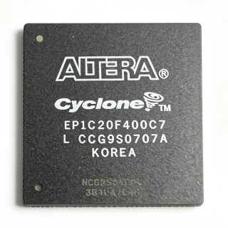
EP1C20F400I-6 - Cyclone FPGA 20,060 LE BGA-400 | Intel / Altera
부품 번호: EP1C20F400I-6 ✗ 단종| 수량 | 단가 | 합계 |
|---|---|---|
| 1 | $42.5 | $42.50 |
| 10 | $38.75 | $387.50 |
| 100 | $34.2 | $3,420.00 |
| 500 | $30.1 | $15,050.00 |
| 1,000 | $27.85 | $27,850.00 |
EP1C20F400I-6 개요
A Field-Programmable Gate Array (FPGA) is a semiconductor integrated circuit whose digital logic function is defined by user-loaded configuration memory rather than fixed mask layers, sitting in the broader hierarchy: programmable logic -> logic IC -> integrated circuit -> semiconductor. Cyclone was Altera's first family to explicitly target ASIC replacement in consumer, communications, and industrial DSP, and the EP1C20 sits at the upper end of that first-generation family.
Key features of the EP1C20F400I-6 include 20,060 logic elements, 294,912 bits of embedded RAM (M4K blocks), 244 embedded 18x18 multipliers (hard DSP blocks), up to 301 user I/O pins, four phase-locked loops for clock management, and support for LVDS, LVTTL, LVCMOS, SSTL, and PCI I/O standards. The -6 speed grade specifies the slowest of the Cyclone tiers, favoring power and yield over raw Fmax.
Architecturally, the EP1C20 uses a four-input look-up table (LUT) fabric with embedded multiplier blocks, dedicated M4K RAM blocks (4 Kbits each, true dual-port capable), and global clock networks routed through the four PLLs. Configuration is loaded from passive serial (PS), active serial (AS), or JTAG, with bitstream encryption available on higher tiers but not on Cyclone. The 400-ball FineLine BGA (1.0 mm pitch) provides ample routing escape for high I/O counts while keeping board complexity manageable.
Typical applications include digital signal processing for industrial control, glue logic and bus bridging in telecom line cards, video processing front-ends, low-cost automotive infotainment subsystems, and ASIC prototyping. The embedded 18x18 multipliers are particularly suited to FIR filters and FFT butterfly stages. Industrial-grade temperature range makes the device acceptable for factory automation and outdoor communications gear.
When designing with the EP1C20F400I-6, careful attention to power sequencing and decoupling is critical: the 1.5V VCCINT must ramp monotonically before VCCIO to avoid I/O latch-up. Use the Quartus II design software (or its modern equivalent) for synthesis, placement, and timing closure. Note that the Cyclone family is end-of-life; new designs should evaluate Cyclone IV/V or MAX 10 for active production.
This page synthesizes distributor stock data, parametric alternatives, and practical design notes that go beyond the original Altera Cyclone family datasheet, helping engineers determine whether to sustain an existing EP1C20 design or migrate to a modern equivalent.
드롭인 대체품: EP1C20F400I-6 — 동일 패키지, 핀 호환. PCB 재작업이 필요한 다른 패키지 부품은 제외됩니다.
이 시리즈의 변형
다음과 드롭인 호환되는 동일 시리즈 모델: EP1C20F400I-6 (동일 폼 팩터 및 풋프린트) — 차이점: Process Technology, Speed Grade, Package, Family, RoHS Status.
빠른 비교 도구 — 나란히 비교할 대체 부품을 선택하십시오:
EP1C20F400C8N
✅ 드롭인✓ 재고 있음
$62.5 / 개
데이터시트 보기 →EP1C20F400C7N
✅ 드롭인✓ 재고 있음
$65.8 / 개
데이터시트 보기 →EP1C20F400C6
✅ 드롭인✓ 재고 있음
$18.95 / 개
데이터시트 보기 →EP1C20F400
✅ 드롭인✓ 재고 있음
$58.9 / 개
데이터시트 보기 →EP1C20F400C8NAC
✅ 드롭인✓ 재고 있음
가격 문의
데이터시트 보기 →EP1C20F400C6N
✅ 드롭인✓ 재고 있음
$53.1 / 개
데이터시트 보기 →EP1C20F400I-6 최대 정격 & 전기적 특성
| Family | Cyclone (first generation) |
| Logic Elements | 20,060 |
| Embedded Memory (M4K blocks) | 294,912 bits (72 M4K blocks) |
| Embedded 18x18 Multipliers | 244 |
| Maximum User I/O Pins | 301 |
| Phase-Locked Loops (PLLs) | 4 |
| Speed Grade | -6 (slowest of Cyclone family) |
| Temperature Grade | Industrial (-40C to +85C) |
| 패키지 | 400-ball FineLine BGA (FBGA-400) |
| Pitch | 1.0 mm |
| Core Voltage (VCCINT) | 1.5 V |
| I/O Voltage (VCCIO) | Multiple banks, 1.5V to 3.3V |
| Process Technology | 0.13 um SRAM |
| Configuration Modes | Passive Serial (PS), Active Serial (AS), JTAG |
| Supported I/O Standards | LVTTL, LVCMOS, SSTL, LVDS, PCI |
| RoHS 상태 | Compliant (per distributor listings) |
| 수명 주기 상태 | End-of-Life (Cyclone family discontinued) |
EP1C20F400I-6 400-ball fineline bga (fbga-400) 핀 구성 가이드
EP1C20F400I-6(400-ball fineline bga (fbga-400) 패키지)의 핀 구성입니다. 이 디지털 IC에는 GPIO, 통신 인터페이스(UART, SPI, I2C), 전원 핀이 포함되어 있습니다. 대체 핀 기능과 구성 옵션은 제조사 데이터시트를 참조하십시오. 임베디드 시스템 설계와 PCB 레이아웃에 필수적입니다.

다음에 대한 상세 핀아웃 데이터 없음: EP1C20F400I-6.
다음을 참조하십시오: 데이터시트 전체 핀 구성은 다음을 참조하십시오.
일반적인 애플리케이션
EP1C20F400I-6 적합 용도: 6 애플리케이션s: Industrial Motor Control DSP, Telecom Line-Card Glue Logic and Bus Bridging, Video Processing Front-End, ASIC Prototyping and Emulation, Low-Cost Automotive Infotainment Subsystem, Test and Measurement Instrumentation.
Industrial Motor Control DSP
The EP1C20F400I-6's 244 embedded 18x18 multipliers deliver up to ~250 MHz multiply-accumulate throughput, enabling real-time FIR filtering and Park/Clarke transforms for closed-loop field-oriented control of AC induction and PMSM motors. The industrial -40C to +85C temperature grade ensures reliable operation in factory cabinets and outdoor variable-frequency drives without thermal derating, while the 301 user I/O pins accept multiple quadrature encoder, Hall-sensor, and resolver inputs simultaneously. Compared with a DSP+microcontroller architecture, integrating the control loop in a single Cyclone reduces BOM and PCB area, and the four PLLs provide deterministic clock synthesis for PWM generation. Estimated: at 100 MHz system clock with 8-tap FIR per axis, roughly 40% of the multipliers are utilized, leaving headroom for additional commutation or power-factor-correction logic.
추천
Telecom Line-Card Glue Logic and Bus Bridging
The EP1C20F400I-6 is well suited as a bridge between legacy TDM buses (T1/E1, H.110, SPI, I2C) and modern packet-based backplanes in telecom line cards, where it replaces multiple CPLDs and discrete logic. The 20,060 logic elements and 294 Kbits of M4K dual-port memory provide ample headroom for protocol conversion state machines, while four PLLs let the FPGA generate the multiple clock domains required by a mix of TDM and Ethernet interfaces. Industrial temperature grade tolerates the thermal environment of a central-office rack, and the 400-ball BGA exposes enough LVDS-capable I/O to drive multi-lane backplane serial links at hundreds of Mbps. Estimated: a typical 8x T1 to GigE bridge design consumes ~30% of LEs and ~40% of M4K blocks, leaving room for OAM (operations, administration, maintenance) feature expansion.
추천
Video Processing Front-End
The EP1C20F400I-6 can perform real-time video preprocessing such as color space conversion (RGB to YCbCr), deinterlacing, scaling, and on-screen display overlay in surveillance and broadcast equipment. The 244 embedded 18x18 multipliers and dual-port M4K memory enable line buffers and FIR filter taps at video pixel rates, while the four PLLs synthesize the precise pixel clocks required for VGA, DVI, and SDI timing. With up to 301 user I/O pins, the device can capture parallel camera data and drive LCD panels without external bus multiplexers. Industrial temperature grade makes it suitable for outdoor security cameras and digital signage installations. Estimated: a 720p60 deinterlacer with 3x3 sharpen filter uses approximately 50% of LEs and 60% of M4K blocks, achievable within the EP1C20F400I-6's resource budget.
추천
ASIC Prototyping and Emulation
Engineers historically used the EP1C20F400I-6 as a low-cost ASIC prototype platform because the 20,060 LEs and 244 hardware multipliers are large enough to map mid-complexity ASICs and validate RTL before committing to mask tooling. Multiple EP1C20 devices can be cascaded via the LVDS-capated I/O pins to emulate larger ASICs, and JTAG configuration enables rapid in-system reprogramming during bring-up. The 400-ball BGA exposes enough I/O to map wide internal buses plus a representative number of external ASIC pins. Although the Cyclone family is end-of-life, remaining EP1C20 inventory on the secondary market continues to serve ASIC emulation labs that need a known-good FPGA fabric for regression testing.
추천
Low-Cost Automotive Infotainment Subsystem
Although not AEC-Q100 qualified, the EP1C20F400I-6 has historically been used in non-safety automotive infotainment subsystems where industrial temperature grade (-40C to +85C) is sufficient and where the BGA-400 footprint offers the I/O count needed for CAN, LIN, MOST, and LVDS display interfaces. The embedded RAM and multipliers enable audio sample-rate conversion and simple video scaling for head-unit displays. Engineers designing new automotive infotainment should consider the Cyclone IV E (EP4CE) family or the automotive-qualified MAX 10 family for active production support. Estimated: a head-unit infotainment subsystem typically uses ~60% of LEs and ~70% of M4K blocks for audio mixing, video overlay, and CAN-LIN bridging.
추천
Test and Measurement Instrumentation
The EP1C20F400I-6 serves as the timing and pattern-generation engine in mid-range test and measurement equipment, where the four PLLs and 244 hardware multipliers are used to generate stimulus waveforms and perform real-time DSP analysis. The industrial temperature grade supports laboratory and factory-floor environments, and the 400-ball BGA's high I/O count maps directly to parallel bus interfaces for memory, ADCs, and DACs. Its 1.5V core and mature Quartus II toolchain make timing closure predictable for protocols like LVDS and PCI. Estimated: a typical 200 MSPS arbitrary waveform generator with on-the-fly FIR shaping consumes approximately 45% of LEs and 50% of embedded multipliers, well within EP1C20 capacity.
추천
추천 제품 요약
엔지니어링 참조 데이터: EP1C20F400I-6 — 비교, 설계 지침 및 규정 준수 정보.
선택 가이드
대체품과의 비교
| 파라미터 | 이 제품 | EP1C20F400C8N | EP1C20F400C7N | EP1C20F400C6 | EP1C20F400 |
|---|---|---|---|---|---|
| Package | BGA-400 (FineLine, 1.0 mm pitch) | BGA-400 (FineLine) - same | BGA-400 (FineLine) - same | BGA-400 (FineLine) - same | BGA-400 (FineLine) - same |
| Brand | Altera (Intel PSG) | Altera | Altera | Altera | Altera |
| Logic Elements | 20,060 | 20,060 | 20,060 | 20,060 | 20,060 |
| Embedded Memory | 294,912 bits | 294,912 bits | 294,912 bits | 294,912 bits | 294,912 bits |
| Embedded 18x18 Multipliers | 244 | 244 | 244 | 244 | 244 |
| Temperature Grade | Industrial (-40C to +85C) | Commercial (0C to +85C) | Commercial (0C to +85C) | Commercial (0C to +85C) | Commercial (default) |
| Speed Grade | -6 (slowest) | -8 (fastest) | -7 (mid) | -6 (matches this part) | default (typically -8 or unspecified) |
| Lifecycle Status | End-of-Life (active stock at independent distributors) | End-of-Life | End-of-Life | End-of-Life | End-of-Life |
주요 차별점
- Industrial temperature grade for harsh-environment deployment (vs EP1C20F400C8N)
- Lower power consumption due to slowest speed grade (vs EP1C20F400C8N)
- Same FPGA die, simpler supply chain (vs EP1C20F400C7N)
설계 노트
Power sequencing is critical for the EP1C20F400I-6: VCCINT (1.5V core) must ramp monotonically and reach its threshold before VCCIO (3.3V/2.5V/1.8V I/O banks) to prevent I/O latch-up that can permanently damage the device. Place a power-good supervisor or sequence the rails with a dedicated FPGA power controller (such as an LTC or TI PMIC) when designing for hot-swap or battery scenarios. Decoupling must include at least 20 low-ESL 0.1uF ceramic capacitors distributed under the BGA footprint plus 4 to 8 bulk 47uF to 100uF tantalum or polymer capacitors at the supply pins to suppress transient currents during simultaneous switching of LVDS/TTL outputs.
The 400-ball FineLine BGA at 1.0 mm pitch requires 4-layer or 6-layer PCB construction with laser-drilled or controlled-depth microvias to escape the inner-row balls. Use a via-in-pad or dog-bone fan-out with 0.5 mm via pad and 0.25 mm drill to maintain manufacturability. Match the BGA pad diameter to the datasheet's 0.5 mm recommendation with NSMD (non-solder mask defined) pads for best joint reliability. Include at least four thermal vias under the central ball array and connect them to an inner ground plane to improve theta_JB and reduce junction temperature under high toggle rates.
For LVDS signaling on the EP1C20F400I-6, route each LVDS pair with 100 ohm differential impedance and match trace lengths within 20 mils to preserve the 200 mV-450 mV differential swing and avoid skew-induced jitter. Place AC-coupling capacitors (0.1uF) at the receiver end of long LVDS runs. For high-speed memory interfaces (DDR or QDR SRAM), use the dedicated DQS pins and follow Altera's external memory interface guidelines in the Cyclone device handbook to meet setup/hold timing. Estimated: at 200 MHz DDR, the DQS-to-data skew budget is roughly +/-50 ps, achievable with proper length tuning in the PCB CAD tool.
Do not use the EP1C20F400I-6 in new production designs because the Cyclone family is end-of-life and Intel no longer guarantees long-term availability. Plan a migration to Cyclone IV E (EP4CE family) for the closest active alternative, or to MAX 10 (10M02/10M04/10M08) if your design fits in 8K LEs and you want non-volatile configuration. When sustaining existing EP1C20 hardware, verify that your second-source supplier still has date-coded inventory and request a Certificate of Conformance to avoid counterfeit risk on the secondary market.
규정 준수 정보
RoHS and lead-free per distributor listings (YIC Electronics, IC Components). Not AEC-Q100 qualified; choose MAX 10 (10M08SAE144) for automotive-grade applications. Halogen-free status not explicitly stated in verified web data.