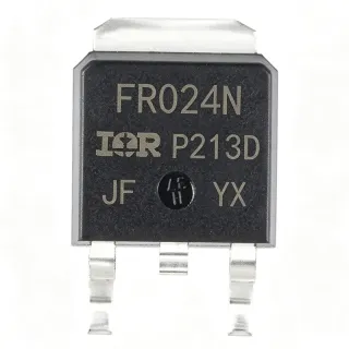
IRFR3411TRPBF - 100V 32A N-Channel HEXFET MOSFET | Infineon
부품 번호: IRFR3411TRPBF ✓ 활성| 수량 | 단가 | 합계 |
|---|---|---|
| 1 | $1.54 | $1.54 |
| 10 | $1.36 | $13.60 |
| 100 | $1.08 | $108.00 |
| 500 | $0.86 | $430.00 |
| 1,000 | $0.7 | $700.00 |
| 2,500 | $0.55 | $1,375.00 |
IRFR3411TRPBF 개요
Key specifications include V(BR)DSS of 100V, RDS(on) max of 44 mOhm, gate charge of 48 nC, and a maximum junction temperature of 175C enabling reliable operation in thermally demanding environments. The device features dynamic dv/dt rating, fast switching speed, and full avalanche rated ruggedness, making it suitable for switching power supply designs that encounter inductive load transients.
The IRFR3411TRPBF utilizes Infineon's HEXFET Power MOSFET technology, leveraging advanced process techniques to achieve extremely low on-resistance per silicon area while maintaining fast switching characteristics. The combination of low RDS(on), high continuous current capability, and avalanche ruggedness provides high efficiency and reliability across demanding power conversion topologies.
Typical applications include DC-DC converters, synchronous rectification in switched-mode power supplies (SMPS), motor drive circuits, and solenoid/relay drivers. The TO-252AA (DPAK) surface-mount package enables automated PCB assembly while providing sufficient thermal performance for medium-power applications up to approximately 130W with proper PCB copper area.
When designing with this device, ensure adequate thermal management - calculate power dissipation as P = I^2 x RDS(on) and verify junction temperature stays below 175C using the package's thermal resistance and the application's copper area. A gate drive voltage of 10V is recommended for full RDS(on) specification; lower gate voltages significantly increase conduction losses.
드롭인 대체품: IRFR3411TRPBF — 동일 패키지, 핀 호환. PCB 재작업이 필요한 다른 패키지 부품은 제외됩니다.
이 시리즈의 변형
다음과 드롭인 호환되는 동일 시리즈 모델: IRFR3411TRPBF (동일 폼 팩터 및 풋프린트) — 차이점: Technology, Package, RoHS Status, FET Type, Operating Temperature Range.
빠른 비교 도구 — 나란히 비교할 대체 부품을 선택하십시오:
IRFR3411PBF
✅ 드롭인📋 참조 대체품 (카탈로그에 없음)
IRFR3710ZTRPBF
✅ 드롭인✓ 재고 있음
$0.42 / 개
데이터시트 보기 →IRFR4510
✅ 드롭인📋 참조 대체품 (카탈로그에 없음)
IRFR220NTRPBF
✅ 드롭인 ⚠️ 사양 미검증✓ 재고 있음
$0.22 / 개
데이터시트 보기 →IRFZ34NPBF
✅ 드롭인✓ 재고 있음
$0.61 / 개
데이터시트 보기 →IRFB4110PBF
✅ 드롭인✓ 재고 있음
$1.55 / 개
데이터시트 보기 →VBE1104N
✅ 드롭인📋 참조 대체품 (카탈로그에 없음)
IRFR3411TRPBF 최대 정격 & 전기적 특성
| Polarity | N-Channel |
| FET Type | MOSFET (Metal Oxide) |
| V(BR)DSS (Drain-Source Breakdown Voltage) | 100 V |
| RDS(on) max @ VGS=10V | 44 mOhm |
| Continuous Drain Current (Id) @ Tc | 32 A |
| Power Dissipation (Pd) @ Tc | 130 W |
| Gate Charge (Qg) | 48 nC |
| Operating Mode | Enhancement |
| Maximum Junction Temperature | 175 C |
| 동작 온도 범위 | -55 C to +175 C |
| 패키지 | TO-252AA (DPAK) |
| 실장 유형 | Surface Mount |
| 핀 수 | 3 |
| Technology | HEXFET Power MOSFET (IR) |
| Avalanche Rated | Yes (fully avalanche rated) |
| dv/dt Rating | Dynamic dv/dt rated |
| Lead-Free / RoHS | Yes (Lead-free, PBF suffix) |
IRFR3411TRPBF 핀 구성
| 핀 1 | Gate — MOSFET gate control input (drive with 10V for full enhancement) |
| 핀 2 | Drain — MOSFET drain; connected to metal tab/back of package for thermal dissipation |
| 핀 3 | Source — MOSFET source; reference for gate drive and main current return |
안전 동작 영역 (DC)
일반적인 애플리케이션
IRFR3411TRPBF 적합 용도: 6 애플리케이션s: Synchronous Rectification in SMPS, DC-DC Buck Converters (12V to 3.3V/5V rails), Motor Drive and H-Bridge Circuits, Solenoid and Relay Drivers, Automotive 12V/24V Load Switching, Solar Charge Controller Switching.
Synchronous Rectification in SMPS
The IRFR3411TRPBF serves as the low-side synchronous rectifier in forward, half-bridge, and full-bridge SMPS topologies delivering 100W to 500W. Its 44 mOhm RDS(on) at VGS=10V keeps conduction losses below 5W at 10A output, while the 48 nC gate charge enables clean switching at 100-300 kHz with moderate driver losses. The 32A continuous Id rating provides ample margin for transient inductor currents, and the DPAK footprint simplifies PCB layout compared to D2PAK alternatives. Designers should drive the gate with a dedicated low-impedance driver to fully enhance the MOSFET within the dead-time window and minimize body-diode conduction.
추천
DC-DC Buck Converters (12V to 3.3V/5V rails)
The IRFR3411TRPBF is well suited as the main switch or synchronous FET in non-isolated buck converters for distributed power architectures. Operating from 12V or 24V input rails, its 100V V(BR)DSS rating provides 4x safety margin on 24V industrial buses. The 32A continuous drain current at Tc supports 10-15A continuous loads with proper PCB copper area, and the 175C maximum junction temperature enables operation in thermally enclosed enclosures. The TO-252AA package is preferred for cost-sensitive designs where D2PAK thermal performance is not required.
추천
Motor Drive and H-Bridge Circuits
The IRFR3411TRPBF functions as one of four switches in a brushed DC motor H-bridge or as the low-side switch in three-phase brushless DC (BLDC) motor drives up to 200W. Its avalanche rating and 175C junction temperature allow operation through motor back-EMF transients and inductive kick events. With 32A continuous current capability, it can drive motors drawing up to 15-20A continuous with adequate PCB thermal design. Designers should add gate-source resistors (10-100 kOhm) to prevent inadvertent turn-on from dv/dt coupling in half-bridge configurations.
추천
Solenoid and Relay Drivers
The IRFR3411TRPBF drives 12V/24V solenoids, relays, and contactor coils in industrial control and automotive applications. With 100V V(BR)DSS, it can withstand flyback voltages from 24V inductive loads with proper freewheeling diode placement. The 32A continuous drain current supports most industrial solenoids up to 5A continuous, and the avalanche rating handles unclamped inductive turn-off transients if a flyback diode is missing or fails. The DPAK package suits both PCB-mounted driver stages and module-level integration.
추천
Automotive 12V/24V Load Switching
The IRFR3411TRPBF is suitable for automotive 12V and 24V body electronics, lighting, and accessory switching where its 100V V(BR)DSS rating provides margin against 24V jump-start and 48V load-dump transients. While not AEC-Q100 qualified, its 175C maximum junction temperature and ruggedized HEXFET construction meet automotive environmental demands for underhood and non-safety applications. The DPAK package withstands automotive thermal cycling and vibration when properly soldered with adequate PCB staking.
추천
Solar Charge Controller Switching
The IRFR3411TRPBF serves as the main switching element in PWM solar charge controllers for off-grid photovoltaic systems operating from 12V to 48V battery banks. Its 100V V(BR)DSS rating accommodates 24V and 48V battery systems with surge margin, and the 32A current capability supports charge currents up to 20-25A. The low RDS(on) minimizes heat dissipation during PWM switching, while the avalanche rating handles the inductive transients from long PV wire runs. For higher efficiency MPPT designs, designers can pair this FET with a synchronous rectifier stage.
추천
추천 제품 요약
엔지니어링 참조 데이터: IRFR3411TRPBF — 비교, 설계 지침 및 규정 준수 정보.
선택 가이드
대체품과의 비교
| 파라미터 | 이 제품 | IRFR3411PBF | IRFR3710Z | IRFR4510 | VBE1104N | IRFZ34NPBF |
|---|---|---|---|---|---|---|
| Package | TO-252AA (DPAK) | TO-252AA (DPAK) - same | TO-252AA (DPAK) - same | TO-252AA (DPAK) - same | TO-252AA (DPAK) - same | TO-220AB - different |
| Brand | Infineon | Infineon - same | Infineon - same | Infineon - same | VBsemi - cross-brand | Infineon - same |
| V(BR)DSS | 100 V | 100 V | 100 V | 100 V | 100 V | 55 V |
주요 차별점
- Higher current rating vs IRFR3710Z-class alternatives (vs Standard DPAK 100V N-channel MOSFETs)
- Fully avalanche-rated for ruggedness (vs Non-avalanche-rated 100V DPAK MOSFETs)
- Surface-mount DPAK vs through-hole TO-220 alternatives (vs TO-220 packaged MOSFETs like IRFZ34N)
설계 노트
The TO-252AA (DPAK) package relies on PCB copper area for heat dissipation. For continuous operation at 10A load, ensure at least 1 square inch of copper pour on the drain tab land pattern to keep junction temperature below 150C. Without adequate copper, RthJA exceeds 80 C/W and continuous drain current must be derated below 5A. For high-power designs, use multiple thermal vias under the drain pad to conduct heat to inner PCB layers.
Layout the gate drive loop as small as possible to minimize parasitic inductance and ringing. Keep the gate series resistor (typically 10-33 Ohm) close to the gate pin. Place a 100 kOhm gate-source resistor to prevent inadvertent turn-on from dv/dt coupling in half-bridge configurations. The drain tab should be soldered to a generous copper pour that doubles as both electrical connection and heatsink.
Do not exceed V(BR)DSS=100V under any transient condition including avalanche from unclamped inductive loads - add a freewheeling diode across inductive loads to prevent drain voltage overshoot. Ensure gate-source voltage never exceeds +/-20V absolute maximum; static electricity during handling can exceed this - follow ESD precautions. Below VGS=10V, RDS(on) increases dramatically causing unexpected heat; use a proper gate driver rather than direct logic-level drive.
In switching applications at frequencies above 100 kHz, the gate charge (Qg=48 nC) demands substantial driver current: peak gate current = Qg * switching frequency. A dedicated gate driver IC such as IRS21064 or discrete push-pull driver with at least 1A peak sink/source capability is recommended. Without sufficient gate drive current, switching losses rise and the MOSFET may operate in the linear region during transitions, causing severe heating.
규정 준수 정보
PBF suffix indicates lead-free matte-tin plating, fully RoHS compliant per EU Directive 2011/65/EU. Device is not AEC-Q100 qualified - for automotive safety applications, use AEC-Q100 qualified parts. REACH compliant per Infineon product declaration.