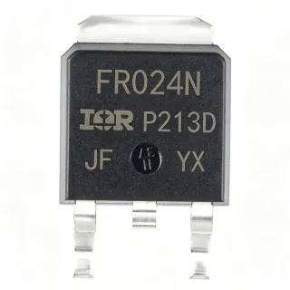
IRFR3411TRPBF - 100V 32A N-Channel HEXFET MOSFET | Infineon
MPN: IRFR3411TRPBF ✓ Active| Qty | Unit Price | Extended |
|---|---|---|
| 1 | $1.54 | $1.54 |
| 10 | $1.36 | $13.60 |
| 100 | $1.08 | $108.00 |
| 500 | $0.86 | $430.00 |
| 1,000 | $0.7 | $700.00 |
| 2,500 | $0.55 | $1,375.00 |
Drop-in alternatives for IRFR3411TRPBF — same package, pin-to-pin compatible. Different-package parts requiring PCB rework are excluded.
Quick Comparison Tool — Select alternative parts for side-by-side comparison:
IRFR3411PBF
✅ Drop-In📋 Reference alternative (not in catalog)
IRFR3710ZTRPBF
✅ Drop-In✓ In Stock
$0.42 / Unit
View Datasheet →IRFR4510
✅ Drop-In📋 Reference alternative (not in catalog)
IRFR220NTRPBF
✅ Drop-In ⚠️ 参数待验证✓ In Stock
$0.22 / Unit
View Datasheet →IRFZ34NPBF
✅ Drop-In✓ In Stock
$0.61 / Unit
View Datasheet →IRFB4110PBF
✅ Drop-In✓ In Stock
$1.55 / Unit
View Datasheet →VBE1104N
✅ Drop-In📋 Reference alternative (not in catalog)
IRFR3411TRPBF Maximum Ratings & Electrical Characteristics
| Polarity | N-Channel |
| FET Type | MOSFET (Metal Oxide) |
| V(BR)DSS (Drain-Source Breakdown Voltage) | 100 V |
| RDS(on) max @ VGS=10V | 44 mOhm |
| Continuous Drain Current (Id) @ Tc | 32 A |
| Power Dissipation (Pd) @ Tc | 130 W |
| Gate Charge (Qg) | 48 nC |
| Operating Mode | Enhancement |
| Maximum Junction Temperature | 175 C |
| Operating Temperature Range | -55 C to +175 C |
| Package | TO-252AA (DPAK) |
| Mounting Type | Surface Mount |
| Number of Pins | 3 |
| Technology | HEXFET Power MOSFET (IR) |
| Avalanche Rated | Yes (fully avalanche rated) |
| dv/dt Rating | Dynamic dv/dt rated |
| Lead-Free / RoHS | Yes (Lead-free, PBF suffix) |
IRFR3411TRPBF Pin Configuration
| Pin 1 | Gate — MOSFET gate control input (drive with 10V for full enhancement) |
| Pin 2 | Drain — MOSFET drain; connected to metal tab/back of package for thermal dissipation |
| Pin 3 | Source — MOSFET source; reference for gate drive and main current return |
Safe Operating Area (DC)
Typical Applications
IRFR3411TRPBF is suitable for 6 applications: Synchronous Rectification in SMPS, DC-DC Buck Converters (12V to 3.3V/5V rails), Motor Drive and H-Bridge Circuits, Solenoid and Relay Drivers, Automotive 12V/24V Load Switching, Solar Charge Controller Switching.
Synchronous Rectification in SMPS
The IRFR3411TRPBF serves as the low-side synchronous rectifier in forward, half-bridge, and full-bridge SMPS topologies delivering 100W to 500W. Its 44 mOhm RDS(on) at VGS=10V keeps conduction losses below 5W at 10A output, while the 48 nC gate charge enables clean switching at 100-300 kHz with moderate driver losses. The 32A continuous Id rating provides ample margin for transient inductor currents, and the DPAK footprint simplifies PCB layout compared to D2PAK alternatives. Designers should drive the gate with a dedicated low-impedance driver to fully enhance the MOSFET within the dead-time window and minimize body-diode conduction.
Recommended
DC-DC Buck Converters (12V to 3.3V/5V rails)
The IRFR3411TRPBF is well suited as the main switch or synchronous FET in non-isolated buck converters for distributed power architectures. Operating from 12V or 24V input rails, its 100V V(BR)DSS rating provides 4x safety margin on 24V industrial buses. The 32A continuous drain current at Tc supports 10-15A continuous loads with proper PCB copper area, and the 175C maximum junction temperature enables operation in thermally enclosed enclosures. The TO-252AA package is preferred for cost-sensitive designs where D2PAK thermal performance is not required.
Recommended
Motor Drive and H-Bridge Circuits
The IRFR3411TRPBF functions as one of four switches in a brushed DC motor H-bridge or as the low-side switch in three-phase brushless DC (BLDC) motor drives up to 200W. Its avalanche rating and 175C junction temperature allow operation through motor back-EMF transients and inductive kick events. With 32A continuous current capability, it can drive motors drawing up to 15-20A continuous with adequate PCB thermal design. Designers should add gate-source resistors (10-100 kOhm) to prevent inadvertent turn-on from dv/dt coupling in half-bridge configurations.
Recommended
Solenoid and Relay Drivers
The IRFR3411TRPBF drives 12V/24V solenoids, relays, and contactor coils in industrial control and automotive applications. With 100V V(BR)DSS, it can withstand flyback voltages from 24V inductive loads with proper freewheeling diode placement. The 32A continuous drain current supports most industrial solenoids up to 5A continuous, and the avalanche rating handles unclamped inductive turn-off transients if a flyback diode is missing or fails. The DPAK package suits both PCB-mounted driver stages and module-level integration.
Recommended
Automotive 12V/24V Load Switching
The IRFR3411TRPBF is suitable for automotive 12V and 24V body electronics, lighting, and accessory switching where its 100V V(BR)DSS rating provides margin against 24V jump-start and 48V load-dump transients. While not AEC-Q100 qualified, its 175C maximum junction temperature and ruggedized HEXFET construction meet automotive environmental demands for underhood and non-safety applications. The DPAK package withstands automotive thermal cycling and vibration when properly soldered with adequate PCB staking.
Recommended
Solar Charge Controller Switching
The IRFR3411TRPBF serves as the main switching element in PWM solar charge controllers for off-grid photovoltaic systems operating from 12V to 48V battery banks. Its 100V V(BR)DSS rating accommodates 24V and 48V battery systems with surge margin, and the 32A current capability supports charge currents up to 20-25A. The low RDS(on) minimizes heat dissipation during PWM switching, while the avalanche rating handles the inductive transients from long PV wire runs. For higher efficiency MPPT designs, designers can pair this FET with a synchronous rectifier stage.
Recommended
Recommended Products Summary
Engineering reference data for IRFR3411TRPBF — comparison, design guidance, and compliance information.
Selection Guide
Comparison with Alternatives
| Parameter | This Product | IRFR3411PBF | IRFR3710Z | IRFR4510 | VBE1104N | IRFZ34NPBF |
|---|---|---|---|---|---|---|
| Package | TO-252AA (DPAK) | TO-252AA (DPAK) - same | TO-252AA (DPAK) - same | TO-252AA (DPAK) - same | TO-252AA (DPAK) - same | TO-220AB - different |
| Brand | Infineon | Infineon - same | Infineon - same | Infineon - same | VBsemi - cross-brand | Infineon - same |
| V(BR)DSS | 100 V | 100 V | 100 V | 100 V | 100 V | 55 V |
| Continuous Drain Current (Id) | 32 A | 32 A | 56 A | 30 A | [DATA_NEEDED] | 26 A |
| RDS(on) max @ VGS=10V | 44 mOhm | 44 mOhm | 25 mOhm | 22 mOhm | [DATA_NEEDED] | 40 mOhm |
| Gate Charge (Qg) | 48 nC | 48 nC | [DATA_NEEDED] | [DATA_NEEDED] | [DATA_NEEDED] | [DATA_NEEDED] |
| Power Dissipation (Tc) | 130 W | 130 W | [DATA_NEEDED] | [DATA_NEEDED] | [DATA_NEEDED] | 68 W |
| Avalanche Rated | Yes | Yes | [DATA_NEEDED] | [DATA_NEEDED] | [DATA_NEEDED] | Yes |
Key Differentiators
- Higher current rating vs IRFR3710Z-class alternatives (vs Standard DPAK 100V N-channel MOSFETs)
- Fully avalanche-rated for ruggedness (vs Non-avalanche-rated 100V DPAK MOSFETs)
- Surface-mount DPAK vs through-hole TO-220 alternatives (vs TO-220 packaged MOSFETs like IRFZ34N)
Design Notes
The TO-252AA (DPAK) package relies on PCB copper area for heat dissipation. For continuous operation at 10A load, ensure at least 1 square inch of copper pour on the drain tab land pattern to keep junction temperature below 150C. Without adequate copper, RthJA exceeds 80 C/W and continuous drain current must be derated below 5A. For high-power designs, use multiple thermal vias under the drain pad to conduct heat to inner PCB layers.
Layout the gate drive loop as small as possible to minimize parasitic inductance and ringing. Keep the gate series resistor (typically 10-33 Ohm) close to the gate pin. Place a 100 kOhm gate-source resistor to prevent inadvertent turn-on from dv/dt coupling in half-bridge configurations. The drain tab should be soldered to a generous copper pour that doubles as both electrical connection and heatsink.
Do not exceed V(BR)DSS=100V under any transient condition including avalanche from unclamped inductive loads - add a freewheeling diode across inductive loads to prevent drain voltage overshoot. Ensure gate-source voltage never exceeds +/-20V absolute maximum; static electricity during handling can exceed this - follow ESD precautions. Below VGS=10V, RDS(on) increases dramatically causing unexpected heat; use a proper gate driver rather than direct logic-level drive.
In switching applications at frequencies above 100 kHz, the gate charge (Qg=48 nC) demands substantial driver current: peak gate current = Qg * switching frequency. A dedicated gate driver IC such as IRS21064 or discrete push-pull driver with at least 1A peak sink/source capability is recommended. Without sufficient gate drive current, switching losses rise and the MOSFET may operate in the linear region during transitions, causing severe heating.
Compliance Information
PBF suffix indicates lead-free matte-tin plating, fully RoHS compliant per EU Directive 2011/65/EU. Device is not AEC-Q100 qualified - for automotive safety applications, use AEC-Q100 qualified parts. REACH compliant per Infineon product declaration.