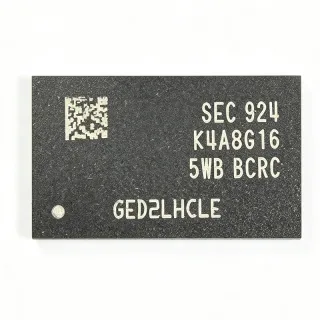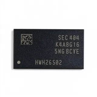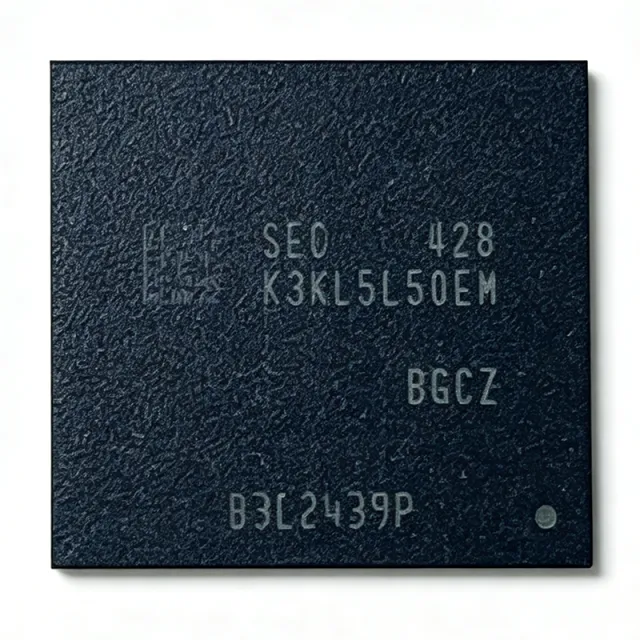
K3KL4L40EM-BGCU - 12GB LPDDR5X DRAM 8533Mbps | Samsung
부품 번호: K3KL4L40EM-BGCU ✓ 활성| 수량 | 단가 | 합계 |
|---|---|---|
| 1 | $135 | $135.00 |
| 10 | $97.5 | $975.00 |
| 100 | $86.25 | $8,625.00 |
| 500 | $82.5 | $41,250.00 |
| 1,000 | $78.75 | $78,750.00 |
K3KL4L40EM-BGCU 개요
LPDDR5X (Low Power Double Data Rate 5X) is an extension of the JEDEC LPDDR5 standard that pushes the data rate ceiling beyond LPDDR5's 6,400 Mbps while lowering supply voltage for reduced power consumption. As a class of volatile memory in the DRAM hierarchy, LPDDR5X serves as the main system memory in mobile SoC platforms, sitting alongside application processors such as Qualcomm Snapdragon and MediaTek Dimensity where bandwidth-per-watt is the dominant design metric.
Key features of the K3KL4L40EM-BGCU include its 96 Gbit density (single-die 12 GB organization), an x64 bus width, and an industry-leading 8,533 Mbps maximum data rate. The ultra-low-power mobile DRAM design targets energy efficiency, which directly extends battery life in handheld and wearable products. The 496-ball FBGA (Fine-Pitch Ball Grid Array) package provides a compact footprint for dense mobile PCBs.
Architecturally, the device belongs to Samsung's LPDDR5X family alongside the 64 Gbit K3KL3L30DM-BGCU and 128 Gbit K3KL5L50DM-BGCU, all sharing the same 496 FBGA footprint and 8,533 Mbps speed grade. This density-family structure allows platform vendors to scale memory capacity between 8 GB, 12 GB, and 16 GB total configurations (with stacked or multi-die assemblies) without changing PCB layout or signal-integrity design.
Typical applications include flagship smartphones paired with Snapdragon-class CPUs, tablets, wearables, and edge-AI computing modules where high memory bandwidth is needed for on-device inference.
Design consideration: LPDDR5X signal integrity at 8,533 Mbps demands strict length-matched routing, controlled impedance, and following the SoC vendor's reference layout guidelines.
This page synthesizes distributor stock data, drop-in density alternatives, and practical design notes not found in the manufacturer datasheet. Pricing and stock references are as of 2026-09-04.
드롭인 대체품: K3KL4L40EM-BGCU — 동일 패키지, 핀 호환. PCB 재작업이 필요한 다른 패키지 부품은 제외됩니다.
이 시리즈의 변형
다음과 드롭인 호환되는 동일 시리즈 모델: K3KL4L40EM-BGCU (동일 폼 팩터 및 풋프린트) — 차이점: Density, Interface, Data Rate, Memory Type, Mounting Type.
빠른 비교 도구 — 나란히 비교할 대체 부품을 선택하십시오:
K3KL3L30DM-BGCU
✓ 재고 있음
$45.9375 / 개
데이터시트 보기 →K3KL5L50DM-BGCU
✓ 재고 있음
가격 문의
데이터시트 보기 →K3KL7L70EM-MGCU
✓ 재고 있음
$12 / 개
데이터시트 보기 →K3KL8L80DM-MGCU
✓ 재고 있음
가격 문의
데이터시트 보기 →K3KL4L40DM-BGCU
📋 참조 대체품 (카탈로그에 없음)
K3KL4L40EM-BGCU 최대 정격 & 전기적 특성
| 메모리 유형 | LPDDR5X DRAM |
| Density | 96 Gbit (12 GB) |
| 메모리 구성 | x64 |
| 데이터 속도 | 8533 Mbps |
| 인터페이스 | LPDDR5X (LPDDR5 JEDEC-based) |
| 패키지 | 496-ball FBGA |
| 실장 유형 | Surface Mount |
| Application | Tablet, Smartphone, Wearable Devices |
| Product Family | Samsung LPDDR5X (K3KL4L40EM series) |
| Companion Densities | 64 Gbit (K3KL3L30DM-BGCU), 128 Gbit (K3KL5L50DM-BGCU) |
| Power Characteristic | Ultra-low-power mobile DRAM |
| RoHS 상태 | unknown |
| Ball Count | 496 |
| Storage Class | Volatile memory (DRAM) |
K3KL4L40EM-BGCU 496-ball fbga 핀 구성 가이드
K3KL4L40EM-BGCU(496-ball fbga 패키지)의 핀 구성입니다. 이 디지털 IC에는 GPIO, 통신 인터페이스(UART, SPI, I2C), 전원 핀이 포함되어 있습니다. 대체 핀 기능과 구성 옵션은 제조사 데이터시트를 참조하십시오. 임베디드 시스템 설계와 PCB 레이아웃에 필수적입니다.

다음에 대한 상세 핀아웃 데이터 없음: K3KL4L40EM-BGCU.
다음을 참조하십시오: 데이터시트 전체 핀 구성은 다음을 참조하십시오.
일반적인 애플리케이션
K3KL4L40EM-BGCU 적합 용도: 6 애플리케이션s: Flagship Smartphone Main Memory, Tablet Main Memory, Wearable and Smart Devices, Edge AI and On-Device Inference, Automotive Cockpit and ADAS Compute Modules, High-Performance Embedded Computing Modules.
Flagship Smartphone Main Memory
The K3KL4L40EM-BGCU is purpose-built as main system memory for flagship smartphones, where its 8,533 Mbps data rate provides the bandwidth headroom required by Qualcomm Snapdragon and MediaTek Dimensity application processors with on-device AI acceleration. Its 96 Gbit (12 GB) density allows a two-package design to reach 24 GB, supporting heavy multitasking and large AI model residency in memory. As ultra-low-power LPDDR5X, it reduces memory subsystem energy per bit transferred, directly extending battery life versus LPDDR5 at equivalent bandwidth. The 496-ball FBGA footprint fits standard mobile PCB PoP-adjacent layouts, and shared footprint across the 64/96/128 Gbit family lets one platform design scale across memory tiers without respin, provided the SoC memory-compatibility list covers the chosen density.
추천
Tablet Main Memory
Tablets benefit from the K3KL4L40EM-BGCU's combination of high bandwidth and low power, since they run large-display rendering pipelines, split-screen multitasking, and increasingly on-device AI assistants. The 8,533 Mbps LPDDR5X interface supplies the sustained bandwidth needed to drive high-resolution displays and GPU workloads without the memory subsystem becoming the bottleneck, while the ultra-low-power design keeps thermals within the passive-cooling envelope typical of tablets. At 12 GB per device, a single package can serve mid-range tablet configurations, and two packages reach 24 GB for productivity-oriented models. Because Samsung's LPDDR5X family shares the 496-ball FBGA footprint across densities, tablet platforms can offer multiple memory SKUs from a single PCB layout, shortening qualification cycles and reducing inventory complexity across the product line.
추천
Wearable and Smart Devices
Samsung explicitly lists wearable devices among the target applications of its LPDDR5X lineup, and the K3KL4L40EM-BGCU's ultra-low-power mobile DRAM design addresses the strict energy budgets of smartwatches, AR glasses, and smart rings with advanced compute. LPDDR5X's reduced operating voltage and high efficiency deliver bandwidth-per-milliwatt that legacy LPDDR4X cannot match, which matters for wearables running compact on-device AI models for health sensing and voice assistance. Designers of very space-constrained wearables should evaluate whether the 64 Gbit K3KL3L30DM-BGCU in the same 496-ball FBGA footprint better matches their capacity and cost targets, since the footprint is common across the family. Signal integrity at 8,533 Mbps requires adherence to the SoC vendor's reference routing for the short point-to-point LPDDR5X links typical in wearable form factors.
추천
Edge AI and On-Device Inference
On-device generative AI and computer-vision inference are memory-bandwidth-bound workloads, making the K3KL4L40EM-BGCU's 8,533 Mbps data rate a direct enabler: higher bandwidth translates to higher tokens-per-second and frames-per-second for NPUs integrated in Snapdragon and Dimensity platforms. The 12 GB capacity allows larger quantized models to remain resident in DRAM, avoiding costly swaps to storage. Samsung's LPDDR5X family is positioned precisely for this AI-at-the-edge use case, with the industry-leading speed grade minimizing latency for memory-intensive transformer inference. The ultra-low-power profile also keeps sustained-inference thermals manageable in fanless devices. When model sizes vary across product tiers, the footprint-compatible 96/128 Gbit family members let AI product lines scale memory capacity while reusing a single validated LPDDR5X layout and memory-training configuration.
추천
Automotive Cockpit and ADAS Compute Modules
High-performance automotive cockpit processors and ADAS domains increasingly specify LPDDR5X-class memory for AI-assisted driver monitoring, surround-view rendering, and infotainment. The K3KL4L40EM-BGCU's 8,533 Mbps bandwidth supports the multi-display, multi-camera workloads of digital cockpit SoCs, while its low power helps meet the thermal constraints of passively-cooled head units. Twelve gigabytes per package enables multi-OS (instrument cluster plus infotainment) virtualized platforms on a single SoC. Note that the standard consumer part must be evaluated against the project's AEC-Q100 requirements; Samsung offers automotive-qualified LPDDR variants, and designers should confirm qualification grade for their specific program before using this mobile-grade component. The 496-ball FBGA footprint and density-family structure simplify qualification across cockpit trim levels with differing memory configurations.
추천
High-Performance Embedded Computing Modules
Embedded computing modules - SoMs, COM Express alternatives built on mobile-class Qualcomm or MediaTek SoCs - adopt LPDDR5X like the K3KL4L40EM-BGCU to deliver smartphone-level memory performance in industrial edge gateways, robotics controllers, and vision systems. The 8,533 Mbps rate supplies the bandwidth for multi-camera sensor fusion and real-time analytics, and the ultra-low-power design suits fanless enclosures where every watt of dissipation matters. Soldered-down DRAM also improves vibration reliability versus SODIMM-based designs, a key requirement in mobile robotics and transportation. Because the module integrator controls the LPDDR5X layout, using Samsung's footprint-stable 496-ball FBGA family simplifies second-sourcing across densities within one carrier-board and module roadmap. Verify controller training data and compatibility lists for the exact Samsung part number before production release.
추천
추천 제품 요약
엔지니어링 참조 데이터: K3KL4L40EM-BGCU — 비교, 설계 지침 및 규정 준수 정보.
선택 가이드
대체품과의 비교
| 파라미터 | 이 제품 | K3KL4L40DM-BGCU | K3KL3L30DM-BGCU | K3KL5L50DM-BGCU | K3KL7L70EM-MGCU |
|---|---|---|---|---|---|
| Package | 496-ball FBGA | 496-ball FBGA - same | 496-ball FBGA - same | 496-ball FBGA - same | 496-ball FBGA - same |
| Brand | Samsung | Samsung | Samsung | Samsung | Samsung |
| Data Rate | 8533 Mbps | 8533 Mbps | 8533 Mbps | 8533 Mbps | 8533 Mbps |
| Memory Technology | LPDDR5X | LPDDR5X | LPDDR5X | LPDDR5X | LPDDR5X |
| Primary Application | Tablet, Smartphone, Wearable | Mobile DRAM (same family) | Tablet, Smartphone, Wearable | Tablet, Smartphone, Wearable | Mobile DRAM (same family) |
| Generation Suffix | EM (newest) | DM (prior generation) | DM | DM | EM (current) |
주요 차별점
- Newest EM generation of the 96 Gbit LPDDR5X family (vs K3KL4L40DM-BGCU)
- Maximum density per package within footprint-compatible family (vs K3KL3L30DM-BGCU)
- Industry-leading 8,533 Mbps speed grade (vs LPDDR5-class memory (e.g., K4AAG165WM DDR4/LPDDR5 alternatives))
설계 노트
At 8,533 Mbps, LPDDR5X signal integrity dominates design success. Keep all data, address, and command traces length-matched within the SoC vendor's specification (typically on the order of a few mils within byte lanes), maintain controlled single-ended and differential impedance, and reference signals to solid ground planes. Follow the Qualcomm or MediaTek reference design layout for the specific SoC, as LPDDR5X training margins are validated only against those layouts. Avoid routing LPDDR5X lines across plane splits and minimize via transitions on data groups.
Verify SoC compatibility before substitution. LPDDR5X devices are not freely interchangeable: the memory controller must include the Samsung device's timings and training configuration in its supported-memory list. The 96 Gbit EM-generation part and the 96 Gbit DM-generation K3KL4L40DM-BGCU share footprint and specs, but die-revision differences can require updated firmware training tables. Always confirm the exact MPN against the SoC vendor's memory compatibility (QVL) documentation before committing the BOM, and lock the die revision on incoming inspection.
LPDDR5X operates at reduced supply voltages relative to LPDDR5 to achieve its power-efficiency targets; use the PMIC rail specifically designed for LPDDR5X VDD1/VDD2/VDDQ domains with the sequencing order required by the SoC platform. Decouple each supply domain per the Samsung datasheet layout guidance with low-ESR ceramics placed close to the ball-field vias. Power-rail ripple on VDDQ directly degrades eye margins at 8,533 Mbps, so measure rail noise during memory training validation rather than assuming margin.
The 496-ball FBGA requires a fine-pitch land pattern per the Samsung package drawing; use NSMD pads and solder-mask-defined openings only where the land-pattern note permits. Because Samsung's LPDDR5X density family (64/96/128 Gbit) shares this footprint, design the PCB to accept any family member: populate all balls per the drawing, avoid hard-wiring density-specific balls, and validate the layout with both the target density and its neighbors during SI simulation to enable tiered SKU strategies without respin.
규정 준수 정보
Compliance status not stated in the provided web data; confirm RoHS/REACH declarations via Samsung Semiconductor's official environmental documentation for this MPN.