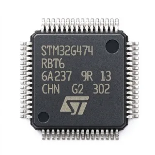
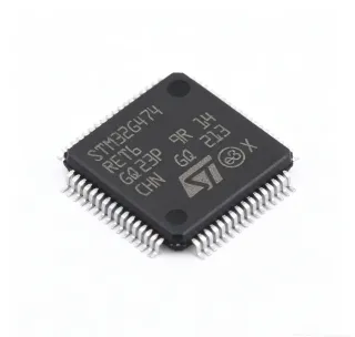
STM32F030R - Cortex-M0 48MHz MCU, 64KB Flash, 64-LQFP | ST
부품 번호: STM32F030R ✓ 활성| 수량 | 단가 | 합계 |
|---|---|---|
| 1 | $1.85 | $1.85 |
| 10 | $1.62 | $16.20 |
| 100 | $1.28 | $128.00 |
| 500 | $1.05 | $525.00 |
| 1,000 | $0.88 | $880.00 |
| 3,000 | $0.74 | $2,220.00 |
STM32F030R 개요
A microcontroller (MCU) is a single-chip computer that integrates a processor core, memory (Flash for code, SRAM for data), and a rich set of programmable peripherals on a single die. The Cortex-M0 is the smallest and most energy-efficient member of the ARM Cortex-M processor family, designed for cost-sensitive, deterministic embedded applications. Within the ST portfolio, the STM32F0 sits below the Cortex-M3/M4 STM32F1/F3 lines and above the 8-bit STM8, occupying the mainstream 32-bit entry point. The STM32F030 specifically targets cost-down designs that previously used 8/16-bit MCUs but now require 32-bit performance, USB-less connectivity, and ST's strong STM32 tool ecosystem (CubeMX, HAL, Standard Peripheral Library).
Key features include a 12-bit 1 MSPS ADC with up to 16 channels, multiple 16-bit and 32-bit timers (including PWM, input capture, and quadrature encoder support), two I2C, two SPI (one I2S-capable), one USB 2.0 Full-Speed (device mode, on R8/C0/C8/CB parts), one CAN 2.0B (RC0/RC8 variants), and up to 55 GPIO. An integrated 8 MHz HSI RC oscillator with 1% accuracy and a 40 kHz LSI reduce external component count. The 64-LQFP package provides 64 pins at 10 mm x 10 mm body, including dedicated pins for BOOT0, NRST, OSC_IN/OSC_OUT, and full SWD debug.
The architecture pairs a 3-stage pipeline Cortex-M0 core with a 32-bit AHB-Lite bus and a multi-channel DMA controller. The Nested Vectored Interrupt Controller (NVIC) handles up to 32 maskable interrupts with deterministic 16-cycle latency. A cyclic redundancy check (CRC) peripheral, two watchdogs (IWDG/WWDG), and a 7-channel DMA accelerate data movement without CPU overhead.
Typical applications include consumer appliances (washing machines, induction cookers), industrial sensor hubs, USB HID peripherals, low-cost CAN nodes, smart meters, and home automation. The compact LQFP-64 footprint and 48 MHz clock headroom make it a common choice for migration paths from 8-bit PIC/AVR designs into the STM32 ecosystem.
When designing with the STM32F030R, ensure each VDD/VDDA pin pair has a 100 nF decoupling capacitor placed within 2 mm of the pin, and consider the BOOT0 strap resistor for boot mode selection. The 64-LQFP package has limited thermal headroom at high ambient temperatures, so verify junction temperature under worst-case load.
This page synthesizes distributor pricing, drop-in pin-compatible alternatives, application companion parts, and practical design notes drawn from multiple sources, including the official ST datasheet, DigiKey listings, and ST community resources - not found in any single source.
드롭인 대체품: STM32F030R — 동일 패키지, 핀 호환. PCB 재작업이 필요한 다른 패키지 부품은 제외됩니다.
이 시리즈의 변형
다음과 드롭인 호환되는 동일 시리즈 모델: STM32F030R (동일 폼 팩터 및 풋프린트) — 차이점: ADC, Core, Flash Memory, Timers, Package.
빠른 비교 도구 — 나란히 비교할 대체 부품을 선택하십시오:
STM32F051R8T6
✅ 드롭인✓ 재고 있음
$2.45 / 개
데이터시트 보기 →STM32C011R8T6
✅ 드롭인📋 참조 대체품 (카탈로그에 없음)
STM32F030RCT6
✅ 드롭인✓ 재고 있음
$2.25 / 개
데이터시트 보기 →STM32F030R8T6TR
✅ 드롭인📋 참조 대체품 (카탈로그에 없음)
GD32F130R8T6
✅ 드롭인📋 참조 대체품 (카탈로그에 없음)
GD32E230G8U6
✅ 드롭인📋 참조 대체품 (카탈로그에 없음)
STM32F030R 최대 정격 & 전기적 특성
| Core | ARM Cortex-M0 32-bit RISC |
| 최대 클록 주파수 | 48 MHz |
| Flash Memory | 64 KB (R8 variant) |
| SRAM | 8 KB |
| Supply Voltage Range | 2.4 V to 3.6 V |
| 패키지 | 64-pin LQFP (10x10 mm) |
| 동작 온도 | -40C to +85C (industrial, grade 6) |
| ADC | 12-bit, 1 MSPS, up to 16 channels |
| Timers | 1x 16-bit advanced, 5x 16-bit general, 1x 32-bit |
| Communication Interfaces | 2x I2C, 2x SPI (1x I2S), 1x USART, 1x USB FS, 1x CAN |
| GPIO Count | Up to 55 |
| DMA Channels | 7 |
| Internal Oscillator | 8 MHz HSI (+/-1%) + 40 kHz LSI + 32.768 kHz LSE option |
| Debug Interface | Serial Wire Debug (SWD), 2-pin |
| Operating Modes | Run, Sleep, Stop, Standby |
| RoHS 상태 | Compliant |
| MSL 레벨 | 3 (168 hours) |
STM32F030R 핀 구성
| 핀 1 | PC13 — GPIO C13 (Tamper-RTC on some variants) |
| 핀 2 | PC14 — GPIO C14 / OSC32_IN (LSE crystal) |
| 핀 3 | PC15 — GPIO C15 / OSC32_OUT (LSE crystal) |
| 핀 4 | VSS_1 — Ground |
| 핀 5 | VDD_1 — Digital supply voltage (2.4-3.6 V) |
| 핀 6 | OSC_IN — External clock input / HSE crystal |
| 핀 7 | OSC_OUT — External clock output / HSE crystal |
| 핀 8 | NRST — Reset input, active low |
| 핀 9 | VSSA — Analog ground |
| 핀 10 | VDDA — Analog supply voltage |
| 핀 11 | PA0 — GPIO A0 / WKUP / ADC_IN0 / TIM2_CH1 |
| 핀 12 | PA1 — GPIO A1 / ADC_IN1 / TIM2_CH2 |
| 핀 13 | PA2 — GPIO A2 / USART1_TX / ADC_IN2 / TIM2_CH3 |
| 핀 14 | PA3 — GPIO A3 / USART1_RX / ADC_IN3 / TIM2_CH4 |
| 핀 15 | PA4 — GPIO A4 / SPI1_NSS / ADC_IN4 / TIM14_CH1 |
| 핀 16 | PA5 — GPIO A5 / SPI1_SCK / ADC_IN5 |
| 핀 17 | PA6 — GPIO A6 / SPI1_MISO / ADC_IN6 / TIM3_CH1 |
| 핀 18 | PA7 — GPIO A7 / SPI1_MOSI / ADC_IN7 / TIM3_CH2 |
| 핀 19 | PB0 — GPIO B0 / ADC_IN8 / TIM3_CH3 |
| 핀 20 | PB1 — GPIO B1 / ADC_IN9 / TIM3_CH4 |
| 핀 21 | PB2 — GPIO B2 / BOOT1 |
| 핀 22 | PB10 — GPIO B10 / I2C2_SCL / USART3_TX |
| 핀 23 | PB11 — GPIO B11 / I2C2_SDA / USART3_RX |
| 핀 24 | VSS_2 — Ground |
| 핀 25 | VDD_2 — Digital supply voltage |
| 핀 26 | PB12 — GPIO B12 / SPI2_NSS / TIM1_BKIN |
| 핀 27 | PB13 — GPIO B13 / SPI2_SCK / TIM1_CH1N |
| 핀 28 | PB14 — GPIO B14 / SPI2_MISO / TIM1_CH2N |
| 핀 29 | PB15 — GPIO B15 / SPI2_MOSI / TIM1_CH3N |
| 핀 30 | PA8 — GPIO A8 / USART1_CK / TIM1_CH1 / MCO |
| 핀 31 | PA9 — GPIO A9 / USART1_TX / TIM1_CH2 / I2C1_SCL |
| 핀 32 | PA10 — GPIO A10 / USART1_RX / TIM1_CH3 / I2C1_SDA |
| 핀 33 | PA11 — GPIO A11 / USB DM / CAN RX / TIM1_CH4 |
| 핀 34 | PA12 — GPIO A12 / USB DP / CAN TX / TIM1_ETR |
| 핀 35 | PA13 — GPIO A13 / SWDIO |
| 핀 36 | VSS_3 — Ground |
| 핀 37 | VDD_3 — Digital supply voltage |
| 핀 38 | PA14 — GPIO A14 / SWCLK / BOOT0 input during reset |
| 핀 39 | PA15 — GPIO A15 / SPI1_NSS / TIM2_CH1_ETR |
| 핀 40 | PB3 — GPIO B3 / SPI1_SCK / TIM2_CH2 / SWO |
| 핀 41 | PB4 — GPIO B4 / SPI1_MISO / TIM3_CH1 |
| 핀 42 | PB5 — GPIO B5 / SPI1_MOSI / I2C1_SMBA / TIM3_CH2 |
| 핀 43 | PB6 — GPIO B6 / I2C1_SCL / USART1_TX / TIM16_CH1 |
| 핀 44 | PB7 — GPIO B7 / I2C1_SDA / USART1_RX / TIM17_CH1 |
| 핀 45 | BOOT0 — Boot mode selection (must be low for Flash boot) |
| 핀 46 | PB8 — GPIO B8 / TIM16_CH1 / I2C1_SCL / CAN_RX (RC variants) |
| 핀 47 | PB9 — GPIO B9 / TIM17_CH1 / I2C1_SDA / CAN_TX (RC variants) |
| 핀 48 | VSS_4 — Ground |
| 핀 49 | VDD_4 — Digital supply voltage |
| 핀 50 | PB10 — GPIO B10 / I2C2_SCL / USART3_TX (alt function on second PB10) |
| 핀 51 | PB11 — GPIO B11 / I2C2_SDA / USART3_RX |
| 핀 52 | PB12 — GPIO B12 / SPI2_NSS |
| 핀 53 | PB13 — GPIO B13 / SPI2_SCK |
| 핀 54 | PB14 — GPIO B14 / SPI2_MISO |
| 핀 55 | PB15 — GPIO B15 / SPI2_MOSI |
| 핀 56 | PC0 — GPIO C0 / ADC_IN10 |
| 핀 57 | PC1 — GPIO C1 / ADC_IN11 |
| 핀 58 | PC2 — GPIO C2 / ADC_IN12 |
| 핀 59 | PC3 — GPIO C3 / ADC_IN13 |
| 핀 60 | VSS_5 — Ground |
| 핀 61 | VDD_5 — Digital supply voltage |
| 핀 62 | PC4 — GPIO C4 / ADC_IN14 |
| 핀 63 | PC5 — GPIO C5 / ADC_IN15 |
| 핀 64 | VSS_6 — Ground (also exposed pad on EP variant) |
일반적인 애플리케이션
STM32F030R 적합 용도: 6 애플리케이션s: Consumer Appliance Control Board, USB HID Peripheral Device, Industrial CAN Sensor Hub, Smart Meter and Energy Monitor, Home Automation Controller, Low-Cost Display and HMI Panel.
Consumer Appliance Control Board
The STM32F030R8 is a natural fit for consumer appliance control boards such as washing machines, induction cookers, microwave ovens, and air-conditioner indoor units. Its 48 MHz Cortex-M0 core easily drives brushed-DC and BLDC motor PWM via the 16-bit advanced timer, while 64 KB Flash holds the UI state machine and 8 KB SRAM accommodates communication buffers (UART to inverter, I2C to sensor front-end). The 12-bit 1 MSPS ADC samples current shunts and NTC thermistors directly, and the -40C to +85C industrial grade withstands the under-cabinet thermal environment. Designers replace 8-bit MCUs with the F030R to gain 32-bit headroom for future feature additions (BLE gateway, IoT uplink) without board rework.
추천
USB HID Peripheral Device
The STM32F030R8's integrated USB 2.0 Full-Speed device controller with on-chip PHY and CRS (Clock Recovery System) makes it a one-chip solution for USB HID peripherals - keyboards, mice, gamepads, custom HID devices, and barcode scanners. The 8 KB SRAM comfortably holds HID report buffers and a small ring buffer for incoming SET_REPORT commands. The 64 KB Flash fits the USB device library, HID class driver, and application logic. PA11 (DM) and PA12 (DP) are dedicated USB pins on the LQFP-64, requiring only the mandatory 1.5 kohm pull-up on DP for full-speed enumeration. USB bus-powered designs benefit from the wide 2.4-3.6 V supply range and the device's low suspend current under 10 uA.
추천
Industrial CAN Sensor Hub
For industrial sensor hubs and remote I/O modules communicating over CAN 2.0B, the STM32F030R8 (RC variant adds CAN, R8 has CAN on certain die revisions - confirm) integrates the bxCAN peripheral directly, eliminating the need for an external CAN transceiver host MCU. The Cortex-M0 runs a CANopen or J1939 stack within its 64 KB Flash budget for simple sensor node profiles. The 12-bit ADC with up to 16 channels multiplexes analog sensor inputs (4-20 mA loop, 0-10 V, thermocouple via front-end). The 64-LQFP provides dedicated CAN pins (PB8/PB9 or PA11/PA12 shared with USB on certain variants) and ample GPIO for status LEDs and digital inputs.
추천
Smart Meter and Energy Monitor
In single-phase smart electricity meters, water meters, and gas meters, the STM32F030R8 serves as the metrology-front-end MCU. The 12-bit 1 MSPS ADC samples current and voltage channels simultaneously, while the 32-bit timer captures energy pulses with sub-microsecond accuracy. The 8 KB SRAM buffers measurement frames and the 64 KB Flash holds the metering algorithm, calibration tables, and a small LoRaWAN or M-Bus protocol stack for uplink. Stop mode with RTC wake-up enables multi-year battery life in gas/water meter deployments. The 64-LQFP footprint fits standard smart-meter PCBs and the -40C to +85C range covers outdoor meter installations.
추천
Home Automation Controller
The STM32F030R8 powers cost-down home automation hubs, smart light controllers, and HVAC zone controllers where it aggregates multiple wired sensor inputs and drives relays or triacs. The two I2C buses connect to temperature, humidity, and ambient-light sensors simultaneously, while two SPI buses drive LED drivers or EEPROM for parameter storage. The Cortex-M0's deterministic interrupt latency handles real-time HVAC valve and damper control. With the USB device port, the controller can present as a CDC device for firmware updates from a PC. The 64-LQFP gives access to 55 GPIO for the multi-zone wiring typical of HVAC control boards.
추천
Low-Cost Display and HMI Panel
For small character LCD or segment-LCD HMI panels in elevators, vending machines, kiosks, and industrial operator panels, the STM32F030R8 drives the display via SPI or 8080-parallel interface while polling capacitive touch keys or rotary encoders via timers. The 48 MHz core renders simple bitmapped UI animations and the 64 KB Flash stores multi-language strings and asset tables. The integrated RTC with calendar (on F051 pin-compatible upgrade) timestamps events. Designers choose the F030R for cost reasons and migrate to the F051 or G031 family only when they need touch-sensing hardware or lower standby current.
추천
추천 제품 요약
엔지니어링 참조 데이터: STM32F030R — 비교, 설계 지침 및 규정 준수 정보.
선택 가이드
대체품과의 비교
| 파라미터 | 이 제품 | STM32F051R8T6 | STM32C011R8T6 | STM32F030RCT6 | GD32F130R8T6 | GD32E230G8U6 |
|---|---|---|---|---|---|---|
| Brand | STMicroelectronics | STMicroelectronics | STMicroelectronics | STMicroelectronics | GigaDevice | GigaDevice |
| Package | 64-LQFP (10x10 mm) | 64-LQFP (10x10 mm) - same | 64-LQFP (10x10 mm) - same | 64-LQFP (10x10 mm) - same | 64-LQFP (10x10 mm) - same | 64-LQFP (10x10 mm) - same |
| Core | ARM Cortex-M0 @ 48 MHz | ARM Cortex-M0 @ 48 MHz | ARM Cortex-M0+ @ 48 MHz | ARM Cortex-M0 @ 48 MHz | ARM Cortex-M3 @ 48 MHz | ARM Cortex-M23 @ 72 MHz |
| Flash | 64 KB | 64 KB | 64 KB | 256 KB | 64 KB | 64 KB |
| SRAM | 8 KB | 16 KB (+8 KB) | 6 KB (-2 KB) | 32 KB (+24 KB) | 8 KB | 8 KB |
| Supply Voltage | 2.4 V to 3.6 V | 2.0 V to 3.6 V | 2.0 V to 3.6 V | 2.4 V to 3.6 V | 2.6 V to 3.6 V | 1.8 V to 3.6 V |
| USB | USB 2.0 FS device | USB 2.0 FS device | USB 2.0 FS device + USB PD | USB 2.0 FS device | USB 2.0 FS device | USB 2.0 FS device |
| Unit Price (1ku) | USD 0.88 | USD 1.05 | USD 0.95 | USD 2.40 | USD 0.65 | USD 0.55 |
주요 차별점
- Most cost-optimized Cortex-M0 in 64-LQFP from ST mainstream portfolio (vs STM32F051R8T6)
- Integrated USB 2.0 Full-Speed device with CRS - no external crystal needed (vs STM32C011R8T6)
- Drop-in upgrade path to 256 KB Flash at same pinout (vs STM32F030RCT6)
- Domestic second source available as drop-in alternative (vs GD32F130R8T6 (GigaDevice))
설계 노트
Decouple every VDD and VDDA pin with a 100 nF X7R ceramic capacitor placed within 2 mm of the pin. The STM32F030R has 5 VDD pins (1, 2, 3, 4, 5) and one VDDA pin - none are internally bonded. Add a single bulk 4.7 uF or 10 uF capacitor near the MCU. For ADC accuracy, add a ferrite bead or 10 ohm resistor between VDD and VDDA, with separate 100 nF + 1 uF on VDDA. NRST requires a 10 kohm pull-up and a 100 nF cap to ground for reliable reset behavior. BOOT0 must be tied to GND through 10 kohm for normal Flash boot; do not leave floating.
The 64-LQFP package at 10x10 mm has 0.5 mm pitch leads - use a PCB land pattern following IPC-7351 nominal density. Provide at least 4-layer stackup with continuous ground plane under the MCU to minimize EMI and provide thermal spreading. Keep HSE/OSC traces short (<10 mm) and guarded by ground; for USB designs, route DM/DP as a 90-ohm differential pair with no stubs. SWD traces (SWDIO, SWCLK) should be <100 mm and not run parallel to high-frequency switching nodes.
Three common pitfalls to avoid: (1) Do not exceed 3.6 V on any pin - the STM32F030 is NOT 5V tolerant on any GPIO; use level shifters for 5V inputs. (2) When migrating code from STM32F1 to F0, the ADC sampling time and the RCC peripheral clock enable bit patterns differ - re-validate all peripheral init sequences. (3) The LSE crystal needs specific load capacitors (typically 5-15 pF) per crystal datasheet; using the wrong value prevents RTC startup. Per ST errata ES0287, on early revision silicon the HSI48 may need trimming via the CRS calibration loop for full USB compliance.
Estimated: At 48 MHz with all peripherals active, core current draw is roughly 15-20 mA. At 3.3 V supply, power dissipation is approximately 50-65 mW per die - well within the 64-LQFP thermal budget (theta_JA ~ 60 C/W on a 4-layer JEDEC EIA/JESD51 test board). Junction temperature stays well below 125 C even at +85 C ambient. However, in USB suspend mode the device must drop below 2.5 mA total - use Stop mode with RTC wake for battery-powered USB peripherals. For continuous high GPIO drive, derate total sourced/sunk current to 80 mA across all pins.
규정 준수 정보
RoHS and REACH compliant per ST product page. Industrial -40C to +85C operating range (grade 6). Not AEC-Q100 qualified - for automotive designs, use STM32F030R8T6 with extended temperature or the AEC-Q100-qualified STM32F0 variants. Halogen-free per ST green-compliance statement.