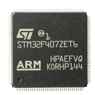
STM32F415ZGT6 - 168MHz ARM Cortex-M4F MCU, 1MB Flash | STMicroelectronics
부품 번호: STM32F415ZGT6 ✓ 활성| 수량 | 단가 | 합계 |
|---|---|---|
| 1 | $12.5 | $12.50 |
| 10 | $11.25 | $112.50 |
| 100 | $10 | $1,000.00 |
| 500 | $9 | $4,500.00 |
| 1,000 | $8.5 | $8,500.00 |
STM32F415ZGT6 개요
What is an ARM Cortex-M4F microcontroller? It is a 32-bit processor core designed for embedded systems that require a balance of performance, power efficiency, and advanced digital signal processing (DSP) capabilities. The 'F' suffix indicates the presence of a hardware floating-point unit, which accelerates mathematical operations for applications like motor control, audio processing, and sensor fusion. In the system hierarchy, a microcontroller (MCU) integrates the processor core, memory, and peripherals on a single chip, serving as the 'brain' of embedded systems. The STM32F4 series sits in the high-performance tier of ST's STM32 portfolio, positioned above the mainstream F1/F3 series and below the higher-end F7/H7 series.
Key features of the STM32F415ZGT6 include a 168 MHz CPU with 210 DMIPS performance, 1 MB of Flash memory, 192 KB of SRAM, and a comprehensive set of peripherals: three 12-bit ADCs (up to 24 channels), two 12-bit DACs, advanced timers, and multiple communication interfaces (USART, SPI, I2C, USB OTG FS/HS, CAN, SDIO, and Ethernet MAC). The device also features a true random number generator (RNG), a cryptographic acceleration cell (AES, DES, 3DES), and a camera interface (DCMI). These features make it ideal for applications requiring high computational throughput and rich connectivity.
From a technical architecture perspective, the STM32F415ZGT6 is built on a 90nm process technology, offering a good balance of performance and power consumption. The Cortex-M4F core includes a single-precision FPU and DSP instructions, enabling efficient execution of complex algorithms. The memory architecture uses a Harvard bus structure with separate instruction and data buses, allowing simultaneous access to Flash and SRAM. The device supports a wide supply voltage range of 1.8V to 3.6V, with a comprehensive clock management system including a PLL, multiple internal/external oscillators, and a real-time clock (RTC).
Typical applications include industrial motor control, medical devices, consumer electronics, IoT gateways, and audio processing. The combination of high-speed ADC, advanced timers, and Ethernet MAC makes it particularly well-suited for real-time control and networked systems. For example, in a motor control application, the advanced PWM timers and high-resolution ADC enable precise current and speed regulation.
When designing with this device, pay attention to power supply decoupling: place a 100nF capacitor close to each VDD pin and a 4.7uF bulk capacitor on the main supply. Also, ensure proper configuration of the boot pins (BOOT0 and BOOT1) to select the desired boot source. The device supports in-circuit programming and debugging via SWD and JTAG interfaces, facilitating development.
드롭인 대체품: STM32F415ZGT6 — 동일 패키지, 핀 호환. PCB 재작업이 필요한 다른 패키지 부품은 제외됩니다.
이 시리즈의 변형
다음과 드롭인 호환되는 동일 시리즈 모델: STM32F415ZGT6 (동일 폼 팩터 및 풋프린트) — 차이점: ADC, Communication Interfaces, Package, Timers, SRAM.
빠른 비교 도구 — 나란히 비교할 대체 부품을 선택하십시오:
STM32F407ZGT6
✅ 드롭인✓ 재고 있음
$5.25 / 개
데이터시트 보기 →STM32F417ZGT6
✅ 드롭인✓ 재고 있음
$8.1 / 개
데이터시트 보기 →STM32F415ZGT7
✅ 드롭인 ⚠️ 사양 미검증📋 참조 대체품 (카탈로그에 없음)
STM32F405ZGT6
✅ 드롭인 ⚠️ 사양 미검증✓ 재고 있음
$8.1 / 개
데이터시트 보기 →STM32F415ZGT6 최대 정격 & 전기적 특성
| Core | ARM Cortex-M4F with FPU |
| 최대 클록 주파수 | 168 MHz |
| Flash Memory | 1 MB |
| SRAM | 192 KB |
| 공급 전압 | 1.8V to 3.6V |
| 패키지 | LQFP144 (20x20 mm) |
| 핀 수 | 144 |
| GPIO Pins | 114 |
| ADC | 3x 12-bit, up to 24 channels |
| DAC | 2x 12-bit |
| Timers | Advanced-control, general-purpose, basic, and low-power timers |
| Communication Interfaces | USART, SPI, I2C, USB OTG FS/HS, CAN, SDIO, Ethernet MAC |
| 동작 온도 | -40C to +85C |
| RoHS 상태 | Compliant |
| DSP Instructions | Yes |
| Floating-Point Unit | Single-precision |
STM32F415ZGT6 핀 구성
| 핀 1 | PE2 — GPIO / alternate functions |
| 핀 2 | PE3 — GPIO / alternate functions |
| 핀 3 | PE4 — GPIO / alternate functions |
| 핀 4 | PE5 — GPIO / alternate functions |
| 핀 5 | PE6 — GPIO / alternate functions |
| 핀 6 | VBAT — Backup battery supply |
| 핀 7 | PC13 — GPIO / RTC tamper |
| 핀 8 | PC14 — GPIO / OSC32_IN |
| 핀 9 | PC15 — GPIO / OSC32_OUT |
| 핀 10 | PF0 — GPIO / OSC_IN |
| 핀 11 | PF1 — GPIO / OSC_OUT |
| 핀 12 | PF2 — GPIO |
| 핀 13 | PF3 — GPIO |
| 핀 14 | PF4 — GPIO |
| 핀 15 | PF5 — GPIO |
| 핀 16 | PF6 — GPIO |
| 핀 17 | PF7 — GPIO |
| 핀 18 | PF8 — GPIO |
| 핀 19 | PF9 — GPIO |
| 핀 20 | PF10 — GPIO |
| 핀 21 | VSS — Ground |
| 핀 22 | VDD — Power supply |
| 핀 23 | PF11 — GPIO |
| 핀 24 | PF12 — GPIO |
| 핀 25 | PF13 — GPIO |
| 핀 26 | PF14 — GPIO |
| 핀 27 | PF15 — GPIO |
| 핀 28 | PG0 — GPIO |
| 핀 29 | PG1 — GPIO |
| 핀 30 | PG2 — GPIO |
| 핀 31 | PG3 — GPIO |
| 핀 32 | PG4 — GPIO |
| 핀 33 | PG5 — GPIO |
| 핀 34 | PG6 — GPIO |
| 핀 35 | PG7 — GPIO |
| 핀 36 | PG8 — GPIO |
| 핀 37 | PG9 — GPIO |
| 핀 38 | PG10 — GPIO |
| 핀 39 | PG11 — GPIO |
| 핀 40 | PG12 — GPIO |
| 핀 41 | PG13 — GPIO |
| 핀 42 | PG14 — GPIO |
| 핀 43 | PG15 — GPIO |
| 핀 44 | VSS — Ground |
| 핀 45 | VDD — Power supply |
| 핀 46 | PD0 — GPIO / crystal oscillator |
| 핀 47 | PD1 — GPIO / crystal oscillator |
| 핀 48 | PD2 — GPIO |
| 핀 49 | PD3 — GPIO |
| 핀 50 | PD4 — GPIO |
| 핀 51 | PD5 — GPIO |
| 핀 52 | PD6 — GPIO |
| 핀 53 | PD7 — GPIO |
| 핀 54 | PD8 — GPIO |
| 핀 55 | PD9 — GPIO |
| 핀 56 | PD10 — GPIO |
| 핀 57 | PD11 — GPIO |
| 핀 58 | PD12 — GPIO |
| 핀 59 | PD13 — GPIO |
| 핀 60 | PD14 — GPIO |
| 핀 61 | PD15 — GPIO |
| 핀 62 | PC0 — GPIO / ADC input |
| 핀 63 | PC1 — GPIO / ADC input |
| 핀 64 | PC2 — GPIO / ADC input |
| 핀 65 | PC3 — GPIO / ADC input |
| 핀 66 | VSSA — Analog ground |
| 핀 67 | VDDA — Analog power supply |
| 핀 68 | PC4 — GPIO / ADC input |
| 핀 69 | PC5 — GPIO / ADC input |
| 핀 70 | PB0 — GPIO / ADC input |
| 핀 71 | PB1 — GPIO / ADC input |
| 핀 72 | PB2 — GPIO |
| 핀 73 | PB3 — GPIO / JTDO |
| 핀 74 | PB4 — GPIO / NJTRST |
| 핀 75 | PB5 — GPIO |
| 핀 76 | PB6 — GPIO / I2C1_SCL |
| 핀 77 | PB7 — GPIO / I2C1_SDA |
| 핀 78 | BOOT0 — Boot mode selection |
| 핀 79 | PB8 — GPIO / I2C1_SCL |
| 핀 80 | PB9 — GPIO / I2C1_SDA |
| 핀 81 | VSS — Ground |
| 핀 82 | VDD — Power supply |
| 핀 83 | PE7 — GPIO |
| 핀 84 | PE8 — GPIO |
| 핀 85 | PE9 — GPIO |
| 핀 86 | PE10 — GPIO |
| 핀 87 | PE11 — GPIO |
| 핀 88 | PE12 — GPIO |
| 핀 89 | PE13 — GPIO |
| 핀 90 | PE14 — GPIO |
| 핀 91 | PE15 — GPIO |
| 핀 92 | PB10 — GPIO / I2C2_SCL |
| 핀 93 | PB11 — GPIO / I2C2_SDA |
| 핀 94 | PB12 — GPIO / SPI2_NSS |
| 핀 95 | PB13 — GPIO / SPI2_SCK |
| 핀 96 | PB14 — GPIO / SPI2_MISO |
| 핀 97 | PB15 — GPIO / SPI2_MOSI |
| 핀 98 | PD8 — GPIO / USART3_TX |
| 핀 99 | PD9 — GPIO / USART3_RX |
| 핀 100 | PD10 — GPIO / USART3_CK |
| 핀 101 | PD11 — GPIO / USART3_CTS |
| 핀 102 | PD12 — GPIO / USART3_RTS |
| 핀 103 | PD13 — GPIO |
| 핀 104 | PD14 — GPIO |
| 핀 105 | PD15 — GPIO |
| 핀 106 | PC6 — GPIO / I2S2_MCK |
| 핀 107 | PC7 — GPIO / I2S2_MCK |
| 핀 108 | PC8 — GPIO / SDIO_D0 |
| 핀 109 | PC9 — GPIO / SDIO_D1 |
| 핀 110 | PA0 — GPIO / ADC input / WKUP |
| 핀 111 | PA1 — GPIO / ADC input |
| 핀 112 | PA2 — GPIO / USART2_TX |
| 핀 113 | PA3 — GPIO / USART2_RX |
| 핀 114 | VSS — Ground |
| 핀 115 | VDD — Power supply |
| 핀 116 | PA4 — GPIO / SPI1_NSS |
| 핀 117 | PA5 — GPIO / SPI1_SCK |
| 핀 118 | PA6 — GPIO / SPI1_MISO |
| 핀 119 | PA7 — GPIO / SPI1_MOSI |
| 핀 120 | PA8 — GPIO / USB_OTG_FS_SOF |
| 핀 121 | PA9 — GPIO / USB_OTG_FS_VBUS |
| 핀 122 | PA10 — GPIO / USB_OTG_FS_ID |
| 핀 123 | PA11 — GPIO / USB_OTG_FS_DM |
| 핀 124 | PA12 — GPIO / USB_OTG_FS_DP |
| 핀 125 | PA13 — GPIO / SWDIO |
| 핀 126 | PA14 — GPIO / SWCLK |
| 핀 127 | PA15 — GPIO / JTDI |
| 핀 128 | PC10 — GPIO / SDIO_D2 |
| 핀 129 | PC11 — GPIO / SDIO_D3 |
| 핀 130 | PC12 — GPIO / SDIO_CK |
| 핀 131 | PD0 — GPIO / crystal oscillator |
| 핀 132 | PD1 — GPIO / crystal oscillator |
| 핀 133 | PD2 — GPIO |
| 핀 134 | PD3 — GPIO |
| 핀 135 | PD4 — GPIO |
| 핀 136 | PD5 — GPIO |
| 핀 137 | PD6 — GPIO |
| 핀 138 | PD7 — GPIO |
| 핀 139 | VSS — Ground |
| 핀 140 | VDD — Power supply |
| 핀 141 | PB0 — GPIO / ADC input |
| 핀 142 | PB1 — GPIO / ADC input |
| 핀 143 | PB2 — GPIO |
| 핀 144 | PB3 — GPIO / JTDO |
일반적인 애플리케이션
STM32F415ZGT6 적합 용도: 6 애플리케이션s: Industrial Motor Control, IoT Gateway, Medical Device, Audio Processing, Smart Home Controller, Test and Measurement.
Industrial Motor Control
The STM32F415ZGT6 is ideal for industrial motor control due to its advanced timers (TIM1/TIM8) that generate complementary PWM with dead-time insertion, and its high-speed 12-bit ADCs that sample phase currents. The FPU accelerates field-oriented control (FOC) algorithms, enabling efficient and precise motor drives. In a typical application, the MCU reads current sensors via the ADC, executes the FOC algorithm in the FPU, and outputs PWM signals to the gate driver. The Ethernet MAC allows remote monitoring and diagnostics. Compared to lower-end MCUs, the 168 MHz clock and DSP instructions reduce control loop latency, improving dynamic response. Designers should ensure proper isolation between power and control stages and use the ADC's injected channels for synchronized sampling.
추천
IoT Gateway
The STM32F415ZGT6 serves as a powerful IoT gateway processor, connecting sensors and devices to the cloud. Its Ethernet MAC and USB OTG interfaces enable wired and wireless connectivity, while multiple UARTs/SPIs/I2Cs interface with various sensors and communication modules (e.g., Wi-Fi, LoRa). The cryptographic acceleration and RNG enhance security for TLS/DTLS protocols. In a typical gateway, the MCU aggregates data from sensors, processes it locally, and transmits it to the cloud via Ethernet or a cellular module. The 1 MB Flash allows storing firmware and buffering data. The FPU accelerates data processing, such as sensor fusion algorithms. Designers should consider power consumption and use low-power modes when idle. The device's industrial temperature range ensures reliable operation in outdoor environments.
추천
Medical Device
The STM32F415ZGT6 is suitable for medical devices such as patient monitors, infusion pumps, and diagnostic equipment. Its high-performance core and FPU enable real-time signal processing for ECG, EEG, and other biosignals. The multiple ADCs and DACs interface with analog front-ends, while the USB OTG supports connectivity to PCs or mobile devices. The cryptographic acceleration ensures secure data transmission, complying with health data privacy regulations. In a typical patient monitor, the MCU samples ECG signals via the ADC, processes them with digital filters, and displays the waveform on an LCD. The device's low power consumption and wide supply voltage range support battery operation. Designers must follow medical safety standards (e.g., IEC 60601) and ensure proper isolation and EMC protection.
추천
Audio Processing
The STM32F415ZGT6 is well-suited for audio processing applications such as audio effects processors, voice recognition, and active noise cancellation. The Cortex-M4F with FPU and DSP instructions efficiently executes audio algorithms like FIR/IIR filters, FFT, and codecs. The I2S interface connects to audio codecs, and the DAC can output analog audio directly. In a typical audio effects processor, the MCU receives digital audio via I2S, applies effects (e.g., reverb, equalization) in real-time, and outputs the processed audio. The 168 MHz clock ensures low latency. The device's large SRAM (192 KB) buffers audio samples. Designers should pay attention to clock jitter and use a dedicated audio PLL for high-quality audio. The low noise ADC and DAC contribute to high signal-to-noise ratio.
추천
Smart Home Controller
The STM32F415ZGT6 acts as a central controller in smart home systems, managing lighting, HVAC, security, and appliances. Its rich connectivity (Ethernet, USB, UART, SPI, I2C) allows integration with various smart home protocols (e.g., Zigbee, Z-Wave, Wi-Fi). The device's low power modes enable energy-efficient operation. In a typical smart home hub, the MCU communicates with sensors and actuators, processes user commands, and provides a web interface via Ethernet. The cryptographic acceleration secures communication with cloud services. The 1 MB Flash stores the hub's firmware and configuration. Designers should implement over-the-air (OTA) updates using the dual-bank Flash feature. The device's industrial temperature range ensures reliable operation in home environments.
추천
Test and Measurement
The STM32F415ZGT6 is used in test and measurement equipment such as oscilloscopes, data loggers, and signal generators. Its high-speed ADCs (up to 2.4 MSPS) and DACs enable precise signal acquisition and generation. The advanced timers provide accurate time base and triggering. In a typical data logger, the MCU samples multiple analog channels, timestamps the data, and stores it on an SD card via SDIO. The USB OTG allows connection to a PC for data analysis. The FPU accelerates signal processing, such as FFT for spectrum analysis. The device's wide supply voltage range and low power consumption support portable instruments. Designers should use external precision references and careful PCB layout to maintain measurement accuracy.
추천
추천 제품 요약
엔지니어링 참조 데이터: STM32F415ZGT6 — 비교, 설계 지침 및 규정 준수 정보.
선택 가이드
대체품과의 비교
| 파라미터 | 이 제품 | STM32F407ZGT6 | STM32F417ZGT6 | STM32F415ZGT7 | STM32F405ZGT6 | LPC4357FET256 |
|---|---|---|---|---|---|---|
| Package | LQFP144 | LQFP144 | LQFP144 | LQFP144 | LQFP144 | BGA256 |
| Brand | STMicroelectronics | STMicroelectronics | STMicroelectronics | STMicroelectronics | STMicroelectronics | NXP Semiconductors |
| Core | ARM Cortex-M4F | ARM Cortex-M4F | ARM Cortex-M4F | ARM Cortex-M4F | ARM Cortex-M4F | ARM Cortex-M4F + M0 |
| Max Clock Frequency | 168 MHz | 168 MHz | 168 MHz | 168 MHz | 168 MHz | 204 MHz |
| Flash Memory | 1 MB | 1 MB | 1 MB | 1 MB | 1 MB | 1 MB |
| SRAM | 192 KB | 192 KB | 192 KB | 192 KB | 192 KB | 136 KB |
| Cryptographic Acceleration | Yes (AES, DES, 3DES) | No | Yes (AES, DES, 3DES) | Yes (AES, DES, 3DES) | No | No |
| Ethernet MAC | Yes | Yes | Yes | Yes | No | Yes |
주요 차별점
- Integrated cryptographic acceleration and RNG (vs STM32F407ZGT6)
- Higher SRAM than some alternatives (vs LPC4357FET256)
- Pin-compatible with F4 family (vs STM32F405ZGT6)
설계 노트
Decouple each VDD pin with a 100nF ceramic capacitor placed as close as possible to the pin. Additionally, place a 4.7uF bulk capacitor on the main supply rail. For VDDA, use a dedicated 1uF capacitor and a ferrite bead to isolate analog noise. Ensure VSSA is connected to a clean ground plane.
For the LQFP144 package, use a 4-layer PCB with a solid ground plane. Route high-speed signals (Ethernet, USB) with controlled impedance (e.g., 90 ohms differential for USB). Keep crystal oscillator traces short and away from high-current switching traces. Place the decoupling capacitors on the bottom side directly under the MCU if possible.
Ensure BOOT0 pin is pulled low for normal boot from Flash. If using SWD debugging, note that PA13 (SWDIO) and PA14 (SWCLK) are shared with GPIO; do not use them as GPIO in production without disabling debug. Also, the VBAT pin must be connected to a battery or tied to VDD to preserve RTC functionality.
규정 준수 정보
RoHS and REACH compliant per STMicroelectronics product page. Not AEC-Q100 qualified; for automotive use, consider STM32F415ZGT7 (extended temp) or other automotive-grade variants.