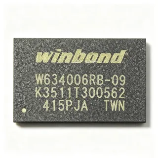
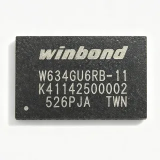
W9751G6NB-25-TR - 512Mb DDR2-800 SDRAM x16 | Winbond
부품 번호: W9751G6NB-25-TR ✓ 활성| 수량 | 단가 | 합계 |
|---|---|---|
| 1 | $0.97 | $0.97 |
| 10 | $0.92 | $9.20 |
| 100 | $0.86 | $86.00 |
| 500 | $0.81 | $405.00 |
| 1,000 | $0.76 | $760.00 |
W9751G6NB-25-TR 개요
DDR2 SDRAM (Double Data Rate 2 Synchronous Dynamic Random Access Memory) is a generation of JEDEC-standard DRAM that transfers data on both clock edges, doubling the effective bandwidth of the predecessor DDR1 while operating from a lower 1.8 V power rail. Within the memory hierarchy, DDR2 SDRAM sits between DDR1 and DDR3 in the dynamic random-access memory (DRAM) family, and remains a cost-effective choice for embedded systems, set-top boxes, and networking equipment whose processors support only DDR2 interfaces.
Key features of the W9751G6NB-25 include the -25 speed grade supporting DDR2-800 operation, a posted CAS with additive latency and auto precharge function, a data mask (DM) function for byte-level write masking, and dynamic on-chip termination (ODT) that improves signal integrity at high data rates by terminating the bus inside the chip. The x16 organization suits systems with narrow 16-bit memory buses or dual-chip 32-bit configurations.
The device uses a standard DDR2 architecture with a 1.8 V nominal supply, differential strobes (DQS, /DQS) for data capture, and burst lengths of 4 or 8 with interleaved or sequential burst ordering. Refresh and self-refresh modes support low-power standby operation between accesses.
Typical applications include set-top boxes, digital TVs, network routers and switches, industrial HMI terminals, and printer or multimedia SoC platforms that specify a 512 Mbit x16 DDR2 memory.
Design-wise, pay attention to DDR2 fly-by clock routing, dynamic ODT settings in the memory controller, and address/command bus termination to meet timing at 400 MHz.
This page synthesizes distributor pricing from LCSC, DigiKey, and Mouser, drop-in family alternatives, and practical design notes not found in the manufacturer datasheet.
드롭인 대체품: W9751G6NB-25-TR — 동일 패키지, 핀 호환. PCB 재작업이 필요한 다른 패키지 부품은 제외됩니다.
이 시리즈의 변형
다음과 드롭인 호환되는 동일 시리즈 모델: W9751G6NB-25-TR (동일 폼 팩터 및 풋프린트) — 차이점: Data Rate, Organization.
빠른 비교 도구 — 나란히 비교할 대체 부품을 선택하십시오:
W9751G6NB-25
✅ 드롭인✓ 재고 있음
$5.6 / 개
데이터시트 보기 →W9751G6NB-3
✅ 드롭인 ⚠️ 사양 미검증📋 참조 대체품 (카탈로그에 없음)
W9751G6NB-25-TR 최대 정격 & 전기적 특성
| 메모리 유형 | SDRAM - DDR2 |
| 메모리 크기 | 512 Mbit |
| 메모리 구성 | 32M x 16 (8M x 4 banks x 16) |
| Number of Banks | 4 |
| Clock Frequency | 400 MHz |
| 데이터 속도 | DDR2-800 (800 MT/s) |
| Access Time | 57.5 ns |
| 인터페이스 | Parallel |
| Supply Voltage (VDD) | 1.8 V (DDR2 standard) |
| 동작 온도 | 0C to +85C |
| Speed Grade | -25 |
| 패키지 | 84-VFBGA (8 x 12.5 mm) |
| 실장 유형 | Surface Mount |
| 특징 | Auto precharge, data mask function, dynamic on-chip termination (ODT) |
| Packaging | Tape & Reel (TR) |
| Refresh | Auto refresh and self-refresh |
| RoHS 상태 | Compliant |
W9751G6NB-25-TR 84-vfbga (8 x 12.5 mm) 핀 구성 가이드
W9751G6NB-25-TR(84-vfbga (8 x 12.5 mm) 패키지)의 핀 구성입니다. 이 디지털 IC에는 GPIO, 통신 인터페이스(UART, SPI, I2C), 전원 핀이 포함되어 있습니다. 대체 핀 기능과 구성 옵션은 제조사 데이터시트를 참조하십시오. 임베디드 시스템 설계와 PCB 레이아웃에 필수적입니다.

다음에 대한 상세 핀아웃 데이터 없음: W9751G6NB-25-TR.
다음을 참조하십시오: 데이터시트 전체 핀 구성은 다음을 참조하십시오.
일반적인 애플리케이션
W9751G6NB-25-TR 적합 용도: 6 애플리케이션s: Set-Top Box and IPTV Platforms, Network Router and Switch Line Cards, Industrial HMI and Touch Panels, Digital TV and Multimedia Processing, Embedded FPGA Processing Systems, Printer and Office Automation Electronics.
Set-Top Box and IPTV Platforms
Set-top box and IPTV SoCs commonly pair a 16-bit DDR2 memory controller with 512 Mbit DRAM for video buffering, channel decoding, and middleware execution. The W9751G6NB-25-TR matches this requirement exactly: its 32M x 16 organization fills a single 16-bit bus, its DDR2-800 (400 MHz clock) rate supplies 1.6 GB/s of peak bandwidth for HD video frame buffers, and dynamic ODT simplifies high-speed bus termination on cost-driven two-layer-class memory topologies. The chip is placed between the SoC memory controller and the 1.8 V rail with fly-by address/command routing; unlike DDR3, no write leveling is required, easing layout and bring-up. Operating from 0C to +85C covers consumer AV cabinet environments.
추천
Network Router and Switch Line Cards
Enterprise and carrier access equipment frequently uses x16 DDR2 DRAM for packet buffers, routing tables, and control-plane software images. The W9751G6NB-25-TR provides 512 Mbit with 57.5 ns random access and DDR2-800 bandwidth, which sustains bursty packet-buffer traffic patterns with auto precharge reducing command overhead on scattered accesses. The data mask function enables efficient partial-packet writes, a common operation in buffer management engines, while self-refresh keeps table data alive through power-state transitions. In a typical design two devices sit side-by-side forming a 32-bit bus at 400 MHz with shared clock fly-by routing; the low 1.8 V interface reduces power versus legacy DDR1 buffers, important for fanless network appliances.
추천
Industrial HMI and Touch Panels
Industrial human-machine interface terminals and touch panels use DDR2 DRAM to hold frame buffers for TFT LCDs and runtime environments such as embedded Linux GUIs. The W9751G6NB-25-TR's x16 organization matches single-bus HMI SoC controllers, and its DDR2-800 rate comfortably supports 1024x768 or WXGA frame refresh with double-buffering. Auto precharge accelerates the scattered row accesses typical of graphical blitting operations. Commercial 0C to +85C operation suits enclosed panel installations, and the 84-ball VFBGA resists shock and vibration better than leaded packages in factory settings. Designers should reserve refresh budget (7.8 us row refresh) in the display pipeline to guarantee deterministic latency on the shared memory bus.
추천
Digital TV and Multimedia Processing
Digital TV main boards and multimedia SoC platforms require DRAM for motion-estimation buffers, de-interlacing, and graphics layers, typically on a 16-bit DDR2 interface. The W9751G6NB-25-TR supplies 1.6 GB/s peak bandwidth at DDR2-800, enough for simultaneous main-picture and PIP frame processing at HD resolutions. Its 4-bank architecture interleaves access between the video decoder and graphics engines, while dynamic on-chip termination maintains signal integrity on dense TV main boards where trace lengths to multiple DRAM loads vary. Designers typically pair it with Winbond SPI NOR for boot code and NAND for content storage, creating a complete Winbond memory ecosystem that simplifies qualification and second sourcing.
추천
Embedded FPGA Processing Systems
FPGA-based embedded systems - image processing, data acquisition, and protocol bridging - often instantiate a DDR2 memory controller IP in the fabric, and many mid-range FPGA families support DDR2 at up to 400 MHz. The W9751G6NB-25-TR is a validated fit: its x16 width suits single-chip controller IPs, its 57.5 ns access time and DDR2-800 timing interface directly with controller calibration engines, and dynamic ODT is supported by common memory-controller calibration schemes. On FPGA boards the VFBGA is placed near the I/O bank with SSTL-18 signaling class drivers. Engineers should run controller calibration at power-up and validate across temperature, since read-data centering shifts with 0C to +85C ambient changes.
추천
Printer and Office Automation Electronics
Laser printers, multifunction devices, and office automation controllers use DDR2 DRAM as page-buffer memory for raster image processing. The W9751G6NB-25-TR offers 512 Mbit - a standard page-buffer size for monochrome print engines - and its 1.6 GB/s DDR2-800 bandwidth keeps the RIP pipeline fed at 30+ pages-per-minute throughput. The data mask function lets the image-processing ASIC patch bitmaps in place without read-modify-write cycles, and auto precharge accelerates the sequential scan pattern of raster memory. The compact 84-VFBGA (8 x 12.5 mm) footprint fits the dense mainboard layouts typical of printers, and consumer-grade temperature range matches office environment specifications.
추천
추천 제품 요약
엔지니어링 참조 데이터: W9751G6NB-25-TR — 비교, 설계 지침 및 규정 준수 정보.
선택 가이드
대체품과의 비교
| 파라미터 | 이 제품 | W9751G6NB-25 | W9751G6NB-3 |
|---|---|---|---|
| Package | 84-VFBGA (8x12.5 mm) | 84-VFBGA (8x12.5 mm) - same | 84-VFBGA (8x12.5 mm) - same |
| Brand | Winbond Electronics | Winbond Electronics | Winbond Electronics |
| Density | 512 Mbit | 512 Mbit | 512 Mbit |
| Organization | 32M x 16 | 32M x 16 | 32M x 16 |
| Data Rate | DDR2-800 (400 MHz) | DDR2-800 (400 MHz) | DDR2-667 (333 MHz) |
| Supply Voltage | 1.8 V (DDR2) | 1.8 V (DDR2) | 1.8 V (DDR2) |
주요 차별점
- Full DDR2-800 speed grade in compact VFBGA (vs W9751G6NB-3)
- Tape-and-reel format for high-volume SMT lines (vs W9751G6NB-25)
- Dynamic on-chip termination reduces BOM (vs Legacy DDR1 SDRAM parts)
설계 노트
At DDR2-800 (400 MHz clock, 800 MT/s), route the address/command/control group in fly-by topology with series termination at the controller and enable dynamic ODT on the DRAM for read/write termination. Length-match DQS/DQS# pairs to their data byte lanes and keep all DDR2 nets referenced to a continuous ground plane. Estimated: with typical FR-4, keep trace skew within the controller's window (commonly +/-25 ps per group) and simulate eye closure before tape-out, since VFBGA escape routing limits tuning space.
The device operates from a 1.8 V VDD/VDDQ rail per the DDR2 standard. Estimated: at DDR2-800 x16 active-read burst, current transients of several hundred milliamps can occur within a clock cycle, so place at least one 0.1 uF ceramic per ball-group cluster plus bulk 10 uF capacitance within 3 mm of the package. Verify the 1.8 V rail droop stays inside tolerance during simultaneous refresh and read bursts; undervoltage during refresh is a common cause of intermittent data errors in the field.
Place the 84-VFBGA within 50 mm of the memory controller to keep flight-time skew manageable at 400 MHz. Fan out BGA balls with via-in-pad or dog-bone escapes on 0.8 mm ball pitch, and dedicate an inner layer as an unbroken DDR2 reference plane. Following the Winbond reference layout in the datasheet design guide simplifies impedance control (50 ohm single-ended, 100 ohm differential DQS). Add test coupons or probe points on DQS and clock for calibration and production debug.
Do not assume DDR1/DDR3 compatibility - the 1.8 V SSTL-18 signaling, ODT register map, and posted-CAS behavior are DDR2-specific, and the x16 ballout differs from x8 parts even in the same ball count. Program EMR2 for the correct dynamic ODT value during initialization, or termination will be absent and signal integrity will fail at DDR2-800. Also respect the 7.8 us average row refresh interval in the controller configuration; extending it to save power without self-refresh mode causes retention errors.
규정 준수 정보
RoHS compliant per distributor listings for this active Winbond part. Commercial temperature grade (0C to +85C); not AEC-Q100 applicable. REACH and halogen-free status not stated in provided data.