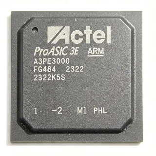
A54SX32A-1FGG484 - 32K Gate FPGA, 484-FBGA | Microchip
MPN: A54SX32A-1FGG484 ✗ End of Life| Qty | Unit Price | Extended |
|---|---|---|
| 1 | $184.61 | $184.61 |
| 10 | $1 | $10.00 |
| 100 | $1 | $100.00 |
| 500 | $1 | $500.00 |
| 1,000 | $1 | $1,000.00 |
A54SX32A-1FGG484 Overview
An FPGA (Field-Programmable Gate Array) is a semiconductor device containing a fabric of programmable logic blocks and interconnects that designers configure after manufacturing. Within the programmable logic hierarchy, the A54SX32A belongs to the one-time-programmable (OTP) antifuse class, positioned under FPGAs, programmable logic ICs, and digital semiconductors. Antifuse technology stores its configuration physically, so it retains programming permanently, powers up instantly, and is inherently resistant to configuration readback.
Key features of the A54SX32A-1FGG484 include 32K gates of SX-A fabric built on a 0.25 micron CMOS process, the -1 standard speed grade, and 249 user-available I/O on the 484-ball fine-pitch BGA. The 2.5 V supply keeps dynamic power low, while the antifuse architecture eliminates configuration PROMs and boot time entirely.
Technically, the SX-A architecture uses a sea-of-modules fabric with combinational and sequential cells connected by antifuse-programmed routing. Because the routing is programmed once, signal paths exhibit low, deterministic impedance, supporting the 278 MHz toggle-rate capability specified for the family. The part is lead free per distributor data (PCB Electronics lists it as LEAD FREE).
Typical applications include glue-logic integration, bus interfacing, industrial control, telecommunications line-card functions, and military/aerospace designs that value the configuration security and instant-on behavior of antifuse FPGAs.
A key design consideration: antifuse devices are one-time programmable, so debugging requires careful up-front simulation; prototype on a slower-speed or larger-density same-family device before committing the -1 speed grade.
This page adds value beyond the datasheet by consolidating distributor pricing, stock levels, drop-in family alternatives, and procurement guidance in one place.
Drop-in alternatives for A54SX32A-1FGG484 — same package, pin-to-pin compatible. Different-package parts requiring PCB rework are excluded.
Variants in this series
Same-series models that are drop-in compatible with A54SX32A-1FGG484 (same form factor and footprint) — differing in Package, Family, Operating Temperature, System Gates, Speed Grade.
Quick Comparison Tool — Select alternative parts for side-by-side comparison:
A54SX32A-1FG484M
✅ Drop-In📋 Reference alternative (not in catalog)
A54SX32A-1FGG484M
✅ Drop-In📋 Reference alternative (not in catalog)
A54SX32A-1FGG484I
✅ Drop-In📋 Reference alternative (not in catalog)
A54SX32A-1FGG484 Maximum Ratings & Electrical Characteristics
| Logic Gates | 32000 gates |
| Usable Cells | 1800 cells |
| User I/O | 249 I/O |
| Maximum System Performance | 278 MHz |
| Process Technology | 0.25 um CMOS |
| Core Supply Voltage | 2.5 V |
| Speed Grade | -1 |
| Programmable Technology | Antifuse (one-time programmable) |
| Family | SX-A (Actel/Microsemi) |
| Package | 484-ball FBGA (FGG484) |
| Mounting Type | Surface Mount |
| Packaging | Tray |
| Lead Free | Yes |
| Configuration Memory | Non-volatile (antifuse, no external config PROM) |
A54SX32A-1FGG484 484-ball fbga (fgg484) Pin Configuration Guide
Pin configuration for A54SX32A-1FGG484 (484-ball fbga (fgg484) package). This digital IC includes GPIO, communication interfaces (UART, SPI, I2C), and power pins. Refer to the manufacturer datasheet for alternate pin functions and configuration options. Essential for embedded system design and PCB layout.

No detailed pinout data available for A54SX32A-1FGG484.
Refer to the datasheet for full pin configuration.
Typical Applications
A54SX32A-1FGG484 is suitable for 6 applications: Glue Logic and System Integration, Industrial Control and Automation, Telecommunications Line Cards, Defense and Aerospace Electronics, Test and Measurement Equipment, Legacy Board Sustainment and Obsolescence Management.
Glue Logic and System Integration
The A54SX32A-1FGG484 excels at consolidating discrete glue logic - bus transceivers, address decoders, state machines, and interrupt controllers - into a single 32K-gate antifuse device. Its 249 user I/O on the 484-ball FBGA provides enough pins to bridge multiple bus widths simultaneously, and the 278 MHz performance rating covers even the fastest legacy processor interfaces. Because the antifuse fabric is programmed once, signal routing impedance is deterministic, simplifying timing closure for decode and interface paths. Replacing dozens of 74-series devices with this one IC reduces board area, BOM line items, and failure points, which is why SX-A parts remain popular in cost-sensitive integration projects maintaining legacy platforms.
Recommended
Industrial Control and Automation
In industrial controllers, PLC I/O cards, and motor-drive interface boards, the A54SX32A-1FGG484 provides 1800 usable cells of deterministic logic operating from a 2.5 V core supply with low dynamic power. The antifuse configuration stores permanently, so the FPGA is functional the instant power is applied - no configuration PROM read time delays the control loop, and a corrupted bitstream cannot occur. The 484-ball FBGA offers abundant I/O (249 pins) for sensor and actuator interfacing. Engineers should budget for one-time-programmability by completing full simulation before programming, since design changes require a new device. Industrial-temperature builds should select the A54SX32A-1FGG484I variant in the same footprint.
Recommended
Telecommunications Line Cards
Telecom line-card designs use the A54SX32A-1FGG484 for backplane interfacing, framing logic, and channel aggregation where 249 user I/O and 278 MHz fabric speed match legacy T1/E1 and backplane signaling requirements. The SX-A family was widely adopted in central-office equipment precisely because its antifuse configuration survives power interruptions without reconfiguration and its routing resistance is fixed at programming time, aiding predictable timing across the fabric. The 2.5 V core reduces power per line card, important in high-density chassis. The 484-ball FBGA provides the pin count needed to connect multiple backplane connectors. For new telecom designs, evaluate Microchip's newer families, but for sustaining existing cards this part remains the direct fit.
Recommended
Defense and Aerospace Electronics
The A54SX32A-1FGG484 suits defense and aerospace subsystems that demand configuration security and instant-on behavior. Antifuse FPGA configuration cannot be read back from the device, protecting proprietary and mission logic from extraction, and the programmed interconnect is inherently immune to configuration-bit upsets that affect SRAM FPGAs in radiation environments. The 32K-gate density with 1800 cells handles protocol bridging, telemetry formatting, and sensor-interface functions, while the 484-ball FBGA supports high-I/O module designs. Designers should verify the required screening and temperature grade (the A54SX32A-1FGG484I industrial variant is DigiKey-stocked) and perform full simulation before programming since antifuse devices are one-time programmable.
Recommended
Test and Measurement Equipment
Bench instruments, fixture controllers, and ATE interface boards leverage the A54SX32A-1FGG484's 278 MHz fabric capability and 249 I/O for pattern generation, capture logic, and instrument bus bridging. The deterministic antifuse routing simplifies the timing analysis needed to guarantee setup and hold at the fixture interface, and the -1 speed grade covers the common timing budgets of parallel test channels. Because the design is programmed once and never reconfigured, measurement repeatability between power cycles is excellent - there is no configuration-load variability. The 484-ball FBGA footprint gives layout flexibility for probing points. Prototype logic on a larger or slower SX-A device before committing, as antifuse parts cannot be reprogrammed.
Recommended
Legacy Board Sustainment and Obsolescence Management
A primary ongoing use of the A54SX32A-1FGG484 is sustaining long-lived platforms - medical devices, avionics, and industrial systems - originally designed around Actel SX-A FPGAs. Because Microchip continues to supply the mature SX-A family, engineers can rebuy the identical 32K-gate, 484-ball FBGA part rather than redesigning. Drop-in variants (A54SX32A-1FG484M, A54SX32A-1FGG484M, A54SX32A-1FGG484I) share the same footprint, letting procurement qualify alternates without PCB change. Stock reported at LCSC and Micro-Semiconductor.com (386 pieces, 2026-09-03) supports bridge buys; the recommended strategy is a lifetime buy sized from failure-rate data, stored per JEDEC moisture-sensitivity handling for FBGA packages.
Recommended
Recommended Products Summary
Engineering reference data for A54SX32A-1FGG484 — comparison, design guidance, and compliance information.
Selection Guide
Comparison with Alternatives
| Parameter | This Product | A54SX32A-1FG484M | A54SX32A-1FGG484M | A54SX32A-1FGG484I |
|---|---|---|---|---|
| Package | 484-ball FBGA (FGG484) | 484-ball FBGA (FG484) - same footprint | 484-ball FBGA (FGG) - same footprint | 484-BGA - same footprint |
| Brand | Microsemi (Microchip Technology) | Microsemi (Microchip Technology) | Microsemi (Microchip Technology) | Microsemi (Microchip Technology) |
| Logic Gates | 32K gates | 32K gates | 32K gates | 32K gates |
| User I/O | 249 | 249 | 249 | 249 |
| Maximum Performance | 278 MHz | 278 MHz | 278 MHz | 278 MHz |
| Core Supply Voltage | 2.5 V | 2.5 V | 2.5 V | 2.5 V |
| Speed Grade | -1 | -1 | -1 | -1 |
Key Differentiators
- Lead-free FGG package flow (vs A54SX32A-1FG484M)
- Industrial temperature availability (vs A54SX32A-1FGG484I)
- Mature antifuse fabric with instant-on security (vs AX250-1FGG484)
Design Notes
The A54SX32A is an antifuse, one-time-programmable FPGA - a programming error or post-tapeout logic change requires a new device. Complete exhaustive simulation (functional and timing) before programming production units, and prototype using a lower-speed or larger SX-A device. Ordering the correct suffix matters: the GG in FGG484 denotes the lead-free package flow versus FG; verify against the Microchip ordering nomenclature in the SX-A datasheet before releasing the BOM.
The SX-A family operates from a single 2.5 V core supply (I/O supplies per datasheet bank definitions), which keeps dynamic power low for a 32K-gate design. Estimated guidance: decouple each supply ball group with at least 0.1 uF ceramic capacitors placed within 2 mm of the package, plus bulk 10 uF per rail. Because antifuse fabric needs no configuration current at power-up, inrush is limited to static ICC only - simplifying power-supply sequencing versus SRAM FPGAs that draw configuration surge current.
The 484-ball FBGA is a fine-pitch BGA requiring controlled-impedance breakout; follow the Microchip SX-A datasheet package chapter for land-pattern and via-in-pad guidance. JEDEC moisture-sensitivity handling applies - bake per MSL rating if the tray seal is broken. Allocate the 249 user I/O across banks according to I/O standard voltage requirements in the datasheet before routing, and reserve ground/power ball groups for clean return paths at the 278 MHz-class edge rates.
Compliance Information
PCB Electronics Supply Chain explicitly lists A54SX32A-1FGG484 as LEAD FREE. The FGG suffix denotes Microsemi's lead-free package flow. Formal RoHS/REACH declarations not found in provided data - verify on Microchip compliance page.