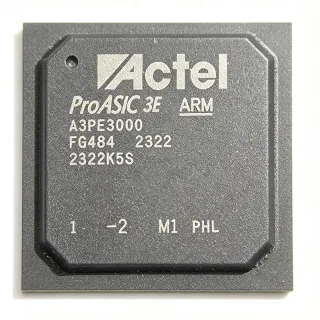
M1AFS1500-2FGG484 - 1.5M Gate Fusion FPGA, 484-BGA | Microchip
MPN: M1AFS1500-2FGG484 ✓ Active| Qty | Unit Price | Extended |
|---|---|---|
| 1 | $251.39 | $251.39 |
| 10 | $238.82 | $2,388.20 |
| 100 | $226.25 | $22,625.00 |
| 500 | $213.68 | $106,840.00 |
| 1,000 | $201.11 | $201,110.00 |
M1AFS1500-2FGG484 Overview
A field-programmable gate array (FPGA) is a semiconductor device containing programmable logic blocks and interconnects that designers configure after manufacturing. Within the programmable logic hierarchy, the M1AFS1500 belongs to the Fusion family of mixed-signal FPGAs, positioned above flash-based ProASIC3-class devices by adding analog peripherals (ADC, analog quad), large flash memory blocks, and comprehensive on-chip clock generation - effectively combining digital programmable logic, analog measurement, and system configuration storage in one chip.
Key features include flash-based configuration (instant-on, non-volatile, SEU-resistant), an embedded ARM Cortex-M1 soft processor option, 4,608-bit dual-port SRAM/FIFO blocks, and integrated CCC/PLL clock conditioning circuits. The -2 speed grade provides higher timing performance than -1 and -0 grades. The 484-ball FBGA with 1.00 mm ball pitch supports high-I/O-count designs in space-constrained boards.
Architecturally, VersaTiles form the logic fabric, each configurable as combinational logic, sequential logic, or memory. The analog quad with ADC enables power-supply and temperature monitoring without external sensors. Flash memory blocks can store firmware for the Cortex-M1 soft core, enabling single-chip embedded systems.
Typical applications include industrial automation and motor control, medical instrumentation, avionics and defense systems requiring non-volatile secure configuration, and test/measurement equipment where mixed-signal integration reduces BOM count.
A key design consideration: power the 1.5V core rail in proper sequence with I/O banks, and plan flash programming access (JTAG/SPI) early in the PCB layout.
This page synthesizes distributor pricing, pin-compatible drop-in alternatives across speed and temperature grades, and practical design notes not found in the manufacturer datasheet. Pricing as of 2026-09-02.
Drop-in alternatives for M1AFS1500-2FGG484 — same package, pin-to-pin compatible. Different-package parts requiring PCB rework are excluded.
Variants in this series
Same-series models that are drop-in compatible with M1AFS1500-2FGG484 (same form factor and footprint) — differing in Package, Process Technology, Family, System Gates, Clock Management.
Quick Comparison Tool — Select alternative parts for side-by-side comparison:
M1AFS1500-2FGG484I
✅ Drop-In✓ In Stock
$201.11 / Unit
View Datasheet →M1AFS1500-1FGG484
✅ Drop-In✓ In Stock
Contact for price
View Datasheet →M1AFS1500-FGG484I
✅ Drop-In✓ In Stock
$152.28 / Unit
View Datasheet →M1AFS1500-2FG484I
✅ Drop-In✓ In Stock
$132 / Unit
View Datasheet →AFS1500-1FGG484I
✅ Drop-In📋 Reference alternative (not in catalog)
M1AFS1500-2FGG484 Maximum Ratings & Electrical Characteristics
| Family | Fusion (M1AFS) Mixed-Signal Flash FPGA |
| System Gates | 1,500,000 |
| Logic Cells | 38,400 |
| User I/O | 223 |
| Flash Memory | 276,480 bits |
| Speed Grade | -2 |
| Maximum Clock Frequency | 350 MHz |
| Core Supply Voltage | 1.5 V |
| Process Technology | 130 nm CMOS |
| Configuration Type | Flash (non-volatile, instant-on) |
| Embedded Processor Option | ARM Cortex-M1 soft core |
| Package | 484-ball FBGA (FGG484) |
| Ball Pitch | 1.00 mm |
| Mounting Type | Surface Mount |
| Packaging | Tray |
| Analog Blocks | ADC / Analog Quad (integrated) |
| RAM Blocks | 4,608-bit dual-port SRAM / FIFO blocks |
M1AFS1500-2FGG484 484-ball fbga (fgg484) Pin Configuration Guide
Pin configuration for M1AFS1500-2FGG484 (484-ball fbga (fgg484) package). This digital IC includes GPIO, communication interfaces (UART, SPI, I2C), and power pins. Refer to the manufacturer datasheet for alternate pin functions and configuration options. Essential for embedded system design and PCB layout.

No detailed pinout data available for M1AFS1500-2FGG484.
Refer to the datasheet for full pin configuration.
Typical Applications
M1AFS1500-2FGG484 is suitable for 6 applications: Industrial Automation and Motor Control, Avionics and Defense Systems, Medical Instrumentation, Test and Measurement Equipment, Secure Embedded Control, Mixed-Signal System Integration.
Industrial Automation and Motor Control
The M1AFS1500-2FGG484 fits industrial automation because its 223 user I/Os interface encoders, sensors, and motor driver stages, while the integrated analog quad with ADC monitors supply rails and die temperature without external supervisory ICs. Flash-based configuration gives instant-on deterministic boot at power-up, essential for factory equipment that must be productive immediately after energization. The ARM Cortex-M1 soft core executes control firmware from the 276,480-bit flash blocks, consolidating sequencing and communication tasks on the same die as the programmable logic. CCC/PLL circuitry synthesizes clean clocks for deterministic PWM timing, and the -2 speed grade provides timing margin for fast control loops running well below the 350 MHz ceiling.
Recommended
Avionics and Defense Systems
Flash-based non-volatile configuration makes the M1AFS1500-2FGG484 attractive for avionics and defense subsystems: there is no external configuration bitstream to intercept or corrupt, and the fabric is inherently resistant to configuration single-event upsets compared with SRAM FPGAs. The 1.5V core at 130 nm keeps power manageable in conduction-cooled enclosures, and the 484-ball FBGA offers 223 I/Os for high-channel-count interface cards. The on-chip ADC supports in-system health monitoring of rails and temperature, a common requirement in flight hardware. Designers can implement redundancy, voting, and built-in-test logic in the 38,400 VersaTile logic cells while the Cortex-M1 handles higher-level diagnostics.
Recommended
Medical Instrumentation
Medical diagnostic instruments benefit from the M1AFS1500-2FGG484's single-chip integration of analog measurement and digital processing. The analog quad ADC digitizes board-level telemetry (supply voltage, die temperature), while the 38,400 logic cells implement acquisition sequencing, filtering, and interface protocols for sensor front ends. Flash configuration ensures the instrument is operational the moment it is switched on - important in clinical settings - and 223 I/Os support multi-channel detector arrays. Because configuration and Cortex-M1 firmware both live in on-chip flash blocks, no external boot device is needed, simplifying regulatory design reviews around firmware integrity and reducing component count on the analog-to-digital acquisition board.
Recommended
Test and Measurement Equipment
In bench instruments and automated test equipment, the M1AFS1500-2FGG484 serves as a flexible timing, protocol, and interconnect engine. The -2 speed grade supports timing paths up to the 350 MHz family maximum, enabling high-resolution event counting and stimulus generation, while 4,608-bit dual-port SRAM/FIFO blocks buffer capture data between clock domains. Its 223 I/Os implement multi-pin bed-of-nails or pod interfaces, and CCC/PLL blocks regenerate clean clocks from noisy references. The integrated ADC lets the instrument log its own rail and thermal conditions for calibration drift analysis. Flash configuration with instant-on boot means the instrument is ready as soon as power is applied, with no configuration latency.
Recommended
Secure Embedded Control
Secure control nodes use the M1AFS1500-2FGG484 because its configuration resides entirely in on-chip flash: there is no external SPI PROM whose bitstream can be snooped during power-up, and no readback window typical of SRAM FPGAs. The ARM Cortex-M1 soft core runs application firmware from the 276,480-bit flash blocks, creating a self-contained processor-plus-logic platform in the 484-ball FBGA. The analog quad monitors supply integrity to detect tamper or fault conditions, and the 223 I/Os drive actuators and secure communication PHYs. Flash configuration is also resistant to radiation-induced upset, extending suitability to infrastructure and critical-control deployments where configuration corruption is unacceptable.
Recommended
Mixed-Signal System Integration
For board designs consolidating discrete ADCs, supervisors, clock generators, and configuration memories into one device, the M1AFS1500-2FGG484 replaces an entire cluster of supporting ICs. Its analog quad with ADC performs power and temperature telemetry; CCC/PLL circuitry replaces a standalone clock conditioner; flash blocks replace the configuration PROM and firmware EEPROM; and 38,400 logic cells implement glue logic that previously occupied multiple CPLDs. The 1.5V core and 130 nm process keep total power below multi-chip equivalents, and the 1.00 mm ball pitch 484-FBGA fits standard BGA assembly flows. Consolidation reduces BOM count, assembly cost, and failure points in compact embedded systems.
Recommended
Recommended Products Summary
Engineering reference data for M1AFS1500-2FGG484 — comparison, design guidance, and compliance information.
Selection Guide
Comparison with Alternatives
| Parameter | This Product | M1AFS1500-2FGG484I | M1AFS1500-1FGG484 | M1AFS1500-FGG484I | M1AFS1500-2FG484I | AFS1500-1FGG484I |
|---|---|---|---|---|---|---|
| Package | 484-ball FBGA (FGG484) | 484-ball FBGA (FGG484) - same | 484-ball FBGA (FGG484) - same | 484-ball FBGA (FGG484) - same | 484-ball FBGA (FG484) - same footprint | 484-ball FBGA (FGG484) - same |
| Brand | Microchip Technology | Microchip Technology | Microchip Technology | Microchip Technology | Microchip Technology | Microchip Technology (Microsemi legacy code) |
| System Gates | 1,500,000 | 1,500,000 | 1,500,000 | 1,500,000 | 1,500,000 | 1,500,000 |
| User I/O | 223 | 223 | 223 | 223 | 223 | 223 |
| Speed Grade | -2 | -2 | -1 | standard | -2 | -1 |
| Temperature Grade | Commercial | Industrial (I) | Commercial | Industrial (I) | Industrial (I) | Industrial (I) |
| Configuration | Flash, non-volatile (276,480 bits) | Flash, non-volatile - same | Flash, non-volatile - same | Flash, non-volatile - same | Flash, non-volatile - same | Flash, non-volatile - same |
Key Differentiators
- Fastest family speed grade (-2) (vs M1AFS1500-1FGG484)
- Industrial temperature drop-in available (vs M1AFS1500-2FGG484I)
- Integrated analog quad with ADC (vs AFS1500-1FGG484I)
Design Notes
Power the 1.5V core and I/O bank rails in the sequence specified in the Fusion family datasheet to guarantee clean flash configuration and avoid latch-up. Provide local bulk capacitance plus 0.1 uF ceramic decoupling at each supply group of the 484-ball FBGA, placed on the opposite PCB side directly under the package. Estimated: with typical Fusion core currents of several hundred milliamps at 1.5V, budget the core regulator at 1 A or more with headroom for worst-case activity. Use the on-chip analog quad ADC to monitor rails and die temperature in-system.
The 484-ball FBGA with 1.00 mm pitch requires a controlled-expansion PCB stack; escape routing typically uses via-in-pad or dog-bone fanout on 0.8-1.0 mm pitch patterns. Define the land pattern per the manufacturer datasheet package addendum and reserve JTAG/FlashPro programming access points early - retrofitting programming headers is a common pitfall on dense FPGA boards. Keep analog quad inputs routed away from high-slew I/O to preserve ADC accuracy. A minimum 4-layer stack with dedicated ground plane is recommended for signal integrity across 223 I/Os.
Do not interchange speed grades without re-running timing closure in Libero SoC: M1AFS1500-1FGG484 (-1) is pin compatible with the -2 part but may fail timing in designs near the 350 MHz limit. Confirm the ordering-code suffix (FG vs FGG ball finish, I temperature grade) when substituting, since legacy Microsemi AFS1500 codes and Microchip M1AFS1500 codes denote the same silicon but different plating/temperature options. Finally, remember flash configuration is instant-on - ensure external circuitry tolerates immediate I/O activity at power application.
Compliance Information
The FGG suffix denotes the lead-free, RoHS-oriented ball finish variant per Microchip ordering-code conventions. REACH and halogen-free status not stated in provided data - verify on the Microchip product page.