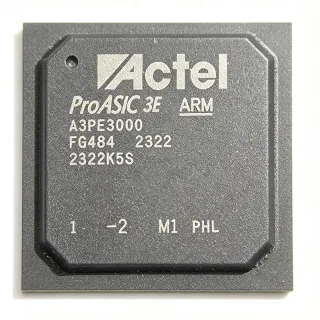
A54SX72A-1FGG484I - 108K-Gate Antifuse FPGA 484-BGA | Microchip
MPN: A54SX72A-1FGG484I ✓ Active| Qty | Unit Price | Extended |
|---|---|---|
| 1 | $320 | $320.00 |
| 10 | $295 | $2,950.00 |
| 100 | $268 | $26,800.00 |
| 500 | $245 | $122,500.00 |
| 1,000 | $225 | $225,000.00 |
A54SX72A-1FGG484I Overview
An antifuse FPGA is a field-programmable gate array whose interconnect switches are permanently programmed at power-up programming time, unlike SRAM-based FPGAs that reload configuration from external memory on every power cycle. Within the programmable logic hierarchy, the SX-A sits in the one-time-programmable (OTP) FPGA category, providing non-volatile configuration without a configuration PROM, which improves design security and reduces board-level component count.
Key features include 108K usable system gates, deterministic sub-nanoseand-class antifuse interconnect delays that do not vary with routing congestion, quadrant and global clocking resources (CLKA, CLKB, and QCLK networks), and a low-power 2.5V core. The 484-ball FGG484 package maximizes I/O availability at 360 user pins, supporting wide bus interfaces and parallel data paths in a single chip.
The SX-A architecture is built from Combinatorial Modules and Register Modules organized in clusters, delivering fast, predictable carry logic for arithmetic functions. Because configuration is stored in antifuse elements, the bitstream is not externally readable, giving inherent resistance to design cloning compared with SRAM FPGAs.
Typical applications include industrial control and automation, communications and networking line cards, military and aerospace boards requiring one-time-programmable security, medical equipment, and glue-logic integration that replaces multiple ASIC/SSI devices for cost savings.
When designing with the A54SX72A, plan the design flow in Libero SoC (or legacy Actel Designer) and verify I/O bank voltage compatibility, since the -1 speed grade and industrial temperature suffix define timing and environmental limits that cannot be changed after programming.
This page adds value beyond the manufacturer datasheet by consolidating distributor availability, drop-in family alternates, comparison tables, and practical design notes in one place.
Drop-in alternatives for A54SX72A-1FGG484I — same package, pin-to-pin compatible. Different-package parts requiring PCB rework are excluded.
Variants in this series
Same-series models that are drop-in compatible with A54SX72A-1FGG484I (same form factor and footprint) — differing in Package, RoHS Status, Operating Temperature, System Gates, Speed Grade.
Quick Comparison Tool — Select alternative parts for side-by-side comparison:
A54SX72A-1FGG484A
✅ Drop-In📋 Reference alternative (not in catalog)
A54SX72A-1FG484I
✅ Drop-In✓ In Stock
$208.5 / Unit
View Datasheet →A54SX72A-2FGG484I
✅ Drop-In✓ In Stock
$112 / Unit
View Datasheet →A54SX72A-FGG484
✅ Drop-In✓ In Stock
$118.6 / Unit
View Datasheet →A54SX72A-1FGG484
✅ Drop-In✓ In Stock
$515 / Unit
View Datasheet →A54SX72A-1FGG484I Maximum Ratings & Electrical Characteristics
| Family | SX-A (Antifuse FPGA) |
| System Gates | 108000 gates |
| Typical Gates | 72000 gates |
| Logic Cells / Modules | 4024 cells |
| Configurable Logic Blocks (CLBs) | 6036 |
| User I/O | 360 |
| Maximum System Frequency | 250 MHz |
| Process Technology | 0.25 um CMOS |
| Core Supply Voltage | 2.5 V |
| Speed Grade | -1 |
| Program Type | One-Time Programmable (Antifuse) |
| Package | 484-ball FBGA (FGG484) |
| Mounting Type | Surface Mount |
| RoHS Status | Lead Free (per distributor listing) |
| Configuration Memory | Non-volatile antifuse (no external configuration PROM required) |
A54SX72A-1FGG484I 484-ball fbga (fgg484) Pin Configuration Guide
Pin configuration for A54SX72A-1FGG484I (484-ball fbga (fgg484) package). This digital IC includes GPIO, communication interfaces (UART, SPI, I2C), and power pins. Refer to the manufacturer datasheet for alternate pin functions and configuration options. Essential for embedded system design and PCB layout.

No detailed pinout data available for A54SX72A-1FGG484I.
Refer to the datasheet for full pin configuration.
Typical Applications
A54SX72A-1FGG484I is suitable for 6 applications: Industrial Control and Automation, Communications and Networking Line Cards, Military and Aerospace Secure Logic, Medical Equipment, ASIC Prototyping and Glue-Logic Integration, 5G Infrastructure and Test Equipment.
Industrial Control and Automation
The A54SX72A-1FGG484I suits industrial controllers because its 108K system gates and 360 user I/O let designers integrate PLC glue logic, bus interfaces, and sequencing functions that previously required several ASICs or SSI devices, cutting board cost. The industrial temperature suffix ensures operation on factory floors, and the antifuse configuration powers up instantly with no configuration load time - important for machinery requiring deterministic startup. Its 2.5V core keeps power modest, while 250 MHz capability covers timing-critical encoder and motion-control paths. Trade-off: the design cannot be field-updated, so logic must be frozen at production.
Recommended
Communications and Networking Line Cards
In networking and communications equipment, the A54SX72A-1FGG484I provides deterministic, sub-nanoseand-class antifuse routing delays that simplify timing closure for backplane interfaces, framer glue logic, and control-plane bridges. The 360 user I/O of the FGG484 package supports wide parallel data buses to PHY and MAC devices, and the quadrant clocking (CLKA, CLKB, QCLK) resources per the SX-A datasheet distribute clocks across card regions with low skew. Because configuration is non-volatile, line cards meet carrier uptime expectations without configuration boot delays. Designers should budget I/O bank voltages carefully in Libero SoC.
Recommended
Military and Aerospace Secure Logic
Antifuse FPGAs are a classic choice for defense and aerospace boards because the programmed bitstream is physically burned into the device and cannot be read back, providing inherent design security that SRAM FPGAs lack. The A54SX72A shares its die architecture with the radiation-tolerant RT54SX72S, giving a documented migration path per Microchip application notes. With 108K gates and one-time programming, single-chip integration replaces multiple sensitive devices, shrinking board area and supply chain exposure. The industrial -I grade version fits ruggedized ground systems; space programs should evaluate the RT variant instead.
Recommended
Medical Equipment
Distributor listings tag the A54SX72A-1FGG484I for medical equipment, where its instant-on antifuse configuration supports diagnostic instruments that must be ready immediately at power-up. The 108K-gate density integrates sensor interface sequencing, display control, and interface bridging in one chip, and the 360 I/O handles multi-channel analog front-end control from ADS1220-class precision ADCs. Non-volatile configuration eliminates the boot-flash failure point, improving instrument reliability ratings. Because logic is fixed after programming, regulated medical designs benefit from a stable, auditable hardware configuration across production units and service replacements.
Recommended
ASIC Prototyping and Glue-Logic Integration
The SX-A family was designed to integrate multiple functions into a low-cost single-chip solution, per Microchip's product positioning, making the A54SX72A-1FGG484I effective for ASIC prototyping, bus-bridge glue logic, and obsolescence-driven redesign. Deterministic antifuse routing means prototype timing closely tracks production timing, and the 0.25 um CMOS process offers mature, stable characteristics. The 484-ball package gives abundant I/O for emulating wide ASIC buses. The limitation is one-time programmability: each design iteration requires a new device, so teams should validate thoroughly in simulation before programming hardware.
Recommended
5G Infrastructure and Test Equipment
Distribution channels associate this part with 5G technology applications, where it serves as control-plane fabric, framer interface, and test-instrument measurement logic. The 250 MHz system speed and quadrant clock networks handle timing distribution across radio-unit control boards, while 108K gates accommodate protocol glue and buffer management. Antifuse security protects proprietary radio algorithms from cloning, an advantage over SRAM FPGAs in the field. For 5G test equipment, the fixed configuration guarantees repeatable instrument behavior between calibrations. Engineers should verify the industrial temperature rating against outdoor-unit (ODU) environmental requirements before selection.
Recommended
Recommended Products Summary
Engineering reference data for A54SX72A-1FGG484I — comparison, design guidance, and compliance information.
Selection Guide
Comparison with Alternatives
| Parameter | This Product | A54SX72A-1FGG484A | A54SX72A-1FG484I | A54SX72A-2FGG484I | A54SX72A-FGG484 |
|---|---|---|---|---|---|
| Package | 484-ball FBGA (FGG484) | 484-ball FBGA (FGG484) - same | 484-ball FBGA (FG484) - same footprint, standard finish | 484-ball FBGA (FGG484) - same | 484-ball FBGA (FGG484) - same |
| Brand | Microchip Technology (Actel/Microsemi) | Microchip Technology | Microchip Technology | Microchip Technology | Microchip Technology |
| System Gates | 108K (72K typical) | 108K | 108K | 108K | 108K |
| User I/O | 360 | 360 | 360 | 360 | 360 |
| Core Supply Voltage | 2.5 V | 2.5 V | 2.5 V | 2.5 V | 2.5 V |
| Programming Type | Antifuse (OTP) | Antifuse (OTP) | Antifuse (OTP) | Antifuse (OTP) | Antifuse (OTP) |
Key Differentiators
- Higher speed grade available as drop-in upgrade (vs A54SX72A-2FGG484I)
- Industrial temperature qualification (vs A54SX72A-1FGG484A)
- Lead-free ball metallurgy for RoHS assembly (vs A54SX72A-1FG484I)
- Non-volatile secure configuration (vs SRAM FPGAs (e.g., M7A3PE1500-FG484 class parts))
Design Notes
The SX-A family operates from a 2.5V core supply on the A54SX72A die. Power rails should be sequenced and decoupled per the Microchip SX-A datasheet power guidelines; place bulk and 0.1uF ceramic decoupling at the FGG484 power ball clusters. Because antifuse FPGAs draw no configuration current at power-up, inrush is governed mainly by I/O bank charging - size the 2.5V regulator for steady-state logic activity plus I/O switching, not configuration surge as with SRAM FPGAs.
The A54SX72A is one-time programmable: an error in the programmed design cannot be corrected on the same device. Always complete post-layout timing simulation and verify pin assignments in Libero SoC (or legacy Actel Designer) before programming production units. Clock planning must respect the quadrant architecture - per the datasheet, refer to the 'Global Clock Networks in Actel's Antifuse Devices' and 'Using A54SX72A and RT54SX72S Quadrant Clocks' application notes for CLKA, CLKB, and QCLK usage before committing routing.
The FGG484 is a 484-ball BGA requiring controlled reflow profiles and X-ray inspection capability; verify pad geometry against the datasheet FGG484 mechanical drawing and follow IPC-recommended BGA land patterns. Fan out power and ground balls with via-in-pad or dogbone escapes on at least a 6-layer board with dedicated power/ground planes to support the 360 user I/O signal integrity. Confirm the FGG (lead-free) versus FG (standard finish) reflow temperature profile matches your assembly process.
With up to 360 switching I/O in one package, simultaneous switching noise is the dominant signal-integrity risk. Group high-toggle-rate buses toward I/O banks with adjacent ground returns, use the datasheet-specified I/O standards and drive strengths in Libero SoC, and add series termination on fast single-ended lines. Measure SSO margins on prototype boards before committing the one-time-programmed production design, since adjustments after programming require new devices.
Compliance Information
Distributor listings identify A54SX72A-1FGG484I as LEAD FREE (PCB Electronics listing). FGG suffix denotes lead-free package finish. REACH, halogen-free, and conflict-minerals status not stated in provided data.