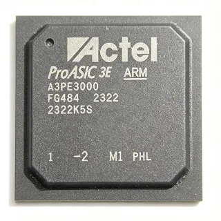
A3P600-1FGG484 - 600K Gate ProASIC3 FPGA, 235 I/O | Microchip
MPN: A3P600-1FGG484 ✓ Active| Qty | Unit Price | Extended |
|---|---|---|
| 1 | $78.5 | $78.50 |
| 10 | $71.2 | $712.00 |
| 100 | $64.9 | $6,490.00 |
| 500 | $58.75 | $29,375.00 |
| 1,000 | $52.4 | $52,400.00 |
A3P600-1FGG484 Overview
A flash-based FPGA is a field-programmable gate array whose configuration is stored in on-chip flash memory cells rather than in an external configuration device or volatile SRAM. In the programmable logic hierarchy, FPGAs sit above CPLDs and below full ASIC custom silicon, occupying the role of reprogrammable system logic. Because ProASIC3 devices are nonvolatile, they power up instantly without a boot sequence and eliminate the BOM cost of a serial configuration flash.
Key features include 600,000 system gates implemented with VersaTiles, four I/O banks with independent VCCIB supply rails, embedded memory of 110592 bits, and support for popular single-ended and differential I/O standards. The -1 speed grade balances performance and power for cost-sensitive systems, while 484 solder balls provide high I/O density and reliable power/signal distribution.
Architecturally, the ProASIC3 fabric consists of a sea-of-VersaTiles over a segmented routing mesh, with embedded SRAM blocks distributed across the die. The 130nm flash process stores configuration as transistor threshold voltages, making the device immune to configuration upset and reducing radiation sensitivity relative to SRAM FPGAs. Design entry uses Libero SoC (Synplify synthesis, ModelSim simulation).
Typical applications include industrial automation controllers, aerospace/defense glue logic and reconfigurable coprocessing, medical instrument interfaces, and communications bridge logic where instant-on, single-chip, high-I/O programmable logic is required.
A key design consideration is power supply partitioning: assign only electrically compatible I/O standards to the same VCCIB bank, since the 484-ball package routes each bank's supply independently.
This page synthesizes distributor pricing, verified drop-in family alternatives, and practical design notes not consolidated in the manufacturer datasheet.
Drop-in alternatives for A3P600-1FGG484 — same package, pin-to-pin compatible. Different-package parts requiring PCB rework are excluded.
Variants in this series
Same-series models that are drop-in compatible with A3P600-1FGG484 (same form factor and footprint) — differing in Package, Configuration Memory, RoHS Status, Family, Core Supply Voltage.
Quick Comparison Tool — Select alternative parts for side-by-side comparison:
A3P600L-FG484
✅ Drop-In✓ In Stock
$85.9 / Unit
View Datasheet →A3P600L-FGG484I
✅ Drop-In✓ In Stock
$41.35 / Unit
View Datasheet →A3P600L-1FGG484I
✅ Drop-In✓ In Stock
$17.1 / Unit
View Datasheet →A3P600-1FGG484I
✅ Drop-In ⚠️ Specs Unverified✓ In Stock
$79.6 / Unit
View Datasheet →A3PE600-1FGG484
✅ Drop-In✓ In Stock
$44.9 / Unit
View Datasheet →A3P600-1FGG484 Maximum Ratings & Electrical Characteristics
| Family | ProASIC3 |
| System Gates | 600,000 |
| Logic Elements / VersaTiles | 13824 |
| User I/O | 235 |
| Embedded Memory | 110592 |
| Maximum System Frequency | 272 MHz |
| Core Voltage | 1.5 V |
| Process Technology | 130 nm CMOS flash |
| Speed Grade | -1 |
| Configuration Memory | Nonvolatile flash (single chip) |
| I/O Banks | 4 |
| Package | 484-ball FBGA (FGG484) |
| Mounting Type | Surface Mount |
| RoHS Status | Compliant |
| Design Software | Microchip Libero SoC |
| Packaging | Tray |
A3P600-1FGG484 484-ball fbga (fgg484) Pin Configuration Guide
Pin configuration for A3P600-1FGG484 (484-ball fbga (fgg484) package). This digital IC includes GPIO, communication interfaces (UART, SPI, I2C), and power pins. Refer to the manufacturer datasheet for alternate pin functions and configuration options. Essential for embedded system design and PCB layout.

No detailed pinout data available for A3P600-1FGG484.
Refer to the datasheet for full pin configuration.
Typical Applications
A3P600-1FGG484 is suitable for 6 applications: Industrial Automation Controllers, Aerospace and Defense Reconfigurable Logic, Medical Instrument Interface Logic, Communications Bridge Logic, Test and Measurement Equipment, Embedded System Glue Logic and I/O Expansion.
Industrial Automation Controllers
The A3P600-1FGG484's 235 user I/Os and four independently powered I/O banks make it a strong fit for industrial automation controllers that must bridge many sensor, encoder, and actuator interfaces. Because its flash fabric is nonvolatile, the controller logic is active within microseconds of power-up with no configuration device to fail in electrically noisy factory environments. Typical use places the FPGA between a 24V industrial backplane translator layer and an MCU or CPU, with VCCIB banks set to 3.3V, 2.5V, or 1.8V as required per standard. The 600K-gate capacity handles multiple protocol cores such as UART/SPI bridges and simple motion sequencing simultaneously.
Recommended
Aerospace and Defense Reconfigurable Logic
Aerospace and defense payloads value the A3P600-1FGG484 for its flash-based fabric, which improves configuration security and single-event upset behavior versus SRAM FPGAs, and its instant-on behavior that removes external boot storage from the payload BOM. The 484-ball FBGA supplies 235 I/O for telemetry, timing, and interface boards, while the 600K-gate capacity accommodates glue logic, bus interfaces, and reconfigurable coprocessing blocks. Designers partition I/O standards across the four VCCIB banks to interface mixed-voltage subsystems on one device. Timing-critical paths use the -1 speed grade timing models in Libero SoC, and programming is performed once via JTAG with no radiation-sensitive external bitstream.
Recommended
Medical Instrument Interface Logic
Medical diagnostic instruments such as blood analyzers and imaging front ends use the A3P600-1FGG484 to aggregate sensor arrays, drive displays, and bridge interface buses. Its instant-on flash configuration ensures the instrument is ready as soon as power is applied, which matters in systems with regulated startup self-test sequences. The 235 available I/Os cover multi-channel sensor headers, while the 110592-bit embedded memory buffers acquisition data before DMA to a host processor. Nonvolatile configuration also simplifies regulatory requalification because the logic behavior is deterministic at every power cycle, with no external configuration device reading a bitstream into the fabric.
Recommended
Communications Bridge Logic
In networking and telecom line cards, the A3P600-1FGG484 serves as protocol bridge logic between backplane interfaces and processing elements. The 272 MHz maximum system frequency at the -1 speed grade supports moderate-speed parallel interfaces, while the four I/O banks allow simultaneous support of 3.3V LVTTL legacy buses and 2.5V or 1.8V high-speed interfaces on a single device. The 600K gates host multiple serial/parallel conversion engines, and embedded memory provides elasticity buffering for rate adaptation. Because configuration is on-chip flash, line cards power up functional without a configuration controller, reducing card bring-up complexity and removing an external failure point in rack equipment.
Recommended
Test and Measurement Equipment
Bench instruments, protocol analyzers, and automated test fixtures benefit from the A3P600-1FGG484's combination of 235 I/Os and reprogrammable logic. Test fixtures routinely need channel counts in the hundreds, and the FGG484 package plus four I/O banks let designers mix TTL, CMOS, and differential signaling on one chip while keeping bank voltages isolated. The 600K-gate fabric implements pattern generators, capture engines, and timing acquisition blocks, with 110592 bits of embedded memory for sample storage. Instant-on configuration shortens instrument boot time, and the Libero SoC toolchain lets engineers update fixture personalities in the field by reprogramming the flash fabric over JTAG.
Recommended
Embedded System Glue Logic and I/O Expansion
General embedded systems use the A3P600-1FGG484 as flexible glue logic and I/O expansion around a processor, replacing dozens of discrete 74-series devices and bus transceivers. The 600K-gate fabric absorbs bus-width conversion, address decoding, interrupts, PWM generation, and custom interfaces as requirements evolve, while the 235 I/Os deliver far more expandability than smaller ProASIC3 members such as the A3P250 in 256-ball packages. Nonvolatile flash means the board is functional the instant power arrives, essential for processors that poll peripherals during early boot. One device also reduces BOM count and revision churn compared with fixed-logic glue designs.
Recommended
Recommended Products Summary
Engineering reference data for A3P600-1FGG484 — comparison, design guidance, and compliance information.
Selection Guide
Comparison with Alternatives
| Parameter | This Product | A3P600L-FG484 | A3P600L-FGG484I | A3P600L-1FGG484I | A3P600-1FGG484I | A3PE600-1FGG484 |
|---|---|---|---|---|---|---|
| Package | 484-ball FBGA (FGG484) | 484-ball FBGA (FG484) - same footprint | 484-ball FBGA (FGG484) - same | 484-ball FBGA (FGG484) - same | 484-ball FBGA (FGG484) - same | 484-ball FBGA (FGG484) - same |
| Brand | Microchip Technology (Microsemi) | Microchip Technology | Microchip Technology | Microchip Technology | Microchip Technology | Microchip Technology |
| System Gates | 600,000 | 600,000 | 600,000 | 600,000 | 600,000 | 600,000 |
| User I/O | 235 | 235 | 235 | 235 | 235 | 231 |
| Speed Grade | -1 | standard | standard | -1 | -1 | -1 (ProASIC3E timing, 231 MHz) |
| Core Voltage | 1.5 V | 1.5 V | 1.5 V | 1.5 V | 1.5 V | 1.5 V |
Key Differentiators
- Instant-on nonvolatile flash fabric (vs A3PE600-1FGG484)
- Full industrial temperature coverage via pin-compatible sibling (vs A3P600L-FGG484I)
- Confirmed -1 speed grade equivalence (vs A3P600L-1FGG484I)
- Same footprint as low-power family members (vs A3P600L-FG484)
Design Notes
Supply the A3P600-1FGG484 with a regulated 1.5V core rail and four independent VCCIB rails (VCCIB0-VCCIB3) set per bank to the connected I/O standard voltage (e.g., 3.3V, 2.5V, 1.8V). Only electrically compatible I/O standards may share a bank, since package balls route each bank's supply separately, as documented in the Microchip ProASIC3 migration application note. Sequence core before or simultaneously with I/O banks per the datasheet power-up specification, and decouple each rail with a bulk capacitor plus local 0.1uF ceramics near the balls.
The FGG484 ball grid array requires a fine-pitch layout with via-in-pad or dogbone fanout on 1.0 mm pitch. Assign bank voltages in Libero SoC before routing so that each VCCIB rail region is localized on the board, minimizing plane splits. Provide solid ground return under the die area and connect all dedicated ground balls. Estimated: allow at least 6 layers (signal-ground-power-signal-signal-ground) for a full 235-I/O breakout with controlled-impedance buses.
Do not treat the A3P600 and A3PE600 families as blind substitutes: although both are 600K-gate 1.5V devices in 484-pin FBGA packages, memory block counts and some timing parameters differ, and Microchip's own migration notes require re-verification in Libero. Also confirm the speed-grade suffix on purchase orders - the -1 bin is slower (and cheaper) than -2, and mismatched grades can invalidate static timing sign-off. Verify industrial ('I') temperature suffix availability before finalizing aerospace/automotive-adjacent designs.
Compliance Information
RoHS compliance listed on distributor pages. REACH, lead-free, and halogen-free status not stated in the provided data - verify with Microchip environmental documentation.