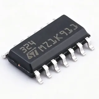
AD647SE/883B - Ultralow Drift Dual JFET Op Amp | Analog Devices
MPN: AD647SE/883B ✓ Active| Qty | Unit Price | Extended |
|---|---|---|
| 1 | $25.99 | $25.99 |
| 10 | $25.74 | $257.40 |
| 100 | $24.5 | $2,450.00 |
| 500 | $23 | $11,500.00 |
| 1,000 | $21.5 | $21,500.00 |
AD647SE/883B Overview
An operational amplifier (op amp) is a high-gain voltage amplifier with differential inputs and a single-ended output, used in analog signal processing. The AD647SE/883B is a dual op amp, meaning it contains two independent amplifiers in one package, saving board space and improving thermal tracking. As a JFET-input op amp, it offers very high input impedance and low bias current, ideal for interfacing with high-impedance sensors and precision integrators.
Key features include ultralow drift (typically 0.5 µV/°C), low noise, and high common-mode rejection. The device operates from dual supplies up to ±18 V, with a nominal supply voltage of 15 V. The extended temperature grade (S) supports operation from -55°C to +125°C, meeting military temperature requirements. The 20-lead CLCC package provides a compact, hermetic solution for harsh environments.
Technically, the AD647 uses ion-implantation and laser wafer drift trimming to achieve matched JFETs on a monolithic bipolar chip, resulting in superior DC precision. The device's bipolar technology ensures low offset voltage and drift, while the JFET input stage provides high input impedance. This combination makes it a versatile choice for precision analog circuits.
Typical applications include precision instrumentation amplifiers, active filters, data acquisition systems, and military avionics. Its low drift and high accuracy are critical in these applications where temperature variations can degrade performance.
When designing with the AD647SE/883B, ensure proper decoupling of the power supply pins with 0.1 µF ceramic capacitors close to the device. Also, consider the input bias current and offset voltage when designing high-impedance circuits, and use appropriate guarding techniques to minimize leakage currents.
Drop-in alternatives for AD647SE/883B — same package, pin-to-pin compatible. Different-package parts requiring PCB rework are excluded.
Quick Comparison Tool — Select alternative parts for side-by-side comparison:
AD647SE
✅ Drop-In📋 Reference alternative (not in catalog)
AD647SQ
✅ Drop-In ⚠️ Specs Unverified📋 Reference alternative (not in catalog)
AD647SE/883B Maximum Ratings & Electrical Characteristics
| Amplifier Type | Dual JFET Operational Amplifier |
| Number of Circuits | 2 |
| Input Offset Voltage (max) | 500 µV |
| Input Bias Current (max) | 10 pA |
| Slew Rate (min) | 2 V/µs |
| Supply Voltage (nominal) | 15 V |
| Supply Voltage Range | ±5 V to ±18 V |
| Max Negative Supply Voltage Limit | -18 V |
| Operating Temperature Range | -55°C to +125°C |
| Temperature Grade | Military |
| Package Type | 20-lead CLCC (9x9 mm) |
| Terminal Form | No Lead |
| Technology | Bipolar |
| MIL-STD-883B | Processed |
| RoHS | Compliant |
AD647SE/883B Pin Configuration
| Pin 1 | OUT A — Output of amplifier A |
| Pin 2 | -IN A — Inverting input of amplifier A |
| Pin 3 | +IN A — Non-inverting input of amplifier A |
| Pin 4 | V- — Negative supply voltage |
| Pin 5 | +IN B — Non-inverting input of amplifier B |
| Pin 6 | -IN B — Inverting input of amplifier B |
| Pin 7 | OUT B — Output of amplifier B |
| Pin 8 | V+ — Positive supply voltage |
| Pin 9 | NC — No connection |
| Pin 10 | NC — No connection |
| Pin 11 | NC — No connection |
| Pin 12 | NC — No connection |
| Pin 13 | NC — No connection |
| Pin 14 | NC — No connection |
| Pin 15 | NC — No connection |
| Pin 16 | NC — No connection |
| Pin 17 | NC — No connection |
| Pin 18 | NC — No connection |
| Pin 19 | NC — No connection |
| Pin 20 | NC — No connection |
Typical Applications
AD647SE/883B is suitable for 6 applications: Precision Instrumentation Amplifiers, Military Avionics Signal Conditioning, Data Acquisition Systems, Active Filters, Medical Monitoring Equipment, Industrial Process Control.
Precision Instrumentation Amplifiers
The AD647SE/883B's ultralow drift (0.5 µV/°C) and low input bias current (10 pA) make it ideal for precision instrumentation amplifiers. In a typical three-op-amp instrumentation amplifier configuration, the dual op amp provides the input stage with high common-mode rejection and low offset error. The military temperature range ensures stable performance in field-deployed test equipment. The JFET inputs minimize loading on high-impedance sensors, preserving signal integrity. With a slew rate of 2 V/µs, it can handle moderate-speed signals without distortion. The hermetic CLCC package protects against moisture and contamination, critical for long-term reliability in industrial and military environments.
Recommended
Military Avionics Signal Conditioning
In military avionics, the AD647SE/883B is used for signal conditioning of sensor outputs, such as accelerometers and gyroscopes. Its MIL-STD-883B processing ensures reliability under extreme vibration and temperature cycling. The dual op amp configuration saves board space in space-constrained avionics modules. The low offset voltage (500 µV max) and drift (0.5 µV/°C) maintain accuracy over the -55°C to +125°C range. The device's bipolar technology provides robust ESD performance, essential for harsh electromagnetic environments. The hermetic CLCC package offers superior protection against moisture and contaminants, extending service life in demanding applications.
Recommended
Data Acquisition Systems
The AD647SE/883B is well-suited for data acquisition systems where precision and low noise are paramount. Its low input bias current (10 pA) minimizes errors when driving high-impedance sources like photodiodes or pH sensors. The dual op amp can be used for anti-aliasing filtering and buffer stages in multi-channel systems. With a supply voltage range of ±5V to ±18V, it can interface with various ADC input ranges. The device's low offset voltage and drift ensure accurate conversion over temperature. The military temperature grade allows deployment in outdoor or unheated environments. The CLCC package's small footprint (9x9 mm) is advantageous for high-density PCB designs.
Recommended
Active Filters
The AD647SE/883B's high slew rate (2 V/µs) and low noise make it suitable for active filter designs, such as Butterworth or Chebyshev filters. The dual op amp allows implementation of second-order filter stages in a single package, reducing component count. The JFET inputs provide high input impedance, allowing the use of high-value resistors without loading effects. The device's low offset voltage minimizes DC errors in filter output. The military temperature range ensures stable filter characteristics across extreme conditions. The hermetic package is ideal for aerospace and defense filter applications where reliability is critical.
Recommended
Medical Monitoring Equipment
In medical monitoring, the AD647SE/883B can be used for ECG or EEG signal conditioning. Its low input bias current (10 pA) is essential for high-impedance electrode interfaces. The ultralow drift ensures stable baseline over time and temperature. The dual op amp configuration allows for right-leg drive and lead-off detection circuits in a compact design. The device's low noise performance helps maintain signal fidelity for accurate diagnosis. The military temperature range is overkill for medical applications, but the reliability of the hermetic package is beneficial for long-term implantable or portable devices. The RoHS compliance meets environmental regulations.
Recommended
Industrial Process Control
The AD647SE/883B is used in industrial process control for conditioning signals from transducers like pressure sensors and thermocouples. Its low offset voltage and drift ensure accurate measurement over long periods. The dual op amp can implement a two-stage amplifier or a bridge excitation and readout circuit. The wide supply range allows operation from common industrial rails (±15V). The military temperature range is suitable for harsh industrial environments. The hermetic CLCC package protects against dust, humidity, and corrosive gases. The device's high input impedance minimizes loading on sensors, preserving measurement accuracy.
Recommended
Recommended Products Summary
Engineering reference data for AD647SE/883B — comparison, design guidance, and compliance information.
Selection Guide
Comparison with Alternatives
| Parameter | This Product | AD647SE | AD647SQ | AD647JN |
|---|---|---|---|---|
| Package | 20-lead CLCC | 20-lead CLCC | 20-lead CLCC | 8-pin TO-99 |
| Brand | Analog Devices | Analog Devices | Analog Devices | Analog Devices |
| Input Offset Voltage (max) | 500 µV | 500 µV | 500 µV | 500 µV |
| Input Bias Current (max) | 10 pA | 10 pA | 10 pA | 10 pA |
| Slew Rate (min) | 2 V/µs | 2 V/µs | 2 V/µs | 2 V/µs |
| Supply Voltage Range | ±5V to ±18V | ±5V to ±18V | ±5V to ±18V | ±5V to ±18V |
| Operating Temperature Range | -55°C to +125°C | -55°C to +125°C | -55°C to +125°C | 0°C to +70°C |
| MIL-STD-883B | Yes | No | No | No |
Key Differentiators
- MIL-STD-883B processing (vs AD647SE)
- Hermetic CLCC package (vs AD647JN)
- Extended temperature range (vs AD647JN)
Design Notes
The AD647SE/883B operates from dual supplies up to ±18V. Ensure that the power supply is well-regulated and decoupled with 0.1µF ceramic capacitors placed close to the V+ and V- pins. For high-frequency noise, add a 10µF tantalum capacitor in parallel. The device's quiescent current is typically 3.5 mA per amplifier, so total power dissipation is low, but thermal management is still important in high-temperature environments.
For optimal performance, use a ground plane and keep input traces short and shielded. The high input impedance of the JFET inputs makes them susceptible to noise pickup, so guard rings around the input pins can reduce leakage currents. Place the feedback resistors close to the inverting input to minimize parasitic capacitance. The CLCC package has exposed pads; ensure proper soldering to the PCB for mechanical stability.
Do not exceed the absolute maximum supply voltage of ±18V, as this can damage the device. Also, avoid applying input voltages outside the supply rails, as this can cause latch-up. The input bias current is very low (10 pA), but it doubles for every 10°C increase in temperature, so account for this in high-temperature designs. Always use a socket or proper handling to avoid ESD damage, as the JFET inputs are sensitive.
Compliance Information
RoHS compliance confirmed by Veswin Electronics. MIL-STD-883B processing is a military standard, not a compliance certification.