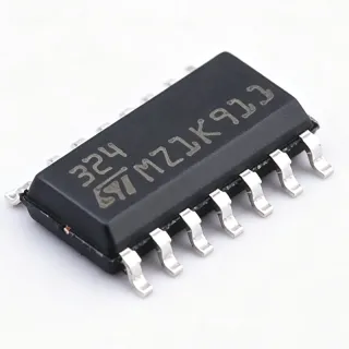
ADA4940-2ACPZ-RL7 - Ultralow Power ADC Driver | Analog Devices
MPN: ADA4940-2ACPZ-RL7 ✓ Active| Qty | Unit Price | Extended |
|---|---|---|
| 1 | $7.09 | $7.09 |
| 10 | $6.38 | $63.80 |
| 100 | $5.67 | $567.00 |
| 500 | $5.1 | $2,550.00 |
| 1,000 | $4.78 | $4,780.00 |
ADA4940-2ACPZ-RL7 Overview
A fully differential amplifier (FDA) is an operational amplifier with differential inputs and differential outputs, providing balanced signals that reject common-mode noise and even-order harmonics. FDAs are essential in precision data acquisition systems, where they convert single-ended signals to differential for driving ADCs, improving dynamic range and reducing distortion. The ADA4940-2 belongs to the ADA4940 family, which includes the single-channel ADA4940-1 and the dual ADA4940-2, both offering the same low noise and low distortion performance.
Key features include a low input voltage noise of 3.9 nV/√Hz, a spurious-free dynamic range (SFDR) of -110 dBc at 100 kHz, and a -3 dB bandwidth of 26 MHz. The output common-mode voltage is adjustable via a VOCM pin, allowing precise level shifting to match the ADC input range. The device also features a disable pin for power-down, reducing quiescent current to 10 µA, and an internal common-mode feedback loop that maintains output balance.
The ADA4940-2 uses a precision bipolar process with laser-trimmed thin-film resistors, achieving low DC offset (typically 50 µV) and excellent gain accuracy. Its differential output swing is rail-to-rail, and it can drive capacitive loads up to 10 pF without oscillation. The device is fully specified over the -40°C to +125°C temperature range, ensuring reliable operation in industrial and automotive environments.
Typical applications include driving SAR ADCs such as the AD7985 and AD7768, medical imaging systems, portable instrumentation, and communications receivers. The low power consumption and small footprint make it suitable for multi-channel data acquisition systems where board space and thermal budget are constrained.
When designing with the ADA4940-2, ensure proper supply decoupling with 0.1 µF and 10 µF capacitors close to the VCC and VEE pins. The VOCM pin should be driven by a low-impedance source to avoid common-mode errors. For optimal distortion, keep the feedback resistor values between 200 Ω and 1 kΩ and minimize parasitic capacitance at the summing nodes.
Drop-in alternatives for ADA4940-2ACPZ-RL7 — same package, pin-to-pin compatible. Different-package parts requiring PCB rework are excluded.
Quick Comparison Tool — Select alternative parts for side-by-side comparison:
ADA4940-2ACPZ-R7
✅ Drop-In📋 Reference alternative (not in catalog)
ADA4940-2ACPZ-RL
✅ Drop-In📋 Reference alternative (not in catalog)
ADA4950-2YCPZ-RL
✅ Drop-In ⚠️ Specs Unverified📋 Reference alternative (not in catalog)
THS4521
✅ Drop-In ⚠️ Specs Unverified📋 Reference alternative (not in catalog)
LTC6362
✅ Drop-In ⚠️ Specs Unverified📋 Reference alternative (not in catalog)
ADA4940-2ACPZ-RL7 Maximum Ratings & Electrical Characteristics
| Number of Channels | 2 |
| Supply Voltage Range | 3.3 V to 7 V (single), ±1.65 V to ±3.5 V (dual) |
| Quiescent Current per Amplifier | 1.25 mA |
| Input Voltage Noise | 3.9 nV/√Hz |
| SFDR | -110 dBc at 100 kHz |
| Bandwidth (-3 dB) | 26 MHz |
| Slew Rate | 50 V/µs |
| Output Common-Mode Range | Rail-to-rail |
| Input Offset Voltage | 50 µV (typical) |
| Input Bias Current | 1.5 µA |
| Output Current | 40 mA |
| Operating Temperature Range | -40°C to +125°C |
| Package | 24-Lead LFCSP (4mm x 4mm) |
| Mounting Type | Surface Mount |
| RoHS Status | Compliant |
| Lead-Free | Yes |
ADA4940-2ACPZ-RL7 Pin Configuration
| Pin 1 | OUT+ — Positive differential output |
| Pin 2 | VOCM — Output common-mode voltage set |
| Pin 3 | VEE — Negative supply (or ground) |
| Pin 4 | IN- — Inverting input |
| Pin 5 | IN+ — Non-inverting input |
| Pin 6 | VCC — Positive supply |
| Pin 7 | PD — Power-down (active low) |
| Pin 8 | OUT- — Negative differential output |
| Pin 9 | NC — No connect |
| Pin 10 | NC — No connect |
| Pin 11 | NC — No connect |
| Pin 12 | NC — No connect |
| Pin 13 | NC — No connect |
| Pin 14 | NC — No connect |
| Pin 15 | NC — No connect |
| Pin 16 | NC — No connect |
| Pin 17 | NC — No connect |
| Pin 18 | NC — No connect |
| Pin 19 | NC — No connect |
| Pin 20 | NC — No connect |
| Pin 21 | NC — No connect |
| Pin 22 | NC — No connect |
| Pin 23 | NC — No connect |
| Pin 24 | NC — No connect |
| Pin EP | Exposed Pad — Thermal pad, connect to ground |
Typical Applications
ADA4940-2ACPZ-RL7 is suitable for 6 applications: SAR ADC Driver, Sigma-Delta ADC Driver, Portable Instrumentation, Medical Imaging, Communications Receivers, Test and Measurement.
SAR ADC Driver
The ADA4940-2ACPZ-RL7 is optimized to drive low-power, high-resolution SAR ADCs such as the AD7985 and AD7768. Its ultralow quiescent current of 1.25 mA per channel preserves battery life in portable data acquisition systems. The low noise (3.9 nV/√Hz) and low distortion (-110 dBc SFDR) ensure the ADC achieves its specified SNR and THD. The adjustable output common-mode voltage allows direct interface to the ADC's input range, simplifying the design. With a bandwidth of 26 MHz, it supports sampling rates up to several MSPS without introducing significant settling errors.
Recommended
Sigma-Delta ADC Driver
For high-resolution sigma-delta ADCs like the AD7768, the ADA4940-2ACPZ-RL7 provides a clean differential signal with low noise and distortion. Its low power consumption is critical in multi-channel systems where many amplifiers are used. The device's rail-to-rail output swing maximizes the ADC's dynamic range, and the VOCM pin allows precise level shifting to match the ADC's common-mode voltage. The wide bandwidth ensures minimal phase shift at the ADC's modulation frequency, preserving signal integrity.
Recommended
Portable Instrumentation
In battery-powered instruments such as handheld multimeters and portable medical devices, the ADA4940-2ACPZ-RL7's ultralow power consumption extends battery life. Its small 4mm x 4mm LFCSP package saves board space, and the low noise ensures accurate measurement of small sensor signals. The device operates from a single 3.3V supply, simplifying power design. The disable pin allows power-down between measurements, reducing average current to microamps.
Recommended
Medical Imaging
The ADA4940-2ACPZ-RL7 is suitable for medical imaging systems such as ultrasound and MRI, where low noise and low distortion are paramount. Its differential output rejects common-mode interference from the imaging environment. The low power dissipation reduces heat in dense arrays, improving system reliability. The wide bandwidth supports high-speed signal processing, and the small package allows high channel density. The device's performance is consistent over the -40°C to +125°C range, ensuring stable operation in clinical settings.
Recommended
Communications Receivers
In communications receivers, the ADA4940-2ACPZ-RL7 drives ADCs that digitize IF or baseband signals. Its low distortion (-110 dBc SFDR) ensures that adjacent channel interference is not generated, maintaining receiver sensitivity. The low power consumption is beneficial in multi-channel base stations. The adjustable common-mode voltage allows interface to ADCs with different input ranges. The device's bandwidth of 26 MHz is sufficient for most IF frequencies, and its differential output reduces even-order harmonics.
Recommended
Test and Measurement
The ADA4940-2ACPZ-RL7 is used in test equipment such as oscilloscopes and spectrum analyzers to condition signals before ADC conversion. Its low noise and high bandwidth preserve signal fidelity, and the differential output improves common-mode rejection. The low power consumption is advantageous in portable test instruments. The device's small package allows compact designs, and its wide supply range accommodates various system rails. The disable pin enables power management in battery-operated equipment.
Recommended
Recommended Products Summary
Engineering reference data for ADA4940-2ACPZ-RL7 — comparison, design guidance, and compliance information.
Selection Guide
Comparison with Alternatives
| Parameter | This Product | ADA4940-2ACPZ-R7 | ADA4940-2ACPZ-RL | ADA4940-1ACPZ-R7 | ADA4950-2YCPZ-RL | THS4521 | LTC6362 |
|---|---|---|---|---|---|---|---|
| Package | 24-Lead LFCSP (4x4) | 24-Lead LFCSP (4x4) | 24-Lead LFCSP (4x4) | 16-Lead LFCSP (3x3) | 24-Lead LFCSP (4x4) | 24-Lead LFCSP (4x4) | 24-Lead LFCSP (4x4) |
| Brand | Analog Devices | Analog Devices | Analog Devices | Analog Devices | Analog Devices | Texas Instruments | Analog Devices |
| Number of Channels | 2 | 2 | 2 | 1 | 2 | 1 | 2 |
| Quiescent Current per Channel | 1.25 mA | 1.25 mA | 1.25 mA | 1.25 mA | 5 mA | 1.1 mA | 1.9 mA |
| Input Voltage Noise | 3.9 nV/√Hz | 3.9 nV/√Hz | 3.9 nV/√Hz | 3.9 nV/√Hz | 2.2 nV/√Hz | 4.6 nV/√Hz | 2.5 nV/√Hz |
| Bandwidth (-3 dB) | 26 MHz | 26 MHz | 26 MHz | 26 MHz | 500 MHz | 95 MHz | 180 MHz |
| SFDR | -110 dBc at 100 kHz | -110 dBc at 100 kHz | -110 dBc at 100 kHz | -110 dBc at 100 kHz | -90 dBc at 10 MHz | -100 dBc at 1 MHz | -120 dBc at 100 kHz |
| Supply Voltage Range | 3.3V to 7V | 3.3V to 7V | 3.3V to 7V | 3.3V to 7V | 3V to 5.25V | 2.5V to 5.5V | 2.8V to 5.25V |
Key Differentiators
- Ultralow quiescent current of 1.25 mA per channel (vs ADA4950-2YCPZ-RL)
- Lower noise than THS4521 (vs THS4521)
- Pin-compatible with ADA4950-2 in same package (vs ADA4950-2YCPZ-RL)
Design Notes
The ADA4940-2ACPZ-RL7 operates from a single 3.3V to 7V supply or dual supplies. For optimal performance, use low-ESR ceramic capacitors (0.1 µF and 10 µF) placed close to the VCC and VEE pins. The exposed pad should be connected to a low-impedance ground plane to aid thermal dissipation. In single-supply operation, ensure the input common-mode range is not violated by setting the VOCM appropriately.
For best distortion performance, keep the feedback resistor values between 200 Ω and 1 kΩ. Minimize parasitic capacitance at the summing nodes by placing resistors close to the inputs and using short traces. Use a solid ground plane under the device and avoid routing high-speed digital signals near the analog inputs. The exposed pad should be soldered to the PCB for thermal and electrical connection.
Do not leave the PD (power-down) pin floating; tie it high for normal operation or low to disable. The VOCM pin must be driven by a low-impedance source, such as a reference buffer, to avoid common-mode errors. Ensure the output common-mode voltage is within the ADC's input range to prevent clipping. Also, verify that the input signal does not exceed the absolute maximum ratings, as the device is not internally protected against overvoltage.
Compliance Information
RoHS compliant and lead-free per Analog Devices product page. Not AEC-Q100 qualified. Halogen-free status not specified in available data.