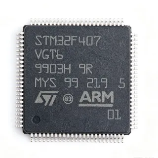
ATSAMG53N19A-AU - ARM Cortex-M4 48MHz MCU | Microchip
MPN: ATSAMG53N19A-AU ✓ Active| Qty | Unit Price | Extended |
|---|---|---|
| 1 | $1.6346 | $1.63 |
| 10 | $1.47 | $14.70 |
| 100 | $1.32 | $132.00 |
| 500 | $1.18 | $590.00 |
| 1,000 | $1.05 | $1,050.00 |
ATSAMG53N19A-AU Overview
A microcontroller (MCU) is a system-on-chip that integrates a CPU core, program memory (typically Flash), data memory (SRAM), and a rich set of peripherals into a single package. The ARM Cortex-M4 architecture adds a single-precision IEEE-754 floating-point unit and DSP extensions to the Cortex-M3 baseline, while maintaining deterministic interrupt latency (typically 12 cycles) and Thumb-2 instruction-set efficiency. Within the broader product taxonomy, the ATSAMG53N19A-AU belongs to the 32-bit MCU category, which itself is a subfamily of microcontrollers and a major branch of embedded processors alongside 8-bit MCUs (PIC, AVR) and DSPs.
Key features of this part include the 48 MHz Cortex-M4 core, hardware FPU, 512 KB on-chip Flash, 96 KB SRAM, an integrated 12-bit ADC, multiple USART/UART/SPI/TWI peripherals, USB 2.0 Full-Speed device with on-chip transceiver, up to 38 GPIO lines, and a 1.5 to 3.6 V supply range. An on-chip ultra-low-power RTC, multiple sleep modes, and a 32.768 kHz crystal oscillator enable battery-friendly designs. The 100-LQFP package provides ample I/O for industrial control panels and human-machine interface (HMI) front-ends.
Technically, the SAM G53 architecture pairs the Cortex-M4 core with a multi-layer AHB/APB bus matrix, a separate peripheral DMA controller (PDC), and a hardware cryptographic module on certain siblings. The 12-bit ADC achieves up to 1 MSPS sampling in single-ended mode, while the USB 2.0 Full-Speed peripheral and CAN controller provide connectivity options for industrial fieldbus and PC peripherals. The combination of low dynamic power consumption (under 1 mA/MHz at 1.8 V) and rapid wake-up from RTC alarm makes the part attractive for energy-constrained installations.
Typical applications include industrial control panels, building automation (HVAC, lighting), USB peripherals such as data loggers, motor control boards (BLDC, stepper), wireless sensor node baseboards, point-of-sale (POS) terminals, and consumer HMI touch-front panels. The industrial -40 to +85 C operating range suits factory-floor and outdoor enclosures.
When designing with this device, allocate the 48 MHz system clock carefully because the USB Full-Speed peripheral requires a 48 MHz ±0.25% reference, typically sourced from the 12 MHz main oscillator plus PLL. Power-supply decoupling must include at least a 1 uF bulk capacitor plus a 100 nF high-frequency bypass near each VDD/VDDIO pin pair, and the NRST line should include the recommended 100 nF capacitor to allow clean in-circuit resets. Plan Flash and SRAM budgets early because the 512 KB / 96 KB split is fixed and does not support external memory expansion on this LQFP-100 variant.
Drop-in alternatives for ATSAMG53N19A-AU — same package, pin-to-pin compatible. Different-package parts requiring PCB rework are excluded.
Variants in this series
Same-series models that are drop-in compatible with ATSAMG53N19A-AU (same form factor and footprint) — differing in Mounting Type, ADC, Core Architecture, Operating Temperature, Package.
Quick Comparison Tool — Select alternative parts for side-by-side comparison:
ATSAMG53N18A-AU
✅ Drop-In📋 Reference alternative (not in catalog)
ATSAMG51N18A-AU
✅ Drop-In📋 Reference alternative (not in catalog)
ATSAMG55N19A-AU
✅ Drop-In ⚠️ 参数待验证📋 Reference alternative (not in catalog)
ATSAME53N19A-AU
✅ Drop-In✓ In Stock
$5.4 / Unit
View Datasheet →ATSAME54N19A-AU
✅ Drop-In✓ In Stock
$5.42 / Unit
View Datasheet →ATSAMG53N19A-AU Maximum Ratings & Electrical Characteristics
| Core Architecture | ARM Cortex-M4 with FPU |
| Core Clock Speed | 48 MHz |
| Bit Width | 32-bit |
| Program Memory (Flash) | 512 KB (512K x 8) |
| RAM | 96 KB |
| Supply Voltage | 1.5 V to 3.6 V |
| Operating Temperature | -40 C to +85 C (Industrial) |
| Package | LQFP-100 (14x14 mm) |
| GPIO Count | Up to 38 |
| ADC | 12-bit, up to 1 MSPS |
| USB | USB 2.0 Full-Speed device with on-chip transceiver |
| Communication Peripherals | USART/UART/SPI/TWI/I2C |
| Oscillator | Internal 8 MHz, external 32.768 kHz RTC crystal support |
| Mounting Type | Surface Mount |
| MSL Level | 3 (per industry standard) |
| RoHS Status | Compliant |
ATSAMG53N19A-AU Pin Configuration
| Pin 1 | PB0 — General-purpose I/O / peripheral function (per SAM G53 datasheet pin table) |
| Pin 2 | PB1 — General-purpose I/O / peripheral function |
| Pin 3 | PB2 — General-purpose I/O / peripheral function |
| Pin 4 | PB3 — General-purpose I/O / peripheral function |
| Pin 5 | PB4 — General-purpose I/O / peripheral function |
| Pin 6 | PB5 — General-purpose I/O / peripheral function |
| Pin 7 | VDDIO — I/O supply voltage |
| Pin 8 | VSS — Ground |
| Pin 9 | PB6 — General-purpose I/O / peripheral function |
| Pin 10 | PB7 — General-purpose I/O / peripheral function |
| Pin 11 | PB8 — General-purpose I/O / peripheral function |
| Pin 12 | PB9 — General-purpose I/O / peripheral function |
| Pin 13 | PB10 — General-purpose I/O / peripheral function |
| Pin 14 | PB11 — General-purpose I/O / peripheral function |
| Pin 15 | PB12 — General-purpose I/O / peripheral function |
| Pin 16 | PB13 — General-purpose I/O / peripheral function |
| Pin 17 | PB14 — General-purpose I/O / peripheral function |
| Pin 18 | PB15 — General-purpose I/O / peripheral function |
| Pin 19 | VDDIO — I/O supply voltage |
| Pin 20 | VSS — Ground |
| Pin 21 | PC0 — General-purpose I/O / peripheral function |
| Pin 22 | PC1 — General-purpose I/O / peripheral function |
| Pin 23 | PC2 — General-purpose I/O / peripheral function |
| Pin 24 | PC3 — General-purpose I/O / peripheral function |
| Pin 25 | PC4 — General-purpose I/O / peripheral function |
| Pin 26 | PC5 — General-purpose I/O / peripheral function |
| Pin 27 | PC6 — General-purpose I/O / peripheral function |
| Pin 28 | PC7 — General-purpose I/O / peripheral function |
| Pin 29 | PC8 — General-purpose I/O / peripheral function |
| Pin 30 | PC9 — General-purpose I/O / peripheral function |
| Pin 31 | PC10 — General-purpose I/O / peripheral function |
| Pin 32 | PC11 — General-purpose I/O / peripheral function |
| Pin 33 | PC12 — General-purpose I/O / peripheral function |
| Pin 34 | PC13 — General-purpose I/O / peripheral function |
| Pin 35 | PC14 — General-purpose I/O / peripheral function |
| Pin 36 | PC15 — General-purpose I/O / peripheral function |
| Pin 37 | VDDIO — I/O supply voltage |
| Pin 38 | VSS — Ground |
| Pin 39 | PD0 — General-purpose I/O / peripheral function |
| Pin 40 | PD1 — General-purpose I/O / peripheral function |
| Pin 41 | PD2 — General-purpose I/O / peripheral function |
| Pin 42 | PD3 — General-purpose I/O / peripheral function |
| Pin 43 | PD4 — General-purpose I/O / peripheral function |
| Pin 44 | PD5 — General-purpose I/O / peripheral function |
| Pin 45 | PD6 — General-purpose I/O / peripheral function |
| Pin 46 | PD7 — General-purpose I/O / peripheral function |
| Pin 47 | PD8 — General-purpose I/O / peripheral function |
| Pin 48 | PD9 — General-purpose I/O / peripheral function |
| Pin 49 | PD10 — General-purpose I/O / peripheral function |
| Pin 50 | PD11 — General-purpose I/O / peripheral function |
| Pin 51 | PD12 — General-purpose I/O / peripheral function |
| Pin 52 | PD13 — General-purpose I/O / peripheral function |
| Pin 53 | PD14 — General-purpose I/O / peripheral function |
| Pin 54 | PD15 — General-purpose I/O / peripheral function |
| Pin 55 | VDDIO — I/O supply voltage |
| Pin 56 | VSS — Ground |
| Pin 57 | PA0 — General-purpose I/O / peripheral function |
| Pin 58 | PA1 — General-purpose I/O / peripheral function |
| Pin 59 | PA2 — General-purpose I/O / peripheral function |
| Pin 60 | PA3 — General-purpose I/O / peripheral function |
| Pin 61 | PA4 — General-purpose I/O / peripheral function |
| Pin 62 | PA5 — General-purpose I/O / peripheral function |
| Pin 63 | PA6 — General-purpose I/O / peripheral function |
| Pin 64 | PA7 — General-purpose I/O / peripheral function |
| Pin 65 | PA8 — General-purpose I/O / peripheral function |
| Pin 66 | PA9 — General-purpose I/O / peripheral function |
| Pin 67 | PA10 — General-purpose I/O / peripheral function |
| Pin 68 | PA11 — General-purpose I/O / peripheral function |
| Pin 69 | PA12 — General-purpose I/O / peripheral function |
| Pin 70 | PA13 — General-purpose I/O / peripheral function |
| Pin 71 | PA14 — General-purpose I/O / peripheral function |
| Pin 72 | PA15 — General-purpose I/O / peripheral function |
| Pin 73 | PA16 — General-purpose I/O / peripheral function |
| Pin 74 | PA17 — General-purpose I/O / peripheral function |
| Pin 75 | PA18 — General-purpose I/O / peripheral function |
| Pin 76 | PA19 — General-purpose I/O / peripheral function |
| Pin 77 | PA20 — General-purpose I/O / peripheral function |
| Pin 78 | PA21 — General-purpose I/O / peripheral function |
| Pin 79 | VDDIO — I/O supply voltage |
| Pin 80 | VSS — Ground |
| Pin 81 | PA22 — General-purpose I/O / peripheral function |
| Pin 82 | PA23 — General-purpose I/O / peripheral function |
| Pin 83 | PA24 — General-purpose I/O / peripheral function |
| Pin 84 | PA25 — General-purpose I/O / peripheral function |
| Pin 85 | PA26 — General-purpose I/O / peripheral function |
| Pin 86 | PA27 — General-purpose I/O / peripheral function |
| Pin 87 | PA28 — General-purpose I/O / peripheral function |
| Pin 88 | PA29 — General-purpose I/O / peripheral function |
| Pin 89 | PA30 — General-purpose I/O / peripheral function |
| Pin 90 | PA31 — General-purpose I/O / peripheral function |
| Pin 91 | VDDIO — I/O supply voltage |
| Pin 92 | VSS — Ground |
| Pin 93 | NRST — Reset input (active-low) |
| Pin 94 | TDI — JTAG Test Data In |
| Pin 95 | TMS — JTAG Test Mode Select |
| Pin 96 | TCK — JTAG Test Clock |
| Pin 97 | TDO — JTAG Test Data Out |
| Pin 98 | VDDCORE — Core supply (1.5-1.8 V) |
| Pin 99 | VSS — Ground |
| Pin 100 | VDDIO — I/O supply voltage |
Typical Applications
ATSAMG53N19A-AU is suitable for 6 applications: Industrial Control Panel / HMI Front-End, USB Data Logger / Sensor Bridge, Building Automation / HVAC Controller, BLDC Motor Drive Control Board, Point-of-Sale (POS) Terminal / Smart Card Reader, Wireless Sensor Network Base Node.
Industrial Control Panel / HMI Front-End
The ATSAMG53N19A-AU fits industrial control panels because its 48 MHz ARM Cortex-M4 with FPU executes graphical HMI stacks and fieldbus protocols within tight timing margins while keeping active power under 1 mA/MHz at 1.8 V. The 100-LQFP package delivers up to 38 GPIO lines for keypad scanning, LED matrices, and parallel TFT or segment LCD drive, while the 512 KB Flash accommodates full LVGL or emWin graphical stacks. Designers should expect to layer a 32.768 kHz RTC for time-stamped events and rely on the integrated 12-bit ADC for analog front-panel feedback (thermistor, potentiometer). This part is a typical Microchip Harmony 3 platform choice for PLCs and HMI panels in factory automation.
Recommended
USB Data Logger / Sensor Bridge
With on-chip USB 2.0 Full-Speed device and transceiver, the ATSAMG53N19A-AU plugs straight into a PC host for virtual-COM or MSC data logging without an external PHY, which trims BOM and PCB area. The 96 KB SRAM buffers sensor packets at 1 MSPS from the 12-bit ADC before they hit the USB endpoint FIFO, and the 512 KB Flash leaves room for a FATFS mass-storage stack plus user application code. Pair with the same 12 MHz crystal referenced through the PLL to meet USB timing accuracy. This is a common first-time Microchip Cortex-M4 design for test-and-measurement accessory designers.
Recommended
Building Automation / HVAC Controller
Building automation controllers benefit from the ATSAMG53N19A-AU's industrial -40 to +85 C temperature range and its low-power RTC/battery-domain wakeup. The Cortex-M4 with FPU runs PID loops for fan-coil and VAV (variable air volume) actuators at 48 MHz while staying inside the 1.5-3.6 V supply envelope of typical 24 VAC-wall-adapter-derived rails. Up to 38 GPIO lines handle relay drivers, triac firing zero-cross detectors, and 0-10 V analog outputs for legacy HVAC equipment. The 96 KB SRAM also accommodates BACnet or Modbus message buffers without external expansion.
Recommended
BLDC Motor Drive Control Board
The ATSAMG53N19A-AU's 12-bit 1 MSPS ADC and flexible PWM and timer peripherals make it suitable for sensored and sensorless BLDC motor control in PCB-mount drives up to a few hundred watts. Six PWM channels drive a three-phase bridge with hardware dead-time insertion, while the quadrature encoder interface feeds back rotor position for field-oriented control (FOC) algorithms accelerated by the Cortex-M4 FPU. The 100-LQFP package dissipates the typically small SAM G53 control-section power in open-air enclosures without a heatsink. For higher-power FOC or sinusoidal commutation, look at the SAM E70 family with its hardware Crypto and richer timer peripherals.
Recommended
Point-of-Sale (POS) Terminal / Smart Card Reader
POS terminals use the ATSAMG53N19A-AU's Cortex-M4 with FPU to handle display rendering, EMV smart-card communication, and USB-based printer transactions on a single chip. The 512 KB Flash fits a full USB-HID payment stack plus a graphical menu, and the 96 KB SRAM buffers merchant receipts in a small FATFS volume without spilling to external memory. The industrial temperature range tolerates the warm enclosure behind a backlit LCD, and the integrated 12-bit ADC reads battery-voltage and temperature sensors. Designers frequently pair this MCU with an external secure element for certified payment terminal builds.
Recommended
Wireless Sensor Network Base Node
Low-power wireless sensor base nodes use the ATSAMG53N19A-AU to gather frames from sub-GHz radios via SPI and repackage them onto USB or Ethernet uplinks. The 12-bit ADC samples board-level diagnostics while the UART/SPI peripherals drive common transceivers such as SAMD20-based remote nodes. Battery-friendly sleep modes plus a 32.768 kHz RTC enable wake-on-radio schemes where the gateway sleeps between scheduled polling intervals. For higher density or time-stamping accuracy, the SAM S70/E70 with hardware Ethernet MAC and richer timers offers a step up.
Recommended
Recommended Products Summary
Engineering reference data for ATSAMG53N19A-AU — comparison, design guidance, and compliance information.
Selection Guide
Comparison with Alternatives
| Parameter | This Product | ATSAMG53N18A-AU | ATSAMG51N18A-AU | ATSAMG55N19A-AU | ATSAME53N19A-AU | ATSAME54N19A-AU |
|---|---|---|---|---|---|---|
| Package | LQFP-100 (14x14 mm) | LQFP-100 (14x14 mm) - same | LQFP-100 (14x14 mm) - same | LQFP-100 (14x14 mm) - same | LQFP-100 (14x14 mm) - same | LQFP-100 (14x14 mm) - same |
| Brand | Microchip Technology | Microchip Technology | Microchip Technology | Microchip Technology | Microchip Technology | Microchip Technology |
| Core Architecture | ARM Cortex-M4 with FPU | ARM Cortex-M4 with FPU | ARM Cortex-M4 with FPU | ARM Cortex-M4 with FPU | ARM Cortex-M4F | ARM Cortex-M4F |
| Core Clock Speed | 48 MHz | 48 MHz | 48 MHz | 120 MHz | 120 MHz | 120 MHz |
| Flash Memory | 512 KB | 256 KB (-50%) | 256 KB (-50%) | 512 KB (same) | 512 KB (same) | 512 KB (same) |
| SRAM | 96 KB | 96 KB | 64 KB (-33%) | 96 KB | 128 KB (+33%) | 192 KB (+100%) |
| USB | USB 2.0 Full-Speed device | USB 2.0 Full-Speed device | USB 2.0 Full-Speed device | USB 2.0 OTG (Host/Device) | USB 2.0 Full-Speed + Ethernet | USB 2.0 High-Speed + CAN-FD |
| Operating Temperature | -40 to +85 C (Industrial) | -40 to +85 C | -40 to +85 C | -40 to +85 C | -40 to +85 C | -40 to +85 C |
Key Differentiators
- USB Full-Speed device with on-chip transceiver in 100-LQFP-100 (vs ATSAMG53N18A-AU)
- Cortex-M4 with FPU at 48 MHz in industrial temperature range (vs ATSAMG51N18A-AU)
- Pin-compatible upgrade path to 120 MHz SAM E5x family (vs ATSAME54N19A-AU)
Design Notes
Estimated: at 48 MHz CPU clock with USB Full-Speed active, the SAM G53's active current at 3.3 V is approximately 25 mA, so total power is roughly 80 mW. The 100-LQFP-14 has theta_JA on the order of 50 C/W, yielding a 4 C rise above ambient - well within the industrial 85 C ceiling. Place a 4.7 uF bulk + 100 nF bypass near each VDDCORE/VDDIO pin pair to stabilize core voltage during USB packet traffic.
Route USB DP / DM differential pair as 90-ohm differential over a continuous ground plane and keep the pair within 3 mm of the on-chip transceiver pins (PB10/PB11 in many SAM G53 GPIO maps). Place the 12 MHz crystal within 5 mm of the XTAL1/XTAL2 pins and use guard traces tied to ground. Avoid routing the JTAG signals (TCK/TMS/TDI/TDO) parallel to high-speed peripherals to ease boundary-scan diagnostics.
Do NOT use the internal 8 MHz RC oscillator when USB is enabled - USB Full-Speed requires the 12 MHz crystal plus PLL-derived 48 MHz reference within +/- 0.25%. Engineers new to the SAM G53 often forget to configure the PLL lockout window before enabling USB; this produces intermittent enumeration failures on cold starts. Likewise, watch for NRST bouncing if the reset capacitor is omitted - the part will reset again any time a 1.5 V supply glitch occurs during Flash programming.
Compliance Information
RoHS-compliant per Microchip product page; not AEC-Q100 qualified (industrial-grade only). Designers needing automotive AEC-Q100 should look at the SAM V71 or PIC32MX series.