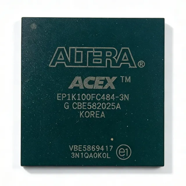
EP1K100FC484-3N - 100K-Gate ACEX 1K FPGA, 484-BGA | Intel
MPN: EP1K100FC484-3N ⚠ Last Time Buy| Qty | Unit Price | Extended |
|---|---|---|
| 1 | $139.58 | $139.58 |
| 10 | $124.5 | $1,245.00 |
| 100 | $95.2 | $9,520.00 |
| 500 | $78.4 | $39,200.00 |
| 1,000 | $65.1 | $65,100.00 |
EP1K100FC484-3N Overview
An FPGA (Field-Programmable Gate Array) is a programmable logic device that lets engineers implement arbitrary digital logic, signal-processing datapaths, glue logic, and embedded memory on a single chip after PCB fabrication. In the broader hierarchy, an FPGA sits above simple PAL/GAL SPLDs, above CPLDs, and below ASICs - it occupies the high-density, high-flexibility tier of programmable logic. The ACEX 1K family was Altera's first low-cost, die-efficient architecture that paired LUT-based logic with embedded memory, targeting system-on-a-programmable-chip (SOPC) designs.
Key features include 624 logic array blocks (LABs), 12 EABs providing 49,152 bits of embedded memory, multiVolt I/O support for interfacing with 2.5V, 3.3V, and 5V systems, JTAG-based IEEE 1149.1 boundary-scan test, in-system programmability via the passive serial configuration scheme, and a dedicated configuration circuitry. The 484-ball FBGA package supports 333 user I/O pins - among the highest in the ACEX 1K family - enabling wide parallel buses, multiple communication interfaces, and address/data multiplexing for external memory or bus peripherals.
Typical applications span telecommunications line cards, industrial control and factory automation, glue logic and bus bridging, glue-logic replacement of discrete 74-series logic, DSP pre/post-processing, and legacy ASIC prototyping. The combination of 100K ASIC gates of logic, dual-port RAM, and a 200 MHz internal fabric makes the EP1K100FC484-3N a practical choice for cost-sensitive volume production where an ASIC is not yet economical.
When designing with the EP1K100FC484-3N, plan the I/O bank voltage assignments early because the device supports 2.5V, 3.3V, and 5V interfaces through multiVolt I/O but requires careful reference-voltage planning. The configuration scheme (PS, JTAG, or PPA) must be selected before PCB layout, and decoupling capacitors must be placed within 100 mils of every VCCINT and VCCIO pin.
This page consolidates distributor pricing, same-brand drop-in equivalents, and ACEX 1K design considerations not available on a single manufacturer datasheet page, giving engineers a one-stop reference for sourcing and selecting this legacy FPGA.
Drop-in alternatives for EP1K100FC484-3N — same package, pin-to-pin compatible. Different-package parts requiring PCB rework are excluded.
Variants in this series
Same-series models that are drop-in compatible with EP1K100FC484-3N (same form factor and footprint) — differing in Process Technology, Speed Grade, Package, Configuration Method, RoHS Status.
Quick Comparison Tool — Select alternative parts for side-by-side comparison:
EP1K100FC484-3
✓ In Stock
$52.5 / Unit
View Datasheet →EP1K100FC484-2N
✓ In Stock
$58.4 / Unit
View Datasheet →EP1K100FC484-2
✓ In Stock
$33.4 / Unit
View Datasheet →EP1K100FC484-1N
✓ In Stock
$58.4 / Unit
View Datasheet →EP1K100FC484-1
✓ In Stock
$52.1 / Unit
View Datasheet →EP1K100FC256-3N
✓ In Stock
Contact for price
View Datasheet →EP1K100FC484-3N Maximum Ratings & Electrical Characteristics
| Family | ACEX 1K |
| Logic Elements | 4,992 |
| Typical Gate Count | 100,000 gates |
| Logic Array Blocks (LABs) | 624 |
| Embedded Array Blocks (EABs) | 12 |
| Total RAM Bits | 49,152 |
| User I/Os | 333 |
| Operating Voltage (VCCINT) | 2.5 V |
| Process Technology | 0.22 µm CMOS |
| Internal Operating Frequency | up to 200 MHz |
| Speed Grade | -3 |
| Package | 484-ball FBGA |
| Mounting Type | Surface Mount |
| Configuration Method | Passive Serial, JTAG, PPA |
| I/O Standards Supported | LVTTL, LVCMOS, PCI, 2.5V/3.3V/5V multiVolt I/O |
| Operating Temperature (Commercial) | 0 °C to +70 °C |
| Boundary-Scan Test | IEEE 1149.1 (JTAG) |
EP1K100FC484-3N 484-ball fbga Pin Configuration Guide
Pin configuration for EP1K100FC484-3N (484-ball fbga package). This digital IC includes GPIO, communication interfaces (UART, SPI, I2C), and power pins. Refer to the manufacturer datasheet for alternate pin functions and configuration options. Essential for embedded system design and PCB layout.

No detailed pinout data available for EP1K100FC484-3N.
Refer to the datasheet for full pin configuration.
Typical Applications
EP1K100FC484-3N is suitable for 6 applications: Industrial Control and Factory Automation, Telecommunications Line Cards and Channel Banks, Glue-Logic Replacement and Bus Bridging, DSP Pre/Post-Processing Coprocessor, ASIC Prototyping and Emulation, Legacy Defense and Avionics Avionics Interfaces.
Industrial Control and Factory Automation
The EP1K100FC484-3N fits industrial control and factory automation because its 333 user I/Os handle the wide parallel buses typical of PLC backplanes and its 49,152 RAM bits (12 EABs) buffer high-speed state-machine transitions in motor-control loops. The multiVolt I/O (2.5V/3.3V/5V) lets a single FPGA talk to legacy 5V sensors and modern 3.3V MCUs without level shifters. Its 200 MHz internal fabric is more than adequate for encoder decoding, PID loops, and EtherCAT/IP pre-processing.
Recommended
Telecommunications Line Cards and Channel Banks
In telecom line cards the EP1K100FC484-3N serves as a programmable framer, mapper, and glue-logic aggregator where its 100K-gate capacity easily absorbs multiple T1/E1 framers, HDLC controllers, and time-slot interchangers. The 12 EABs implement dual-port RAM FIFOs that buffer data between the network-side serializer and the backplane-side CPU without external SRAM, and JTAG (IEEE 1149.1) boundary scan simplifies board test on densely populated line cards.
Recommended
Glue-Logic Replacement and Bus Bridging
The EP1K100FC484-3N is ideal for replacing dozens of 74-series TTL buffers, latches, transceivers, and protocol converters with a single programmable device. Its 333 user I/Os easily replace an entire motherboard's worth of glue logic, while the 49,152 RAM bits provide asynchronous FIFOs for clock-domain crossing. Engineers frequently choose it to bridge legacy ISA, VME, or PCI buses to modern 3.3V processors in industrial and defense upgrades.
Recommended
DSP Pre/Post-Processing Coprocessor
The EP1K100FC484-3N is well suited as a DSP pre/post-processing coprocessor alongside a fixed-point DSP, where the FPGA handles FIR filters, FFT preambles, decimation, and data-routing glue that offload the DSP. Its 200 MHz internal fabric with 4,992 logic elements can typically sustain 8- or 16-tap FIRs at full audio/IF sample rates, while the embedded RAM blocks (49,152 bits) hold coefficient tables and delay lines without external SRAM.
Recommended
ASIC Prototyping and Emulation
The EP1K100FC484-3N remains useful as an ASIC prototype platform because 100K gates of LUT-based logic plus 12 EABs model the datapath and on-chip memory of a near-equivalent ASIC, allowing hardware/software co-validation before mask-set commitment. Its JTAG interface streamlines design iteration through ByteBlaster or USB-Blaster download cables, and multiVolt I/O eases interfacing to legacy ASIC test fixtures. Engineers typically use multiple ACEX 1K devices in parallel for larger ASIC partitions.
Recommended
Legacy Defense and Avionics Avionics Interfaces
The EP1K100FC484-3N serves in long-life defense and avionics platforms where equipment must remain supportable for decades and where its MIL-PRF-GDEE-810 heritage and 333 I/Os handle ARINC 429, MIL-STD-1553, and discrete interfaces simultaneously. The 12 EABs implement protocol FIFOs and the 2.5V core with 5V-tolerant I/O mixes cleanly with legacy bus drivers. Plan for last-time-buy lifecycle management - the part is mature, well-characterized, and available in industrial-temp variants.
Recommended
Recommended Products Summary
Engineering reference data for EP1K100FC484-3N — comparison, design guidance, and compliance information.
Selection Guide
Comparison with Alternatives
| Parameter | This Product | EP1K100FC484-3 | EP1K100FC484-2N | EP1K100FC484-2 | EP1K100FC484-1N | EP1K100FC484-1 | EP1K100FC256-3N |
|---|---|---|---|---|---|---|---|
| Package | 484-ball FBGA | 484-ball FBGA - same | 484-ball FBGA - same | 484-ball FBGA - same | 484-ball FBGA - same | 484-ball FBGA - same | 256-ball FBGA - different (smaller) |
| Brand | Intel (Altera) | Intel (Altera) - same | Intel (Altera) - same | Intel (Altera) - same | Intel (Altera) - same | Intel (Altera) - same | Intel (Altera) - same |
| Speed Grade | -3 (200 MHz) | -3 (200 MHz) - same | -2 (slower) | -2 (slower) | -1 (slowest) | -1 (slowest) | -3 (200 MHz) - same |
| Temperature Grade | Commercial (0 to +70 °C) | Industrial (-40 to +85 °C) | Commercial (0 to +70 °C) | Industrial (-40 to +85 °C) | Commercial (0 to +70 °C) | Industrial (-40 to +85 °C) | Commercial (0 to +70 °C) |
| User I/Os | 333 | 333 - same | 333 - same | 333 - same | 333 - same | 333 - same | 186 (-44%) |
| Logic Elements | 4,992 | 4,992 - same | 4,992 - same | 4,992 - same | 4,992 - same | 4,992 - same | 4,992 - same |
| Embedded RAM | 49,152 bits (12 EABs) | 49,152 bits - same | 49,152 bits - same | 49,152 bits - same | 49,152 bits - same | 49,152 bits - same | 49,152 bits - same |
| Operating Voltage (VCCINT) | 2.5 V | 2.5 V - same | 2.5 V - same | 2.5 V - same | 2.5 V - same | 2.5 V - same | 2.5 V - same |
| Lifecycle Status | Last-time-buy | Last-time-buy | Last-time-buy | Last-time-buy | Last-time-buy | Last-time-buy | Last-time-buy |
Key Differentiators
- Highest speed grade of the 484-FBGA ACEX 1K family (vs EP1K100FC484-2N)
- Commercial temperature grade for cost-sensitive volume deployment (vs EP1K100FC484-3)
- Full 333 I/O count for parallel buses (vs EP1K100FC256-3N)
Design Notes
The EP1K100FC484-3N requires a 2.5V ±5% VCCINT supply for the core logic and a separate VCCIO supply per I/O bank. Decoupling must include 0.1 µF ceramic capacitors within 100 mils of every VCCINT and VCCIO pin plus bulk 33 µF tantalum or polymer caps at the regulator outputs. Plan inrush current: configuration can briefly draw 1 A+ during initialization; ensure the 2.5V regulator has soft-start and that the bulk caps can hold the rail above 2.375V during configuration to prevent config failure.
FBGA escape routing is the critical layout challenge: the 484-ball FBGA uses 1.27 mm ball pitch (verify against the manufacturer package drawing). Use a 4-layer PCB minimum with two dedicated inner power/ground planes; route signal traces on the outer layers only when necessary. Pair the JTAG TCK pin with a 10 kΩ pull-up and TMS with a 10 kΩ pull-up per IEEE 1149.1 boundary-scan recommendations; leaving these floating causes intermittent JTAG failures. MultiVolt I/O banks require their VCCIO pins shorted together per bank - never mix 2.5V and 5V on the same bank.
Three common pitfalls: (1) Wrong configuration mode - verify whether MSEL0/2 pins select PS (passive serial) or PPA configuration; mismatched configuration devices cause silent startup failures. (2) Unused I/O bank power - any unused I/O bank must still have its VCCIO pin tied to a valid voltage; floating VCCIO produces indeterminate I/O behavior and excess leakage. (3) EAB misinterpretation - EABs can implement RAM, ROM, dual-port RAM, or FIFO, but only one mode per EAB; mixing modes across EABs requires Quartus design discipline.
Estimated: at maximum toggle activity (assume 50% of 333 I/Os toggling at 100 MHz, 10 pF loads), the EP1K100FC484-3N dissipates approximately 1.5 W. The 484-FBGA package has theta_JA of roughly 15 °C/W with a 4-layer PCB and 0 m/s airflow, so the junction temperature rises ~22 °C above ambient. Confirm with the manufacturer package thermal model for your board stack-up and derate for industrial (-40 °C to +85 °C) operation.
Compliance Information
Compliance flags (RoHS, lead-free, halogen-free) for this legacy Altera/Intel FPGA were not explicitly stated in the verified web data and are marked unknown. AEC-Q100 not applicable (FPGAs are not automotive-qualified discrete components; for automotive FPGA applications consider Cyclone IV or later).
