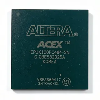
EP1K100FC484-2N - 100K Gates ACEX-1K FPGA 333 I/O 484-FBGA | Intel
MPN: EP1K100FC484-2N ⚠ Last Time Buy| Qty | Unit Price | Extended |
|---|---|---|
| 1 | $95 | $95.00 |
| 10 | $82.5 | $825.00 |
| 100 | $71.2 | $7,120.00 |
| 250 | $65 | $16,250.00 |
| 500 | $58.4 | $29,200.00 |
EP1K100FC484-2N Overview
An FPGA (Field-Programmable Gate Array) is a type of programmable logic device (PLD) containing an array of configurable logic blocks (CLBs), embedded memory blocks, and programmable interconnect, all defined by a user-loaded bitstream after manufacture. The ACEX-1K family sits within Intel's broader hierarchy of programmable logic: PLD -> CPLD/FPGA -> SRAM-based FPGA -> low-cost system-on-a-programmable-chip (SOPC) integration platform. Each logic element combines a 4-input look-up table, a programmable flip-flop, and a dedicated carry chain, while embedded array blocks (EABs) provide true dual-port RAM up to 16 bits wide.
Key features include 100K typical gates (49,152 RAM bits), 333 maximum user I/O, 250 MHz internal performance, JTAG-based in-system programmability via the IEEE 1149.1 boundary-scan interface, and built-in support for LVTTL, LVCMOS, PCI, SSTL-2/3, and GTL+ I/O standards. The -2 speed grade places this part in the mid-speed tier of the family, faster than -3 but slower than -1.
The ACEX-1K architecture provides enhanced embedded arrays for implementing megafunctions such as efficient memory and specialized peripheral interfaces. A fast continuous interconnect structure called the MultiCore architecture routes signals efficiently across the device, and dedicated clock pins feed global clock networks with low skew.
Typical applications include telecommunications glue logic, industrial control and instrumentation, low-cost glue logic for ASIC prototyping, video and image processing front-ends, network routers, and PCI bridge designs. The 333 I/O count makes it well suited to bus-intensive bridging tasks between microprocessors and peripherals.
When designing with this part, ensure that all I/O banks are powered from the correct VCCIO rail for the chosen I/O standard; mixing 3.3 V LVTTL with 2.5 V LVCMOS requires separate banks. The 484-FBGA package demands careful PCB layout with controlled-impedance traces and a minimum of four signal layers. Configuration via an EPC2 or EPC16 configuration device is recommended for production.
This page synthesizes distributor pricing, drop-in ACEX-1K alternatives, and design considerations not consolidated in the original datasheet.
Drop-in alternatives for EP1K100FC484-2N — same package, pin-to-pin compatible. Different-package parts requiring PCB rework are excluded.
Variants in this series
Same-series models that are drop-in compatible with EP1K100FC484-2N (same form factor and footprint) — differing in Process Technology, Package, Configuration Method, Speed Grade, RoHS Status.
Quick Comparison Tool — Select alternative parts for side-by-side comparison:
EP1K100FC484-2
✅ Drop-In✓ In Stock
$33.4 / Unit
View Datasheet →EP1K100FC484-1N
✅ Drop-In✓ In Stock
$58.4 / Unit
View Datasheet →EP1K100FC484-3N
✅ Drop-In✓ In Stock
$65.1 / Unit
View Datasheet →EP1K100FC484-1
✅ Drop-In✓ In Stock
$52.1 / Unit
View Datasheet →EP1K100EFI484-2
✅ Drop-In✓ In Stock
$67.5 / Unit
View Datasheet →EP1K100FI484-2
✅ Drop-In✓ In Stock
$118 / Unit
View Datasheet →EP1K100FC484-2N Maximum Ratings & Electrical Characteristics
| Family | ACEX-1K |
| Logic Elements | 4,992 |
| Typical Gates | 100,000 |
| Embedded Memory (EAB) | 49,152 bits |
| Maximum User I/O | 333 |
| Package | 484-ball FBGA |
| Core Voltage | 2.5 V |
| Process Technology | 0.22 µm SRAM |
| Speed Grade | -2 (commercial) |
| Mounting Type | Surface Mount |
| Configuration Method | SRAM, JTAG (IEEE 1149.1) |
| Programmable I/O Standards | LVTTL, LVCMOS, PCI, SSTL-2/3, GTL+ |
| Lead Status | Contains lead (legacy non-Pb-free suffix -2N) |
EP1K100FC484-2N 484-ball fbga Pin Configuration Guide
Pin configuration for EP1K100FC484-2N (484-ball fbga package). This digital IC includes GPIO, communication interfaces (UART, SPI, I2C), and power pins. Refer to the manufacturer datasheet for alternate pin functions and configuration options. Essential for embedded system design and PCB layout.

No detailed pinout data available for EP1K100FC484-2N.
Refer to the datasheet for full pin configuration.
Typical Applications
EP1K100FC484-2N is suitable for 6 applications: Telecommunications Glue Logic, Industrial Control and Instrumentation, ASIC Prototyping, PCI Bridge and Bus Interface, Video and Image Processing Front-End, Network Router and Switch Line-Card Logic.
Telecommunications Glue Logic
The EP1K100FC484-2N is well suited for telecom glue-logic bridging between network processors and PHY devices, where 333 user I/O pins provide ample wide-bus capacity for Utopia, POS-PHY, or SPI-4.2 interfaces. The 4,992 logic elements are sufficient to implement framer, deframer, and HDLC controllers on a single chip, while 49,152 bits of dual-port EAB RAM handle small packet buffers and look-up tables. The -2 speed grade's 250 MHz Fmax comfortably meets 155 MHz OC-3 and even some 622 MHz OC-12 datapath requirements when pipelined, eliminating the need for a separate ASIC. Pin-compatible migration to EP1K100FC484-1N is possible if timing margin is too tight.
Recommended
Industrial Control and Instrumentation
With 333 I/O and 4,992 logic elements, the EP1K100FC484-2N integrates motor-control loops, encoder interfaces, and Modbus/Profibus bridges in a single chip for PLCs and process controllers. The 0.22 µm process and 2.5 V core offer reliable operation across commercial ambient temperatures, while EAB-based dual-port RAM implements PID parameter tables and waveform lookups. The 484-FBGA footprint is footprint-compatible with the industrial-grade EP1K100EFI484-2 for designs that must be qualified to -40 °C to +100 °C. Altera's Quartus II design software supports the part with industrial reference designs for stepper and BLDC motor control.
Recommended
ASIC Prototyping
Engineers prototyping 100K-gate ASIC designs use the EP1K100FC484-2N to validate RTL before tape-out, because the ACEX-1K architecture supports deep, fast logic and 49 Kbits of dual-port RAM sufficient for most ASIC prototypes. The 333 I/O pins allow real-world external connections (memory, transceivers, ASIC pads), and JTAG-based in-system reprogrammability accelerates iteration cycles from hours (ASIC fab) to minutes (FPGA place-and-route). The -2 speed grade at 250 MHz internal gives realistic timing for many ASIC IP blocks. For larger ASICs (>150K gates), a Cyclone III or Cyclone IV device is the modern equivalent but requires a new PCB.
Recommended
PCI Bridge and Bus Interface
The EP1K100FC484-2N's 333 user I/O and built-in PCI I/O-standard support make it ideal for designing 32-bit/33 MHz PCI bridges between legacy microprocessors and PCI peripherals. The 4,992 logic elements can implement full target or master state machines, while the 49 Kbits of EAB RAM serves as scatter-gather DMA buffers and configuration-space registers. The 484-FBGA package provides the high pin density required for the 32-bit multiplexed PCI bus plus address and control signals. Designers should pair the FPGA with the ACEX-1K PCI MegaCore function from Altera to ensure protocol compliance.
Recommended
Video and Image Processing Front-End
The EP1K100FC484-2N's 250 MHz internal performance and 49,152 bits of dual-port RAM make it well suited for real-time video preprocessing tasks such as color-space conversion, deinterlacing, and frame-rate conversion at standard-definition resolutions. Its 333 I/O accommodate ITU-R BT.601/656 digital video buses plus memory interfaces to external SDRAM. The MultiCore interconnect fabric efficiently routes wide video datapaths (8-16 bits) without timing closure problems. For high-definition (HD) video, the -1 speed grade EP1K100FC484-1N provides additional margin. Quartus II includes reference designs for BT.656 input and VGA output interfaces.
Recommended
Network Router and Switch Line-Card Logic
The EP1K100FC484-2N is commonly used as forwarding-engine glue logic on router line cards, where its 333 I/O handle SPI-4.2, GMII, and RGMII interfaces between PHY and network processors. Its 4,992 logic elements support header parsing, checksum offload, and queue-management helpers, while dual-port EAB RAM implements small CAM/TCAM emulators and statistics counters. The 2.5 V core keeps power dissipation manageable in dense line-card layouts, and JTAG allows in-system firmware updates in the field. The pin-compatible industrial-grade EP1K100EFI484-2 variant supports outdoor cabinet deployments.
Recommended
Recommended Products Summary
Engineering reference data for EP1K100FC484-2N — comparison, design guidance, and compliance information.
Selection Guide
Comparison with Alternatives
| Parameter | This Product | EP1K100FC484-2 | EP1K100FC484-1N | EP1K100FC484-3N | EP1K100FC484-1 | EP1K100EFI484-2 |
|---|---|---|---|---|---|---|
| Brand | Intel (formerly Altera) | Intel | Intel | Intel | Intel | Intel |
| Package | 484-FBGA | 484-FBGA - same | 484-FBGA - same | 484-FBGA - same | 484-FBGA - same | 484-FBGA - same |
| Speed Grade | -2 (250 MHz Fmax) | -2 (250 MHz) | -1 (~300 MHz, faster) | -3 (~180 MHz, slower) | -1 (~300 MHz) | -2 (250 MHz) |
| Logic Elements | 4,992 | 4,992 | 4,992 | 4,992 | 4,992 | 4,992 |
| Typical Gates | 100K | 100K | 100K | 100K | 100K | 100K |
| Embedded Memory | 49,152 bits | 49,152 bits | 49,152 bits | 49,152 bits | 49,152 bits | 49,152 bits |
| Maximum User I/O | 333 | 333 | 333 | 333 | 333 | 333 |
| Core Voltage | 2.5 V | 2.5 V | 2.5 V | 2.5 V | 2.5 V | 2.5 V |
| Temperature Grade | Commercial | Commercial | Commercial | Commercial | Commercial | Industrial (-40C to +100C) |
| Lifecycle Status | Last-Time-Buy | Last-Time-Buy | Last-Time-Buy | Last-Time-Buy | Last-Time-Buy | Last-Time-Buy |
Key Differentiators
- Widest speed-grade flexibility in the EP1K100 FC484 family (vs EP1K100FC484-1N)
- Non-leaded (Pb-free) ball finish for RoHS compliance (vs EP1K100FC484-2)
- 333 user I/O - highest density in the ACEX-1K family (vs EP1K100FC256-2N (256-FBGA variant))
Design Notes
Estimated: at 250 MHz with 60% utilization, the EP1K100FC484-2N draws approximately 200-300 mA from the 2.5 V VCCINT rail and another 50-150 mA from the VCCIO rails depending on I/O switching activity. Designers must supply VCCINT from a low-noise LDO (e.g., TI TPS7A4533 or equivalent) decoupled with at least four 0.1 µF ceramic capacitors placed within 5 mm of the package. All VCCIO banks must be powered even if unused to prevent I/O leakage during SRAM configuration. Power-on sequencing requires VCCINT to reach 2.5 V before VCCIO to avoid latch-up.
The 484-FBGA package has 1.0 mm ball pitch and requires a minimum 4-layer PCB with continuous power and ground planes directly under the device. Per Altera's ACEX-1K hardware reference manual, signal traces should be length-matched within ±150 mils for buses wider than 16 bits, and all decoupling capacitors must be placed on the opposite side of the PCB directly beneath the BGA using via-in-pad or microvia technology. Thermal vias under the center balls are recommended for designs operating above 200 MHz with high utilization. JTAG chain connections (TCK, TMS, TDI, TDO) must be kept short and protected with 10 kΩ pull-ups on TCK and TMS.
Do not apply VCCIO before VCCINT during power-up - the ACEX-1K datasheet warns this can trigger permanent latch-up damage to I/O cells. A configuration device (EPC2 or EPC16) is mandatory in production because SRAM-based FPGAs lose their bitstream on power-down; relying on JTAG-only configuration is a common prototype-only mistake. The 'N' suffix denotes non-leaded (Pb-free) ball finish per Altera's part-number convention - confusing this with the leaded -2 (no N) variant may cause RoHS compliance failures in European markets. Cyclone family migration requires PCB rework because the BGA ball maps differ.
Compliance Information
Per Altera part-number convention, the 'N' suffix on EP1K100FC484-2N denotes non-leaded (Pb-free) ball finish variant; however, the core die and package assembly may still contain legacy materials subject to RoHS exemption 15 for lead-based die-attach. AEC-Q100 not applicable to FPGAs. REACH compliance not explicitly stated by Altera; assumed compliant based on legacy Intel/Altera documentation. Halogen-free and conflict-minerals status not documented in available data.