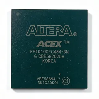
A3PE1500-FGG48I - 1.5M-Gate ProASIC3E Flash FPGA | Microchip
MPN: A3PE1500-FGG48I ✓ Active| Qty | Unit Price | Extended |
|---|---|---|
| 1 | $78.5 | $78.50 |
| 10 | $71.2 | $712.00 |
| 100 | $64.9 | $6,490.00 |
| 500 | $59.8 | $29,900.00 |
| 1,000 | $55.4 | $55,400.00 |
A3PE1500-FGG48I Overview
A flash-based FPGA is a field-programmable gate array that stores its configuration in on-chip flash memory cells rather than volatile SRAM. Unlike SRAM FPGAs, flash FPGAs are single-chip solutions: they configure instantly at power-up, require no external configuration PROM, and are inherently more secure because the bitstream is not stored in external memory. Within the programmable logic hierarchy, the A3PE1500 sits in Microchip's ProASIC3E family (600K to 3M system gates), positioned as a cost-effective ASIC replacement and complement to the Fusion mixed-signal family.
Key features include nonvolatile flash programming for instant-on operation, 130 nm flash process technology, reprogrammability for in-field updates, optional soft ARM support via the Cortex-M1 soft core, and abundant embedded memory. The ProASIC3E fabric also supports high-performance interfaces and offers a low total cost of ownership (TOC) per Microchip's product positioning.
Architecturally, the device is built on a 130 nm flash process with a sea-of-vanilla-gates style fabric, providing deterministic timing and single-chip secure configuration. The 484-ball FBGA gives dense signal access, supporting the full 280 user I/O count for wide bus interfaces and data-path designs.
Typical applications include networking and communications line cards, industrial control, avionics and military subsystems, consumer platforms, and ASIC prototyping or bridge logic, where the 1.5M-gate capacity and flash security matter.
Design consideration: as a 1.5V-core device, ensure proper power-rail sequencing and decoupling, and verify I/O bank voltage assignment against your interface standards in Libero SoC before routing.
This page synthesizes distributor listings, drop-in alternatives, and practical design notes not found in the manufacturer datasheet. Prices shown are as of 2026-09-02.
Drop-in alternatives for A3PE1500-FGG48I — same package, pin-to-pin compatible. Different-package parts requiring PCB rework are excluded.
Variants in this series
Same-series models that are drop-in compatible with A3PE1500-FGG48I (same form factor and footprint) — differing in System Gates, Package, Temperature Grade, Family, Speed Grade.
Quick Comparison Tool — Select alternative parts for side-by-side comparison:
A3PE1500-FGG484I
✅ Drop-In📋 Reference alternative (not in catalog)
A3PE1500-FGG484
✅ Drop-In📋 Reference alternative (not in catalog)
M1AFS1500-FGG484I
✅ Drop-In ⚠️ Specs Unverified✓ In Stock
$152.28 / Unit
View Datasheet →M1AFS1500-1FGG484I
✅ Drop-In ⚠️ Specs Unverified✓ In Stock
Contact for price
View Datasheet →M1AFS1500-2FGG484I
✅ Drop-In ⚠️ Specs Unverified✓ In Stock
$201.11 / Unit
View Datasheet →A3PE1500-FGG48I Maximum Ratings & Electrical Characteristics
| Family | ProASIC3E Flash FPGA |
| System Gates | 1500000 |
| User I/O | 280 |
| Maximum System Frequency | 231 MHz |
| Process Technology | 130 nm flash |
| Core Supply Voltage | 1.5 V |
| Configuration Memory | Nonvolatile flash (single-chip) |
| Package | 484-ball FBGA |
| Temperature Grade | Industrial (I) |
| Soft CPU Support | ARM Cortex-M1 soft core (optional) |
| Mounting Type | Surface Mount |
| Terminal Form | Ball |
| Reprogrammability | Yes (in-system flash reprogrammable) |
A3PE1500-FGG48I 484-ball fbga Pin Configuration Guide
Pin configuration for A3PE1500-FGG48I (484-ball fbga package). This digital IC includes GPIO, communication interfaces (UART, SPI, I2C), and power pins. Refer to the manufacturer datasheet for alternate pin functions and configuration options. Essential for embedded system design and PCB layout.

No detailed pinout data available for A3PE1500-FGG48I.
Refer to the datasheet for full pin configuration.
Typical Applications
A3PE1500-FGG48I is suitable for 6 applications: Networking and Communications, Industrial Automation and Control, Avionics and Defense Electronics, ASIC Prototyping and Bridge Logic, Consumer and Multimedia Platforms, Secure Embedded Systems.
Networking and Communications
The A3PE1500-FGG48I fits networking line cards, switch fabric glue logic, and protocol bridge designs where 1.5M gates and 280 user I/Os provide enough fabric for wide parallel data paths and interface conversion. According to Microchip's ProASIC3E positioning, the family targets the networking/communications market as a cost-effective ASIC replacement. The flash fabric's instant-on, single-chip configuration removes the external boot PROM that SRAM FPGAs require, shortening link bring-up time, while the 231 MHz system performance supports mainstream telecom clock domains. Industrial temperature grading suits remote cabinet and outdoor equipment.
Recommended
Industrial Automation and Control
In factory automation, motor-control supervisory logic, and industrial Ethernet bridges, the A3PE1500-FGG48I provides deterministic flash-based logic with industrial temperature qualification. The 1.5M-gate fabric implements state machines, encoders/decoders, and safety interlocks, while 280 I/Os interface PLC backplanes and sensor banks. Because configuration is stored on-chip in flash, a power cycle restores operation instantly without a boot sequence - critical in processes where downtime costs dominate. The FBGA's 484-ball footprint also supports legacy board reuse when upgrading from smaller ProASIC3 devices within the same family footprint strategy.
Recommended
Avionics and Defense Electronics
Microchip markets the ProASIC3E family for avionics applications, and the A3PE1500-FGG48I's flash configuration memory offers intrinsic SEU resilience advantages over SRAM configuration cells - there is no configuration bitstream in volatile memory to upset. The industrial-grade screening, 1.5M-gate capacity, and 231 MHz performance support mission computer glue logic, sensor interface aggregation, and actuator control paths. Single-chip, instant-on operation also satisfies avionics power-up latency requirements, and the absence of an external configuration device removes one failure mode and one potential bitstream-intercept point in secure platforms.
Recommended
ASIC Prototyping and Bridge Logic
As a 1.5M-gate flash FPGA on a 130 nm process, the A3PE1500-FGG48I is explicitly positioned by Microchip as a cost-effective ASIC replacement and prototyping vehicle. Design teams can implement ASIC front-end logic, verify interfaces, and ship low-volume bridge logic without NRE charges. The flash fabric permits in-field reprogramming for design fixes - unlike mask ASICs - while behaving like a hard-wired device at power-up. The 484-ball FBGA provides the high I/O count (280 user I/Os) needed to mirror wide ASIC pin interfaces during emulation and system bring-up.
Recommended
Consumer and Multimedia Platforms
The ProASIC3E datasheet identifies consumer markets as a primary target, and the A3PE1500-FGG48I serves set-top box glue logic, display interface bridging, and device aggregation where single-chip flash FPGAs cut bill-of-materials cost. Total cost of ownership (TOC) is a Microchip headline feature: no external configuration PROM, no controller firmware, and instant-on behavior reduce component count and assembly cost versus SRAM FPGA solutions. The 130 nm process delivers competitive die cost at 1.5M gates, and the 484-ball FBGA keeps board area compact for consumer enclosures.
Recommended
Secure Embedded Systems
Flash FPGAs are inherently more secure than SRAM FPGAs because the configuration bitstream never appears on an external bus - there is nothing to intercept during power-up. The A3PE1500-FGG48I therefore suits secure embedded controllers, authenticated peripherals, and anti-tamper platforms. Combined with optional ARM Cortex-M1 soft-core support on-chip, a single 1.5M-gate device can host both processor and custom cryptographic glue logic, eliminating a separate MCU and reducing the attack surface. Instant-on flash configuration also removes the boot window during which SRAM-based systems are vulnerable.
Recommended
Recommended Products Summary
Engineering reference data for A3PE1500-FGG48I — comparison, design guidance, and compliance information.
Selection Guide
Comparison with Alternatives
| Parameter | This Product | A3PE1500-FGG484I | A3PE1500-FGG484 | M1AFS1500-FGG484I | M1AFS1500-2FGG484I |
|---|---|---|---|---|---|
| Package | 484-ball FBGA | 484-ball FBGA - same | 484-ball FBGA - same | 484-ball FBGA - same | 484-ball FBGA - same |
| Brand | Microchip Technology (ProASIC3E) | Microchip Technology | Microchip Technology | Microchip Technology (Fusion) | Microchip Technology (Fusion) |
| System Gates | 1.5M | 1.5M | 1.5M | 1.5M | 1.5M |
| Temperature Grade | Industrial (I) | Industrial (I) | Commercial/standard | Industrial (I) | Industrial (I) |
| Configuration Memory | On-chip flash (single-chip) | On-chip flash | On-chip flash | On-chip flash + analog blocks | On-chip flash + analog blocks |
| Analog Peripherals | None (digital-only fabric) | None | None | ADC, voltage/temp monitors (Fusion) | ADC, voltage/temp monitors (Fusion) |
| Core Supply Voltage | 1.5 V | 1.5 V | 1.5 V | 1.5 V | 1.5 V |
Key Differentiators
- Single-chip instant-on flash configuration (vs SRAM-based FPGAs from other vendors)
- Identical-die drop-in availability (vs A3PE1500-FGG484I)
- Migration path to on-chip analog (vs M1AFS1500-FGG484I)
Design Notes
The A3PE1500 uses a 1.5V core supply; I/O banks are powered separately, so plan rail sequencing and per-bank decoupling early. Estimated: with 1.5M gates of flash fabric, static current is far lower than an equivalent SRAM FPGA, but dynamic current scales with clock frequency and toggle rate - budget bulk capacitance near each VCC bank (typically 10uF plus 0.1uF per pin group) and verify total rail current with Libero SoC power analysis before finalizing the DC-DC converter sizing.
The 484-ball FBGA requires a fine-pitch BGA land pattern and controlled escape routing. Follow IPC-standard BGA land geometry (building on the nominal 1.0 mm ball pitch typical for this package class) and use via-in-pad or dog-bone escapes on outer rows. Reserve at least two internal signal layers for BGA fanout and dedicate one plane to the 1.5V core with solid copper under the die to aid heat spreading. Confirm the exact mechanical drawing in the ProASIC3E datasheet (document 50003270B) before footprint release.
Do not confuse order codes: A3PE1500-FGG48I, A3PE1500-FGG484 and A3PE1500-FGG484I all refer to the same 484-ball FBGA device, but the presence or absence of the I suffix changes the temperature grade - substituting commercial grade into an industrial design compromises qualification. Also note that cross-brand FPGA substitution is never pin-compatible: migrating to another vendor requires PCB redesign and re-verification, so plan a second source within the Microchip ProASIC3E/Fusion families instead.
Compliance Information
Compliance data was not captured in the retrieved web data for this order code. Confirm RoHS/REACH certificates via the Microchip product page or distributor compliance documentation.