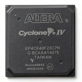
EP1K50FC484-3N - 50K Gates ACEX-1K FPGA 484-BBGA | Intel
MPN: EP1K50FC484-3N ✗ End of Life| Qty | Unit Price | Extended |
|---|---|---|
| 1 | $38.5 | $38.50 |
| 10 | $32.75 | $327.50 |
| 100 | $27.4 | $2,740.00 |
| 500 | $22.95 | $11,475.00 |
| 1,000 | $19.5 | $19,500.00 |
EP1K50FC484-3N Overview
What is an FPGA? A Field Programmable Gate Array (FPGA) is a class of programmable logic device that allows designers to configure arbitrary digital logic after PCB fabrication, sitting in the hierarchy between simple PLDs (CPLD) and fixed-function ASICs. ACEX-1K was Altera's first family to embed distributed dual-port SRAM blocks alongside the logic fabric, enabling single-chip system-on-a-programmable-chip (SOPC) designs that combine glue logic, FIFOs, and small processor interfaces without external memory.
Key features include 360 Logic Array Blocks (LABs), embedded array blocks (EABs) for efficient memory and specialized logic, in-system programmability via JTAG, and multi-voltage I/O support (1.8 V, 2.5 V, 3.3 V) on the same die. The device is supported by the Altera Quartus II MAX+PLUS II design software and is fully pin-compatible with other ACEX-1K 484-BGA speed grade variants, allowing drop-in PCB reuse when migrating between speed grades or density points within the same package.
Architecturally, ACEX-1K uses a continuous, sea-of-LABs routing fabric with dedicated carry chains for fast arithmetic and a MegaLAB structure that groups multiple LABs with a shared EAB. This gives the EP1K50FC484-3N a balanced logic-to-memory ratio for bus bridges, peripheral controllers, and telecom glue logic.
Typical applications span industrial control boards, telecommunications line cards, low-cost video/display controllers, glue logic between microprocessors and DSPs, and legacy system upgrades. Its 484-BGA footprint suits medium-complexity boards where higher-density Cyclone or Stratix devices would be overkill.
When designing with this part, note that ACEX-1K is a mature, end-of-life family - verify last-time-buy status before committing to new production. The 484-BBGA package requires careful PCB stack-up and via-in-pad or via-array escape routing; refer to the Altera ACEX-1K Device Family datasheet for recommended decoupling and JTAG chain guidance.
This page synthesizes distributor pricing, drop-in ACEX-1K family alternatives, and practical design notes not found in the manufacturer datasheet alone, helping engineers qualify the EP1K50FC484-3N for both new designs and legacy board refresh.
Drop-in alternatives for EP1K50FC484-3N — same package, pin-to-pin compatible. Different-package parts requiring PCB rework are excluded.
Variants in this series
Same-series models that are drop-in compatible with EP1K50FC484-3N (same form factor and footprint) — differing in Package, Speed Grade, Operating Temperature, Process Technology, Configuration Method.
Quick Comparison Tool — Select alternative parts for side-by-side comparison:
EP1K50FC484-3
✅ Drop-In✓ In Stock
$42.1 / Unit
View Datasheet →EP1K50FC484-2N
✅ Drop-In✓ In Stock
$26.4 / Unit
View Datasheet →EP1K50FC484-1N
✅ Drop-In✓ In Stock
$21.4 / Unit
View Datasheet →EP1K50FC484-2
✅ Drop-In✓ In Stock
$21.8 / Unit
View Datasheet →EP1K50FC484-1
✅ Drop-In✓ In Stock
$26.4 / Unit
View Datasheet →EP1K50FC484-3N Maximum Ratings & Electrical Characteristics
| Family | ACEX-1K |
| Logic Elements / Cells | 2880 |
| Typical Gates | 50,000 |
| Embedded Memory Bits | 40,960 bits |
| Logic Array Blocks (LABs) | 360 |
| Maximum User I/O | 249 |
| Maximum Operating Frequency | 166.67 MHz |
| Process Technology | 0.22 um CMOS |
| Core Supply Voltage | 2.5 V |
| I/O Voltage Support | 1.8 V / 2.5 V / 3.3 V |
| Package | 484-ball FineLine BGA (FBGA) |
| Speed Grade | -3 (commercial) |
| Programming Interface | JTAG (in-system programmable) |
| Design Software | Altera Quartus II / MAX+PLUS II |
| Operating Temperature | 0C to +70C (commercial) |
| RoHS Status | Unknown - confirm at order |
| Lead-Free / Halogen-Free | Unknown - confirm at order |
EP1K50FC484-3N 484-ball fineline bga (fbga) Pin Configuration Guide
Pin configuration for EP1K50FC484-3N (484-ball fineline bga (fbga) package). This digital IC includes GPIO, communication interfaces (UART, SPI, I2C), and power pins. Refer to the manufacturer datasheet for alternate pin functions and configuration options. Essential for embedded system design and PCB layout.

No detailed pinout data available for EP1K50FC484-3N.
Refer to the datasheet for full pin configuration.
Typical Applications
EP1K50FC484-3N is suitable for 6 applications: Industrial Control Glue Logic, Telecommunications Line Card Interface, Legacy DSP Bus Bridge, Video Display Controller / VGA Front-End, PCI Bus Interface / Embedded Controller Bridge, Test and Measurement Front-End.
Industrial Control Glue Logic
The EP1K50FC484-3N is well suited to industrial control boards where multiple microcontrollers, sensors, and actuator drivers must be bridged. Its 2,880 logic cells and 360 LABs provide enough capacity to implement multiple bus bridges (SPI to I2C, UART to parallel), encoder counters, and PWM generators in a single chip. The 249 available I/O pins allow direct interfacing to legacy 5 V-tolerant logic through external resistors, and the 40,960 bits of embedded dual-port RAM serve as FIFOs between asynchronous data domains. The 2.5 V core and 1.8/2.5/3.3 V I/O support enables mixed-voltage integration on the same PCB. ACEX-1K devices have a long track record in factory automation, making this part a familiar choice for legacy equipment refresh and long-life industrial designs.
Recommended
Telecommunications Line Card Interface
Telecommunications line cards frequently use ACEX-1K devices to implement HDLC controllers, TDM bus multiplexers, and framer glue logic between PHY devices and network processors. The EP1K50FC484-3N's 166.67 MHz internal Fmax supports TDM bit-clock rates up to E1/T1 with margin, and the embedded dual-port EAB memory provides small buffer FIFOs for clock-domain crossing. The 484-ball FBGA package supports the high pin count required to fan out to multiple E1/T1 ports and parallel datacom interfaces. In legacy telecom hardware, this part remains in service for protocol conversion and low-density channel aggregation where a low-cost, mature FPGA is preferred over a newer Cyclone-class device.
Recommended
Legacy DSP Bus Bridge
The EP1K50FC484-3N is commonly deployed as a glue-logic bridge between legacy DSPs (such as TI TMS320C6x), microprocessors, and peripheral ASICs. Its 2,880 logic cells are sufficient to implement host-port interfaces (HPI), DMA engines, and memory-mapped register decoding. The 40,960 embedded RAM bits can host small instruction traces or look-up tables for signal-processing pre-conditioning. The 1.8/2.5/3.3 V I/O flexibility enables direct connection to 1.8 V DSP cores, 2.5 V ASICs, and 3.3 V memory buses on the same board, eliminating external level shifters and reducing BOM cost. The 484-ball FBGA provides ample I/O for 32-bit data buses plus address and control signals.
Recommended
Video Display Controller / VGA Front-End
Low-cost video front-ends and VGA/LCD timing generators have historically used ACEX-1K FPGAs. The EP1K50FC484-3N can implement a complete CRT/LCD timing controller, color-palette RAM, and simple 2D graphics engine within its 50K-gate budget. The 40,960 bits of embedded dual-port RAM are well-matched to a 256x16 color palette or a single scan-line buffer. The 166.67 MHz internal Fmax easily supports 25 MHz pixel clocks at 640x480 and even modest 1024x768 timings. The 249 user I/Os are sufficient for 24-bit color plus sync, blanking, and clock distribution. Industrial display integrators continue to qualify this part for long-life, low-volume display products.
Recommended
PCI Bus Interface / Embedded Controller Bridge
The EP1K50FC484-3N has been widely used to implement 32-bit, 33 MHz PCI target and master interfaces for embedded systems, particularly for retrocomputing, industrial PCs, and medical imaging boards. The 50K-gate capacity is sufficient to add a PCI core plus user-defined register space and DMA logic in a single device. The 1.8/2.5/3.3 V I/O support is compatible with the 3.3 V PCI signaling environment used on most modern motherboards. With 40,960 bits of embedded RAM, designers can host small FIFOs for PCI bus-master DMA transfers. The 484-ball FBGA accommodates the 49-pin PCI bus plus extensive user-defined I/O, making this part a common choice for PCI add-in cards still in production for industrial and test equipment.
Recommended
Test and Measurement Front-End
Test and measurement instruments often require custom front-end logic that does not fit a standard microcontroller. The EP1K50FC484-3N provides a flexible platform to implement protocol-aware stimulus generators, pattern detectors, and time-to-digital converters alongside dedicated ADC/DAC interfaces. Its 2,880 logic cells and 360 LABs are sufficient to host a soft-CPU core (such as a 16-bit Altera Nios variant) plus custom measurement logic. The 40,960 bits of embedded RAM serve as capture buffers or histogram memory. With 249 user I/O pins, the device can interface to multiple parallel ADCs, DACs, and front-panel connectors in bench-top instrumentation. ACEX-1K's long-term availability on the legacy market makes it viable for long-life, low-volume measurement products.
Recommended
Recommended Products Summary
Engineering reference data for EP1K50FC484-3N — comparison, design guidance, and compliance information.
Selection Guide
Comparison with Alternatives
| Parameter | This Product | EP1K50FC484-3 | EP1K50FC484-2N | EP1K50FC484-1N | EP1K50FC484-2 | EP1K50FC484-1 |
|---|---|---|---|---|---|---|
| Brand | Intel | Intel | Intel | Intel | Intel | Intel |
| Package | 484-ball FBGA | 484-ball FBGA - same | 484-ball FBGA - same | 484-ball FBGA - same | 484-ball FBGA - same | 484-ball FBGA - same |
| Speed Grade | -3 (commercial) | -3 | -2 | -1 | -2 | -1 |
| Typical Gates | 50,000 | 50,000 | 50,000 | 50,000 | 50,000 | 50,000 |
| Logic Cells | 2,880 | 2,880 | 2,880 | 2,880 | 2,880 | 2,880 |
| Embedded RAM Bits | 40,960 | 40,960 | 40,960 | 40,960 | 40,960 | 40,960 |
| Max User I/O | 249 | 249 | 249 | 249 | 249 | 249 |
| Max Internal Frequency | 166.67 MHz | 166.67 MHz | ~140-150 MHz | ~120-130 MHz | ~140-150 MHz | ~120-130 MHz |
| Core Voltage | 2.5 V | 2.5 V | 2.5 V | 2.5 V | 2.5 V | 2.5 V |
| Packaging | Tape & Reel | Tray | Tape & Reel | Tape & Reel | Tray | Tray |
Key Differentiators
- Fastest speed grade in the ACEX-1K 50K-gate family at 166.67 MHz (vs EP1K50FC484-2N)
- Tape-and-reel packaging for high-volume automated assembly (vs EP1K50FC484-3)
- Same 484-ball FBGA footprint as EP1K30 and EP1K100 family members (vs EP1K30FC256-3N)
Design Notes
The 484-ball FineLine BGA package requires a multilayer PCB with microvia or via-in-pad escape routing. Recommended stack-up is 8-12 layers with 1 oz copper outer layers and dedicated power planes for VCCINT (2.5 V) and VCCIO (per-bank). Place at least 8-12 decoupling capacitors (0.1 uF X7R) around the BGA perimeter, plus 4.7 uF bulk capacitors on each supply rail within 25 mm of the package. Follow Altera's AN75 (ACEX-1K Hardware Design Guidelines) for the recommended footprint and paste-stencil aperture ratios.
Do NOT attempt to compile ACEX-1K designs in modern Quartus Prime - ACEX-1K support was dropped after Quartus II v13.0sp1. Retain a legacy Quartus II installation for bitstream generation, or use MAX+PLUS II for older projects. Also verify the configuration mode (PS, AS, JTAG) matches your EPC configuration device; ACEX-1K uses older EPC1/EPC2 configuration memories, not the modern EPCQ series used by Cyclone devices.
Estimated: at typical ACEX-1K utilization (~70% logic, 100% EAB) with 166.67 MHz toggling, the 484-ball FBGA dissipates roughly 1.5-2.0 W. With the FBGA's typical theta_JA of ~15-18 C/W (4-layer JEDEC test board), junction temperature rise above ambient is ~25-35 C. In a sealed industrial enclosure, ensure at least 100 LFM of forced airflow across the BGA, or specify an industrial-temperature grade variant (-1 or -2 with extended temp range) if available.
Compliance Information
ACEX-1K is a legacy family. RoHS/REACH compliance status depends on the specific date/lot code - confirm with distributor at order time. AEC-Q100 not applicable for commercial-grade FPGA.