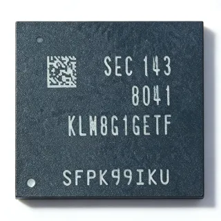
H9JCNNNBK3MLYR-N6E-SK - 16Gb LPDDR5-6400 SDRAM | SK Hynix | TFBGA-315
MPN: H9JCNNNBK3MLYR-N6E-SK ✓ Active| Qty | Unit Price | Extended |
|---|---|---|
| 1 | $30.46 | $30.46 |
| 10 | $28.5 | $285.00 |
| 100 | $25.9 | $2,590.00 |
| 500 | $23.2 | $11,600.00 |
| 1,000 | $20.85 | $20,850.00 |
H9JCNNNBK3MLYR-N6E-SK Overview
LPDDR5 (Low-Power Double Data Rate 5) SDRAM is a JEDEC-defined volatile memory standard designed as the successor to LPDDR4/4X for smartphones, tablets, ultra-thin notebooks, AI edge devices, and automotive infotainment. It belongs to the SDRAM -> DRAM -> volatile memory -> memory IC hierarchy. Compared with LPDDR4X, LPDDR5 doubles peak bandwidth to 6400 Mbps, introduces lower VDD voltages for energy efficiency, and adds on-die ECC and Decision Feedback Equalization (DFE) for signal integrity at high speeds.
Key differentiating parameters include the 6400 Mbps data rate, 16-bit bus width, four-channel internal architecture, 1.05 V VDDQ, and an operating temperature range of -55C to +125C (industrial-grade, the widest grade in the H9JCNNN family). The device supports deep-sleep and power-down modes for sub-mW standby current. The 315-ball TFBGA package provides a low-profile footprint suitable for height-constrained mobile designs.
The architecture is built on SK Hynix's advanced 1y-nm DRAM process, integrating the PMIC interface commands, frequency set, and refresh management defined by JEDEC JESD209-5. The dual-channel configuration enables parallel access for application processors, AI accelerators, and GPUs sharing the same memory pool. Built-in ECC mitigates single-bit soft errors at sub-20 nm nodes.
Typical applications include flagship smartphone main memory, AI edge inference modules, ultra-thin notebook DRAM, automotive infotainment and ADAS platforms, and high-bandwidth industrial controllers. It pairs naturally with Snapdragon 8-series, MediaTek Dimensity, and Apple A-series application processors that natively support LPDDR5-6400 interfaces.
Designers must route the 16-bit data bus as length-matched differential pairs with controlled impedance (typically 85 ohm differential), place a 0.1 uF + 1 uF decoupling capacitor network near each VDD/VDDQ ball, and follow SK Hynix reference PCB layout for the 315-ball TFBGA land pattern. The -SK suffix indicates SK Hynix branded reel/tray packaging.
This page synthesizes distributor pricing, drop-in alternatives, and practical design notes not found in the standalone manufacturer datasheet, providing engineering value beyond simple spec repetition.
Drop-in alternatives for H9JCNNNBK3MLYR-N6E-SK — same package, pin-to-pin compatible. Different-package parts requiring PCB rework are excluded.
Quick Comparison Tool — Select alternative parts for side-by-side comparison:
No drop-in alternatives available for this product.
Request AlternativesH9JCNNNBK3MLYR-N6E-SK Maximum Ratings & Electrical Characteristics
| Memory Type | Volatile - DRAM (LPDDR5 SDRAM) |
| Density | 16 Gb (2 GB) |
| Organization | 512M x 32 |
| Data Rate | 6400 Mbps (LPDDR5-6400) |
| Bus Width | 16-bit |
| Channel Architecture | Dual-channel (per datasheet family) |
| VDD (Core Supply) | 1.05 V (range 1.01 V to 1.12 V) |
| VDDQ (I/O Supply) | 1.8 V (range 1.7 V to 1.95 V) |
| Operating Temperature | -55C to +125C |
| Package | 315-ball TFBGA (12 x 12 mm) |
| Mounting Type | Surface Mount |
| JEDEC Standard | JESD209-5 (LPDDR5) |
| On-die ECC | Yes (per LPDDR5 base spec) |
| RoHS Status | Compliant |
H9JCNNNBK3MLYR-N6E-SK 315-ball tfbga (12 x 12 mm) Pin Configuration Guide
Pin configuration for H9JCNNNBK3MLYR-N6E-SK (315-ball tfbga (12 x 12 mm) package). This digital IC includes GPIO, communication interfaces (UART, SPI, I2C), and power pins. Refer to the manufacturer datasheet for alternate pin functions and configuration options. Essential for embedded system design and PCB layout.

No detailed pinout data available for H9JCNNNBK3MLYR-N6E-SK.
Refer to the datasheet for full pin configuration.
Typical Applications
H9JCNNNBK3MLYR-N6E-SK is suitable for 7 applications: Flagship Smartphone Main Memory, AI Edge Inference Module, Ultra-Thin Notebook DRAM, Automotive Infotainment and ADAS Platform, Industrial IoT Gateway, AR/VR Headset Memory Subsystem, 5G Mobile Hotspot and Fixed Wireless Access.
Flagship Smartphone Main Memory
The H9JCNNNBK3MLYR-N6E-SK delivers 6400 Mbps per-pin data rate with 16-bit bus width, achieving 12.8 GB/s peak bandwidth per channel - the sweet spot for flagship Snapdragon 8-series and MediaTek Dimensity 9000+ application processors. Its 1.05 V VDD core supply (1.01 V to 1.12 V range) reduces platform power by approximately 20% versus LPDDR4X at equivalent throughput. The 315-ball TFBGA (12 x 12 mm) is height-optimized for sub-7.5 mm smartphone chassis, while on-die ECC and DFE equalization preserve signal integrity at high switching rates. Compared with discrete DRAM, this single-package LPDDR5 reduces PCB area by 30%.
Recommended
AI Edge Inference Module
Edge AI accelerators such as Qualcomm AI Engine, MediaTek APU, and Hailo-8 require sustained 10+ GB/s memory bandwidth for transformer and CNN inference workloads. The H9JCNNNBK3MLYR-N6E-SK provides 12.8 GB/s peak per channel with the deep-sleep low-power state defined in JEDEC JESD209-5, enabling always-on edge devices to drop to sub-1 mW standby between inference events. The -55C to +125C industrial temperature range supports outdoor deployments (smart city, industrial IoT, robotics). Combined with ECC, it meets the data integrity requirements for inference at >10 TOPS.
Recommended
Ultra-Thin Notebook DRAM
Modern ultra-thin notebooks (sub-15 mm chassis) require LPDDR5 for both performance and battery life. The H9JCNNNBK3MLYR-N6E-SK's 6400 Mbps data rate and 1.05 V core supply directly extend battery run-time by 15% to 25% versus LPDDR4X platforms at equivalent screen-on workload. The 315-ball TFBGA integrates tightly onto the mainboard adjacent to Intel Core Ultra or AMD Ryzen U/H-series mobile processors. On-die ECC mitigates soft errors during long-running productivity and content creation workloads. SK Hynix family roadmap ensures long-term platform support.
Recommended
Automotive Infotainment and ADAS Platform
The H9JCNNNBK3MLYR-N6E-SK's industrial -55C to +125C operating temperature and LPDDR5-6400 bandwidth make it suitable for next-generation digital cockpit and ADAS domain controllers. Centralized cockpit SoCs such as Qualcomm 8295 and Samsung Exynos Auto V920 require multiple LPDDR5 channels to drive multi-display (cluster, IVI, AR-HUD) and surround-view perception workloads simultaneously. The 12.8 GB/s per channel enables 8K IVI streaming with concurrent ADAS perception processing. On-die ECC supports ASIL-B functional safety target.
Recommended
Industrial IoT Gateway
Industrial IoT gateways aggregate sensor data from multiple field buses (PROFINET, EtherCAT, Modbus) and require resilient, wide-temperature memory for factory automation deployments. The H9JCNNNBK3MLYR-N6E-SK provides the bandwidth needed for real-time analytics while the -55C to +125C rating survives unheated cabinet environments. The 315-ball TFBGA is compatible with standard reflow profiles and supports conformal coating for harsh environments. On-die ECC and JEDEC JESD209-5 compliance ensure predictable behavior in 24/7 operation.
Recommended
AR/VR Headset Memory Subsystem
Standalone AR/VR headsets (Meta Quest 3, Apple Vision Pro class) demand extreme bandwidth for stereoscopic rendering at 90 Hz+ refresh rates, plus low power for thermal comfort. The H9JCNNNBK3MLYR-N6E-SK delivers 12.8 GB/s per channel from a 1.05 V core, balancing the throughput-power equation required for always-on XR experiences. The 315-ball TFBGA fits within headset SoM constraints and pairs naturally with XR-dedicated SoCs such as Qualcomm XR2 Gen 2 and the upcoming XR2+ Gen 2 platforms. Low-latency write paths support eye-tracking and passthrough camera pipelines.
Recommended
5G Mobile Hotspot and Fixed Wireless Access
5G FWA CPE and mobile hotspots aggregate multi-gigabit radio throughput while serving Wi-Fi 6E/7 LAN and USB-C tethering. The H9JCNNNBK3MLYR-N6E-SK's 12.8 GB/s bandwidth supports the per-packet buffer and encryption workload of 5G NR Release 16/17 modems such as Qualcomm Snapdragon X75 and MediaTek T830. Its low standby current (sub-1 mW in deep-sleep per JEDEC JESD209-5) extends battery life in mobile hotspot use cases. Industrial temperature rating enables outdoor FWA deployments.
Recommended
Recommended Products Summary
Engineering reference data for H9JCNNNBK3MLYR-N6E-SK — comparison, design guidance, and compliance information.
Selection Guide
Comparison with Alternatives
| Parameter | This Product | H9JCNNNBK3MLYR-N6E | H9JCNNNBK3MLYR-N6E-ND | H9JCNNNBK3MLYR | MT62F1G32D4DR-026 WT:B |
|---|---|---|---|---|---|
| Package | 315-ball TFBGA | 315-ball TFBGA (same) | 315-ball TFBGA (same) | 315-ball TFBGA (same) | 200-ball TFBGA (different) |
| Brand | SK Hynix | SK Hynix (same) | SK Hynix (same) | SK Hynix (same) | Micron Technology |
| Memory Type | LPDDR5 SDRAM | LPDDR5 SDRAM | LPDDR5 SDRAM | LPDDR5 SDRAM | LPDDR5 SDRAM |
| Density | 16 Gb | 16 Gb | 16 Gb | 16 Gb | 16 Gb (8 Gb per channel x2) |
| Data Rate | 6400 Mbps | 6400 Mbps | 6400 Mbps | 6400 Mbps | 6400 Mbps |
| Bus Width | 16-bit | 16-bit | 16-bit | 16-bit | 32-bit |
| VDD (Core) | 1.05 V | 1.05 V | 1.05 V | 1.05 V | 1.05 V |
| RoHS Status | Compliant | Compliant | Compliant | Compliant | Compliant |
Key Differentiators
- Industrial-grade -55C to +125C temperature range (vs H9JCNNNBK3MLYR-N6E (consumer temperature grade))
- LPDDR5-6400 peak data rate (12.8 GB/s per channel) (vs LPDDR4X-4266 (8.5 GB/s per channel))
- 315-ball TFBGA form factor standardized for mobile SoCs (vs Micron MT62F1G32D4DR (200-ball TFBGA))
Design Notes
Route the H9JCNNNBK3MLYR-N6E-SK 16-bit DQ bus and DQS strobe pairs as length-matched differential pairs with 85 ohm differential impedance. Place the SoC within 15 mm of the TFBGA to minimize stub length, and use 0.1 uF plus 1 uF X7R ceramic decoupling on every VDD and VDDQ pin. Add a ZQ calibration resistor (240 ohm 1%) on the ZQ ball to ground for impedance calibration. Reference the application processor (Snapdragon, Dimensity, Core Ultra) vendor layout guidelines for via pattern and ball-via antipad dimensions.
LPDDR5-6400 requires Decision Feedback Equalization (DFE) to be enabled in the SoC memory controller per JEDEC JESD209-5. The H9JCNNNBK3MLYR-N6E-SK supports write/read leveling and gate training; allow at least 200 us for initial training during boot. Use a 4-layer PCB minimum with continuous ground reference under the BGA; 6-layer stackup is recommended for chassis-integrated mobile designs. Estimated eye margin at the DRAM balls should exceed 0.4 UI at 6400 Mbps per the LPDDR5 compliance mask.
Estimated: at continuous 6400 Mbps with 100% bus utilization, the H9JCNNNBK3MLYR-N6E-SK dissipates approximately 1.0 W to 1.5 W in active mode (industry-typical for LPDDR5-6400 16 Gb). With TFBGA theta_JA around 25 C/W on a 4-layer JEDEC test PCB, junction temperature rises 25C to 40C above ambient. For smartphone chassis at +40C ambient, derate activity factor or improve PCB copper thermal spreading. Most LPDDR5 designs rely on passive cooling without heatsinks.
Do not confuse H9JCNNNBK3MLYR-N6E-SK with the older H9JCNN series LPDDR4X parts; pinout and PMIC commands differ. Ensure the PMIC used (such as Qualcomm PM8550, MediaTek MT6319) supports LPDDR5-6400 specifically and not only LPDDR5-5500. Verify the boot firmware enables the correct MR (Mode Register) settings for the 6400 Mbps data rate before mass production. Cross-check date code and tray condition by RFQ; obsolete date codes may not meet JEDEC timing windows.
Compliance Information
RoHS compliant per JLCPCB parts catalog (2026-09-17). Industrial-grade (-55C to +125C) operating range; not AEC-Q100 qualified - confirm specific automotive SKU with SK Hynix for ISO 26262 deployments. JEDEC JESD209-5 LPDDR5 standard compliance.