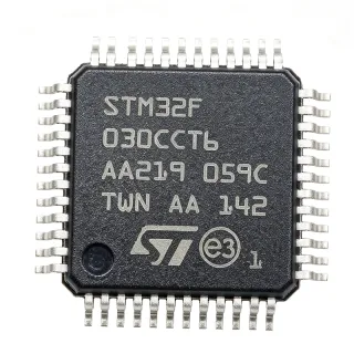
LPC1343FBD48,151 - 32KB Flash 72MHz Cortex-M3 MCU | NXP
MPN: LPC1343FBD48,151 ✓ Active| Qty | Unit Price | Extended |
|---|---|---|
| 1 | $7.16 | $7.16 |
| 10 | $6.45 | $64.50 |
| 100 | $5.72 | $572.00 |
| 500 | $5.1 | $2,550.00 |
| 1,000 | $4.62 | $4,620.00 |
LPC1343FBD48,151 Overview
An ARM Cortex-M3 microcontroller is a 32-bit RISC processor core designed by Arm Holdings for low-power, deterministic embedded use. It belongs to the Cortex-M family of microcontrollers, which are derived from the ARMv7-M architecture and feature a Thumb-2 instruction set, hardware single-cycle multiply, and a Nested Vectored Interrupt Controller (NVIC). Cortex-M3 sits below Cortex-M4 in the hierarchy (no DSP extensions, no FPU) but above Cortex-M0/M0+ in performance and instruction density. Within NXP's portfolio, the LPC1300 family is the lowest-tier Cortex-M3 line, intended as a cost-down replacement for LPC1100 Cortex-M0 designs and as a stepping stone to the LPC1500 Cortex-M3 family.
Key features include 32KB on-chip Flash, 8KB SRAM, a 72MHz maximum CPU clock with a 3-stage Harvard pipeline, USB 2.0 full-speed device with on-chip PHY, a 10-bit ADC with 8 channels and conversion rates up to 400 ksps, two SSP/SPI controllers, one I2C-bus interface, one Fast-mode Plus I2C, a UART, and four general-purpose counter/timers. The device also includes a windowed Watchdog Timer, a 12 MHz internal RC oscillator trimming to 1% accuracy, and support for four low-power modes (Sleep, Deep-sleep, Power-down, and Deep-Down) that draw as little as a few microamps.
Architecturally, the LPC1343 combines the Cortex-M3 core with an AHB-Lite bus matrix, a dedicated ROM-based boot loader with USB MSC/HID drivers, and a unique configuration word (CONFIG) that lets designers fine-tune oscillator trimming and Flash erase behavior. The integrated USB PHY eliminates the need for external 48 MHz crystals on most designs, and the built-in HID/Mass Storage boot loader enables in-field firmware upgrades without a JTAG programmer.
Typical applications include USB peripherals (HID keyboards, mice, CDC serial bridges), low-cost sensor hubs, building automation nodes, point-of-sale terminals, and battery-powered embedded devices where low active current (~10 mA at 72 MHz) and deep-sleep current (~1 uA) are critical.
Design consideration: enable the on-chip pull-up resistor on the VBUS pin to detect USB insertion without external components, and ensure the ISP entry pin (PIO0_1) is held low at reset only when you intend to enter In-System Programming mode, since accidental low on this pin at power-up halts user code execution.
This page synthesizes distributor pricing for the ",151" tray variant, drop-in package alternatives, and practical design notes not found in the standalone manufacturer datasheet.
Drop-in alternatives for LPC1343FBD48,151 — same package, pin-to-pin compatible. Different-package parts requiring PCB rework are excluded.
Variants in this series
Same-series models that are drop-in compatible with LPC1343FBD48,151 (same form factor and footprint) — differing in Package, USB, Mounting Type, Core, ADC.
Quick Comparison Tool — Select alternative parts for side-by-side comparison:
LPC1343FBD48,151
✅ Drop-In✓ In Stock
$4.62 / Unit
View Datasheet →LPC1343FBD48,157
✅ Drop-In📋 Reference alternative (not in catalog)
LPC1342FBD48,151
✅ Drop-In✓ In Stock
$1.54 / Unit
View Datasheet →LPC1343FBD48,151
✅ Drop-In✓ In Stock
$4.62 / Unit
View Datasheet →STM32F072C8T6
✅ Drop-In✓ In Stock
$5.4354 / Unit
View Datasheet →PIC32MX250F128B-I/SP
✅ Drop-In✓ In Stock
$4.31 / Unit
View Datasheet →LPC1343FBD48,151 Maximum Ratings & Electrical Characteristics
| Core | ARM Cortex-M3 |
| Architecture | 32-bit RISC (ARMv7-M, Thumb-2) |
| Maximum CPU Frequency | 72 MHz |
| Pipeline Stages | 3-stage Harvard |
| Program Flash | 32 KB |
| SRAM | 8 KB |
| ROM Boot Loader | Yes (USB MSC/HID drivers) |
| Supply Voltage (VDD) | 2.0 V to 3.6 V |
| USB Controller | USB 2.0 Full-Speed Device with on-chip PHY |
| ADC | 10-bit, 8 channels, up to 400 ksps |
| SSP/SPI Controllers | 2 |
| I2C Interfaces | 1 standard + 1 Fast-mode Plus |
| UART | 1 |
| General-Purpose Timers | 4 |
| Watchdog Timer | Windowed WDT |
| Internal RC Oscillator | 12 MHz, 1% accuracy after trim |
| GPIO Pins | 40 (approx.) |
| Low-Power Modes | Sleep, Deep-sleep, Power-down, Deep-down |
| Operating Temperature | -40 C to +85 C |
| Package | LQFP-48 (7x7 mm) |
| Mounting Type | Surface Mount |
| RoHS Status | Compliant |
| Lead-Free | Yes |
| Packaging | Tray (suffix ,151) |
LPC1343FBD48,151 Pin Configuration
| Pin 1 | PIO0_22/AD7 — GPIO / ADC input 7 |
| Pin 2 | PIO0_23/AD8 — GPIO / ADC input 8 (note: package is 48-pin, only some AD channels exposed) |
| Pin 3 | VBUS — USB VBUS sensing input (5 V tolerant) |
| Pin 4 | VDD — 3.3 V supply voltage |
| Pin 5 | VSS — Ground |
| Pin 6 | PIO0_21/AD6 — GPIO / ADC input 6 |
| Pin 7 | PIO0_20/AD5 — GPIO / ADC input 5 |
| Pin 8 | PIO1_19 — GPIO |
| Pin 9 | PIO1_20 — GPIO |
| Pin 10 | PIO1_21 — GPIO |
| Pin 11 | PIO1_22 — GPIO |
| Pin 12 | PIO1_23 — GPIO |
| Pin 13 | PIO0_19 — GPIO |
| Pin 14 | PIO0_18 — GPIO |
| Pin 15 | PIO0_17 — GPIO / SSP0 CLK (alt function) |
| Pin 16 | VDD — 3.3 V supply voltage |
| Pin 17 | VSS — Ground |
| Pin 18 | PIO1_31 — GPIO / ISP entry pin on reset |
| Pin 19 | PIO1_30 — GPIO |
| Pin 20 | PIO0_16 — GPIO |
| Pin 21 | PIO1_29 — GPIO |
| Pin 22 | PIO0_15 — GPIO |
| Pin 23 | XTAL1 — Crystal oscillator input (12 MHz typical) |
| Pin 24 | XTAL2 — Crystal oscillator output |
| Pin 25 | RESET — Active-low reset input (open-drain) |
| Pin 26 | VDDA — Analog 3.3 V supply (for ADC/PLL) |
| Pin 27 | VSSA — Analog ground |
| Pin 28 | AD0/PIO0_11 — ADC input 0 / GPIO |
| Pin 29 | AD1/PIO1_0 — ADC input 1 / GPIO |
| Pin 30 | AD2/PIO1_1 — ADC input 2 / GPIO |
| Pin 31 | AD3/PIO1_2 — ADC input 3 / GPIO |
| Pin 32 | AD4/PIO1_3 — ADC input 4 / GPIO |
| Pin 33 | VSS — Ground |
| Pin 34 | PIO0_10 — GPIO / I2C SDA |
| Pin 35 | PIO0_11 — GPIO / I2C SCL (alt function mapping per datasheet) |
| Pin 36 | USB_DP — USB D+ data line |
| Pin 37 | USB_DM — USB D- data line |
| Pin 38 | VDD — 3.3 V supply voltage |
| Pin 39 | PIO0_9 — GPIO / SSP0 MISO |
| Pin 40 | PIO0_8 — GPIO / SSP0 MOSI |
| Pin 41 | PIO0_7 — GPIO / SSP0 SSEL / CTS |
| Pin 42 | PIO0_6 — GPIO / SSP0 SCK |
| Pin 43 | PIO0_5 — GPIO |
| Pin 44 | PIO0_4 — GPIO |
| Pin 45 | PIO0_3 — GPIO / UART0 TXD |
| Pin 46 | PIO0_2 — GPIO / UART0 RXD |
| Pin 47 | PIO0_1 — GPIO / ISP entry pin (PIO0_1 low at reset enters ISP mode) |
| Pin 48 | PIO0_0 — GPIO |
Typical Applications
LPC1343FBD48,151 is suitable for 6 applications: USB HID Keyboard / Mouse, Industrial Sensor Hub, Building Automation Controller, Point-of-Sale (POS) Terminal, Battery-Powered Wearable Device, USB-to-UART Bridge / CDC Device.
USB HID Keyboard / Mouse
The LPC1343FBD48,151 fits USB Human Interface Device designs because its on-chip USB 2.0 full-speed PHY eliminates the external transceiver and the ROM-resident HID boot loader enables drag-and-drop firmware updates. The 72 MHz Cortex-M3 core provides more than enough headroom for HID report generation at the 1 kHz USB polling rate, and the 32 KB Flash comfortably fits typical HID descriptors, matrix-scan logic, and anti-ghosting code. The device's low deep-sleep current (a few microamps in Deep-down mode) is a key benefit for wireless or battery-powered peripherals. Place the part on the main board with a 12 MHz crystal reference, route USB D+/D- as a 90-ohm differential pair, and tie VBUS to a 5 V-tolerant pin for host detection.
Recommended
Industrial Sensor Hub
For industrial sensor aggregation nodes, the LPC1343FBD48,151 integrates an 8-channel 10-bit ADC that can scan multiple analog sensors (temperature, pressure, current) at up to 400 ksps, plus two SSP/SPI ports for digital sensors and an I2C Fast-mode Plus bus for higher-speed peripherals. The 72 MHz Cortex-M3 handles filter computation and Modbus RTU framing on the UART, while the 8 KB SRAM is sufficient for 32-point moving-average buffers. Industrial sensors typically need -40 C to +85 C operation, which the LPC1343 supports. For robust communication, add an RS-485 transceiver such as MAX3485 on the UART pins and isolate the bus with an ADuM1411 digital isolator.
Recommended
Building Automation Controller
The LPC1343FBD48,151 is well suited to building-automation controllers (HVAC, lighting, blind/shade control) because of its low power, integrated USB for commissioning laptops, and multiple communication interfaces. The two SSP/SPI controllers can drive addressable LED strips and digital potentiometers, while the I2C bus can connect to environmental sensors (temperature, humidity, CO2) and to a host-touch controller. Active current of ~10 mA at 72 MHz means it can be continuously powered from a small 3.3 V LDO; deep-sleep mode drops to microamps for energy-harvested nodes. The Cortex-M3 core can run a lightweight BACnet/Modbus stack at real-time deadlines.
Recommended
Point-of-Sale (POS) Terminal
In a point-of-sale terminal, the LPC1343FBD48,151 handles keypad scanning, LCD driving, magnetic-stripe reader interfacing, and USB connection to a host PC for transaction forwarding. The integrated USB device controller lets the terminal enumerate as a HID keyboard or CDC virtual COM port without external components. The 32 KB Flash accommodates the keypad mapping table, mag-stripe decode routines, and USB descriptor stack, while 8 KB SRAM provides frame buffers for small graphical LCDs. The 72 MHz core can sustain 50 transactions per second, well above retail POS throughput requirements. Add an external mag-stripe head amplifier (e.g., MagTek 21040101) and a 2x16 character LCD for a complete terminal design.
Recommended
Battery-Powered Wearable Device
The LPC1343FBD48,151 fits wearable designs that occasionally connect to USB for charging or data sync, where the on-chip USB PHY eliminates the need for a separate charging controller's USB interface. Its Deep-down power-down mode consumes only a few microamps, allowing months of standby on a small Li-ion cell. The Cortex-M3 at 72 MHz can drive a low-power OLED display at 30 fps while still drawing under 10 mA active. The 32 KB Flash accommodates Bluetooth Low Energy stack stubs or proprietary RF protocols when paired with an external transceiver. For charging, use a dedicated Li-ion charger IC like MCP73831 and route VBUS to the USB PHY pin.
Recommended
USB-to-UART Bridge / CDC Device
For legacy serial equipment modernization, the LPC1343FBD48,151 is an ideal USB-to-UART bridge because the on-chip USB CDC class support in the ROM bootloader exposes a virtual COM port without any user firmware, and the UART peripheral can be wired to RS-232/RS-485 transceivers for legacy peripherals. The 32 KB Flash supports protocol converters (USB-CDC to Modbus RTU or USB-CDC to I2C bridge), and the 72 MHz core can sustain full-duplex UART throughput at 921600 baud. Common use cases include industrial machines, scientific instruments, and development-board debug ports. Add a MAX3232 for true RS-232 levels or an FTDI-style header for TTL.
Recommended
Recommended Products Summary
Engineering reference data for LPC1343FBD48,151 — comparison, design guidance, and compliance information.
Selection Guide
Comparison with Alternatives
| Parameter | This Product | LPC1343FBD48,157 | LPC1342FBD48,151 | STM32F072C8T6 | PIC32MX250F128B-I/SP |
|---|---|---|---|---|---|
| Brand | NXP Semiconductors | NXP Semiconductors | NXP Semiconductors | STMicroelectronics | Microchip Technology |
| Package | LQFP-48 (7x7 mm) | LQFP-48 (7x7 mm) - same | LQFP-48 (7x7 mm) - same | LQFP-48 (7x7 mm) - same | LQFP-48 - same |
| Core | ARM Cortex-M3 | ARM Cortex-M3 | ARM Cortex-M3 | ARM Cortex-M0 | MIPS M4K |
| Maximum Clock | 72 MHz | 72 MHz | 72 MHz | 48 MHz | 50 MHz |
| Program Flash | 32 KB | 32 KB | 16 KB (-50%) | 64 KB (+100%) | 128 KB (+300%) |
| SRAM | 8 KB | 8 KB | 8 KB | 16 KB (+100%) | 32 KB (+300%) |
| USB | USB 2.0 FS Device + on-chip PHY | USB 2.0 FS Device + on-chip PHY | USB 2.0 FS Device + on-chip PHY | USB 2.0 FS Device + on-chip PHY | USB 2.0 FS Device + on-chip PHY |
| ADC | 10-bit, 8 channels | 10-bit, 8 channels | 10-bit, 8 channels | 12-bit, 10 channels | 10-bit, 9 channels |
| Supply Voltage | 2.0 V to 3.6 V | 2.0 V to 3.6 V | 2.0 V to 3.6 V | 2.0 V to 3.6 V | 2.3 V to 3.6 V |
| Operating Temperature | -40 C to +85 C | -40 C to +85 C | -40 C to +85 C | -40 C to +85 C | -40 C to +85 C |
Key Differentiators
- Integrated USB 2.0 full-speed PHY with ROM bootloader (vs STM32F072C8T6)
- Larger Flash than LPC1342FBD48,151 (vs LPC1342FBD48,151)
- Cortex-M3 core vs Cortex-M0 / MIPS M4K (vs STM32F072C8T6, PIC32MX250F128B-I/SP)
- Tray packaging for prototyping (vs LPC1343FBD48,157)
Design Notes
The LPC1343FBD48,151 has four power pins (VDD) and four ground pins (VSS) that must each be decoupled with a 100 nF ceramic capacitor placed within 5 mm of the pin. The VDDA pin additionally requires a 100 nF + 10 uF decoupling pair because it supplies the ADC and PLL; using a ferrite bead to isolate VDDA from VDD improves ADC noise performance by 5-10 LSB. Estimated: at 72 MHz active current ~10 mA, a 100 nF cap has ~3 mV droop during a clock edge burst - within spec.
The PIO0_1 pin serves double duty as the ISP (In-System Programming) entry pin: if it is held LOW at reset, the chip enters USB-MSC bootloader mode instead of running user code. Common pitfalls include leaving a low-going reset button on PIO0_1 unguarded, or designing the ISP button as a pull-up to VDD with an active-low button to GND (correct). Always add a 10 kohm pull-up on PIO0_1 and route the ISP button so the line is high during normal power-up.
Route USB D+ (pin 36) and USB- (pin 37) as a 90-ohm differential pair on the top layer, keep the pair length-matched within 2 mm, and place a 27 pF to 33 pF series resistor network or ferrite bead for EMI suppression as recommended in UM10375. Avoid routing the USB pair adjacent to clock traces or switching regulator inductors to minimize EMI and radiated emissions. The VBUS pin (pin 3) should be tied through a divider to the USB_VBUS sensing logic.
The LPC1343FBD48,151 is rated for industrial -40 C to +85 C operation. Estimated: at full activity (72 MHz, all peripherals clocked) the device dissipates ~33 mW, well below the LQFP-48 thermal limit of ~500 mW. For enclosed industrial designs without airflow, derate the ambient by 5 C to provide margin. The exposed thermal pad on the LQFP-48 is not present; thermal dissipation is via the standard gull-wing leads.
The 12 MHz crystal on XTAL1/XTAL2 (pins 23 and 24) should be a fundamental-mode crystal with an ESR of less than 60 ohms and a load capacitance matching the crystal specification (typically 10-20 pF). Place the crystal within 5 mm of the MCU, guard the traces with a ground ring, and keep high-frequency digital signals (SSP, UART) away from XTAL traces. For USB operation without an external crystal, the internal 12 MHz RC oscillator trimmed to 1% accuracy is acceptable per USB 2.0 spec.
Compliance Information
RoHS compliant per NXP product page. Lead-free finish. Not AEC-Q100 qualified - this is an industrial-grade part. For automotive applications, NXP offers LPC1343FBD48,151 Q-version (AEC-Q100 qualified).