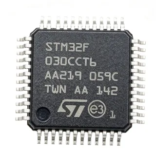
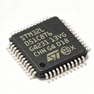
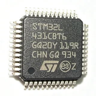
LPC1517JBD48 - Cortex-M3 MCU, 72MHz, 128KB Flash, USB, CAN | NXP
MPN: LPC1517JBD48 ✓ Active| Qty | Unit Price | Extended |
|---|---|---|
| 1 | $6.95 | $6.95 |
| 10 | $6.21 | $62.10 |
| 100 | $5.48 | $548.00 |
| 500 | $4.92 | $2,460.00 |
| 1,000 | $4.35 | $4,350.00 |
LPC1517JBD48 Overview
An ARM Cortex-M3 microcontroller belongs to the Cortex-M family of processors optimized for deterministic, low-power embedded workloads. The Cortex-M3 core combines a 3-stage pipeline, Thumb-2 instruction set, and NVIC (Nested Vectored Interrupt Controller) for low-latency interrupt response. The LPC15xx family extends this foundation with motor-control-oriented peripherals including PWM, QEI (Quadrature Encoder Interface), and dual-sample-and-hold ADCs - making it ideal for field-oriented control (FOC) of brushless DC and permanent-magnet synchronous motors.
Key features include dedicated motor-control PWM with center-aligned mode, two 12-bit successive-approximation ADCs capable of simultaneous dual-channel sampling, a hardware QEI for position feedback, and an integrated temperature sensor. Additional peripherals include 3 USART, 2 SPI, 2 I2C, USB FS device with on-chip PHY, RTC, and a windowed watchdog timer. The LQFP-48 footprint exposes up to 38 GPIO lines with interrupt capability on every pin.
The LPC1500 series incorporates a high-precision analog front end featuring 2/2 MSPS dual-sample-and-hold ADCs and a 10-bit DAC for reference generation. The Cortex-M3 core includes a memory protection unit (MPU) and a wake-up interrupt controller for low-power sleep modes. The device operates from a 2.4V to 3.6V supply.
Typical applications include sensorless BLDC motor drives (fans, pumps, E-bikes), field-oriented control of PMSM motors in industrial servo drives, robotic actuators and CNC auxiliary axes, automotive HVAC and cooling subsystems, and factory automation motion controllers. The dual ADC and hardware QEI are specifically architected for the simultaneous control of two motors, enabling multi-axis drives in highly flexible configurations.
When designing with this MCU, allocate adequate decoupling near the VDDA/VREGB supply pins and provide a low-impedance ground pour under the LQFP-48 package. For motor-control applications, ensure the high-current gate-driver ground returns are isolated from the analog ground plane to prevent ADC reference noise from corrupting current-sense measurements.
This page synthesizes distributor pricing, drop-in same-package alternatives from the LPC15xx family, and practical design considerations that are not consolidated in the manufacturer datasheet.
Drop-in alternatives for LPC1517JBD48 — same package, pin-to-pin compatible. Different-package parts requiring PCB rework are excluded.
Quick Comparison Tool — Select alternative parts for side-by-side comparison:
LPC1518JBD48
✅ Drop-In ⚠️ Specs Unverified📋 Reference alternative (not in catalog)
LPC1548JBD48
✅ Drop-In ⚠️ Specs Unverified📋 Reference alternative (not in catalog)
LPC1519JBD48
✅ Drop-In ⚠️ Specs Unverified📋 Reference alternative (not in catalog)
LPC1517JBD48E
✅ Drop-In📋 Reference alternative (not in catalog)
LPC1549JBD48
✅ Drop-In ⚠️ Specs Unverified📋 Reference alternative (not in catalog)
LPC1517JBD48 Maximum Ratings & Electrical Characteristics
| Core Architecture | ARM Cortex-M3 |
| Maximum CPU Frequency | 72 MHz |
| Flash Memory | 128 kB |
| SRAM | 32 kB |
| Operating Voltage | 2.4 V to 3.6 V |
| ADC | 12-bit, dual sample-and-hold |
| DAC | 10-bit |
| USB | USB 2.0 Full-Speed device with on-chip PHY |
| CAN | 1x CAN 2.0B |
| USART | 3 |
| SPI | 2 |
| I2C | 2 |
| GPIO Count | Up to 38 |
| Package | LQFP-48 (7x7 mm) |
| Mounting Type | Surface Mount |
| Operating Temperature | -40 C to +105 C (industrial) |
| RoHS Status | Compliant |
LPC1517JBD48 Pin Configuration
| Pin 1 | P0_0 — General-purpose digital I/O with interrupt |
| Pin 2 | P0_1 — General-purpose digital I/O |
| Pin 3 | P0_2 — General-purpose digital I/O |
| Pin 4 | P0_3 — General-purpose digital I/O |
| Pin 5 | VDD — 3.3V core supply |
| Pin 6 | VSS — Ground |
| Pin 7 | P1_0 — Digital I/O / ADC0 channel 0 |
| Pin 8 | P1_1 — Digital I/O / ADC0 channel 1 |
| Pin 9 | P1_2 — Digital I/O / ADC0 channel 2 |
| Pin 10 | P1_3 — Digital I/O / ADC0 channel 3 |
| Pin 11 | P1_4 — Digital I/O / ADC0 channel 4 |
| Pin 12 | P1_5 — Digital I/O / ADC0 channel 5 |
| Pin 13 | P1_6 — Digital I/O / ADC0 channel 6 |
| Pin 14 | P1_7 — Digital I/O / ADC0 channel 7 |
| Pin 15 | VDDA — Analog 3.3V supply |
| Pin 16 | VSSA — Analog ground |
| Pin 17 | P2_0 — Digital I/O / ADC1 channel 0 / DAC output |
| Pin 18 | P2_1 — Digital I/O / ADC1 channel 1 |
| Pin 19 | P2_2 — Digital I/O / ADC1 channel 2 |
| Pin 20 | P2_3 — Digital I/O / ADC1 channel 3 |
| Pin 21 | P2_4 — Digital I/O / ADC1 channel 4 |
| Pin 22 | P2_5 — Digital I/O / ADC1 channel 5 |
| Pin 23 | P2_6 — Digital I/O / ADC1 channel 6 |
| Pin 24 | P2_7 — Digital I/O / ADC1 channel 7 |
| Pin 25 | P3_0 — Digital I/O / PWM output |
| Pin 26 | P3_1 — Digital I/O / PWM output |
| Pin 27 | P3_2 — Digital I/O / QEI phase A |
| Pin 28 | P3_3 — Digital I/O / QEI phase B |
| Pin 29 | P3_4 — Digital I/O / QEI index |
| Pin 30 | P3_5 — Digital I/O / USB DP |
| Pin 31 | P3_6 — Digital I/O / USB DM |
| Pin 32 | P3_7 — Digital I/O / CAN RD |
| Pin 33 | P4_0 — Digital I/O / CAN TD |
| Pin 34 | P4_1 — Digital I/O / I2C0 SCL |
| Pin 35 | P4_2 — Digital I/O / I2C0 SDA |
| Pin 36 | P4_3 — Digital I/O / SPI0 SCK |
| Pin 37 | P4_4 — Digital I/O / SPI0 MOSI |
| Pin 38 | P4_5 — Digital I/O / SPI0 MISO |
| Pin 39 | P4_6 — Digital I/O / U0_TXD |
| Pin 40 | P4_7 — Digital I/O / U0_RXD |
| Pin 41 | P5_0 — Digital I/O / U1_TXD |
| Pin 42 | P5_1 — Digital I/O / U1_RXD |
| Pin 43 | XTALIN — Crystal oscillator input |
| Pin 44 | XTALOUT — Crystal oscillator output |
| Pin 45 | RST — Reset (active low) |
| Pin 46 | VBAT — RTC battery supply |
| Pin 47 | VREF — ADC voltage reference |
| Pin 48 | VSS — Ground |
Typical Applications
LPC1517JBD48 is suitable for 6 applications: Sensorless BLDC Motor Drive, Industrial Servo Drive, Automotive HVAC and Cooling Fans, Factory Automation Motion Controller, Robotic Actuator / Drone ESC, Medical Infusion Pump / Diagnostic Device.
Sensorless BLDC Motor Drive
The LPC1517JBD48 is purpose-built for sensorless BLDC motor drives used in fans, pumps, and E-bike traction systems. Its dual 12-bit sample-and-hold ADC enables simultaneous phase-current sensing in a field-oriented control (FOC) loop, with up to 2 MSPS per channel. The 72 MHz Cortex-M3 core executes one FOC iteration in roughly 5 microseconds, leaving ample headroom for housekeeping tasks. On-chip QEI supports sensored fallback when back-EMF is unreliable at low RPM. Integrated CAN 2.0B enables CANopen and DeviceNet integration for industrial servo networks.
Recommended
Industrial Servo Drive
The LPC1517JBD48 is well suited to industrial servo drives controlling PMSM motors in CNC auxiliary axes, robotic joints, and AGV wheel modules. Its PWM timer supports center-aligned mode with hardware dead-time insertion up to 50 nanoseconds, eliminating shoot-through faults in the half-bridge. The hardware Quadrature Encoder Interface (QEI) reads incremental encoders up to 24 MHz with index pulse for homing. USB FS device permits field firmware updates via service laptop. The 2.4V-3.6V supply range and -40 to +105 C operation suit harsh factory-floor environments.
Recommended
Automotive HVAC and Cooling Fans
The LPC1517JBD48 targets automotive HVAC blowers, radiator cooling fans, and oil-pump drives. Its dual ADC samples two phase currents simultaneously to compute rotor position, while the PWM generates complementary outputs up to 100 kHz with programmable dead-time. On-chip CAN supports seamless integration with the vehicle bus for torque/speed commands. The 32 kB SRAM accommodates small RTOS kernels or state-machine firmware. Although not AEC-Q100 qualified, designers can qualify it via NXP's PCN history for non-safety HVAC subsystems.
Recommended
Factory Automation Motion Controller
The LPC1517JBD48 serves as a peripheral motion controller in factory-automation PLCs, handling stepper or BLDC axes under a central PLC's command. Its USB FS device and CAN 2.0B interfaces connect to industrial networks (CANopen, Modbus, USB-CDC) for configuration and diagnostics. The 10-bit DAC provides analog reference voltages to legacy servo amplifiers. The 128 kB flash stores motion profiles and PID tuning tables, while 32 kB SRAM buffers trajectory commands. RTC and watchdog support deterministic, fail-safe operation in unattended cabinets.
Recommended
Robotic Actuator / Drone ESC
The LPC1517JBD48 is suited for small robotic actuators and drone electronic speed controllers (ESCs) that require fast FOC loops in a compact LQFP-48 footprint. The 72 MHz Cortex-M3 with hardware single-cycle MAC completes one FOC iteration in 5 microseconds, supporting 8 kHz update rates typical of mini-quadcopter ESCs. The 12-bit ADC with 2 MSPS sampling captures high-bandwidth current signals from drone motors. On-chip USB allows in-field tuning via a Betaflight-style configurator, while the LQFP-48 footprint is small enough for 20x20 mm ESC boards.
Recommended
Medical Infusion Pump / Diagnostic Device
The LPC1517JBD48 supports medical infusion pumps and diagnostic instruments that need a deterministic Cortex-M3 core and rich analog peripherals in a small LQFP-48 package. The 12-bit dual ADC simultaneously samples flow-rate and pressure sensors for closed-loop delivery control. USB FS device enables host-software logging and calibration. The Cortex-M3 MPU enables isolation of safety-critical firmware from non-safety tasks. While not FDA-listed, the LPC15xx family has been used in IEC 62304-compliant Class B medical firmware per NXP safety manuals.
Recommended
Recommended Products Summary
Engineering reference data for LPC1517JBD48 — comparison, design guidance, and compliance information.
Selection Guide
Comparison with Alternatives
| Parameter | This Product | LPC1518JBD48 | LPC1548JBD48 | LPC1519JBD48 | LPC1517JBD48E | LPC1549JBD48 |
|---|---|---|---|---|---|---|
| Package | LQFP-48 (7x7) | LQFP-48 (7x7) - same | LQFP-48 (7x7) - same | LQFP-48 (7x7) - same | LQFP-48 (7x7) - same | LQFP-48 (7x7) - same |
| Brand | NXP Semiconductors | NXP Semiconductors | NXP Semiconductors | NXP Semiconductors | NXP Semiconductors | NXP Semiconductors |
| Flash Memory | 128 kB | 256 kB | 256 kB | 256 kB | 128 kB | 256 kB |
| SRAM | 32 kB | 32 kB | 36 kB | 36 kB | 32 kB | 36 kB |
| CPU Core | ARM Cortex-M3 @ 72 MHz | ARM Cortex-M3 @ 72 MHz | ARM Cortex-M3 @ 72 MHz | ARM Cortex-M3 @ 72 MHz | ARM Cortex-M3 @ 72 MHz | ARM Cortex-M3 @ 72 MHz |
| USB | FS device | FS device | FS device | FS device | FS device | FS Host/Device/OTG |
| CAN | 1x CAN 2.0B | 1x CAN 2.0B | 2x CAN 2.0B | 2x CAN 2.0B | 1x CAN 2.0B | 2x CAN 2.0B |
| ADC | 12-bit dual sample-and-hold | 12-bit dual sample-and-hold | 12-bit dual sample-and-hold | 12-bit dual sample-and-hold | 12-bit dual sample-and-hold | 12-bit dual sample-and-hold |
| GPIO Count | Up to 38 | Up to 38 | Up to 38 | Up to 38 | Up to 38 | Up to 38 |
| Operating Temperature | -40 C to +105 C | -40 C to +105 C | -40 C to +105 C | -40 C to +105 C | -40 C to +105 C | -40 C to +105 C |
Key Differentiators
- Dual sample-and-hold ADC with hardware trigger (vs LPC1518JBD48 (same peripheral set))
- Hardware QEI for incremental encoders (vs Generic Cortex-M3 MCUs without QEI (e.g., STM32F030C8T6 in LQFP-48))
- On-chip USB FS PHY (vs MCUs requiring external USB PHY)
- Cost-optimized 128 kB flash for code-constrained designs (vs LPC1548JBD48 (256 kB flash, same package))
Design Notes
Decouple VDD, VDDA and VBAT independently with 100 nF X7R ceramic capacitors placed within 3 mm of the respective pins. Estimated: at 72 MHz Cortex-M3 full load the LPC1517JBD48 draws approximately 50 mA from VDD; adding a 4.7 uF bulk capacitor near the regulator improves transient response during USB enumeration spikes. The VDDA rail should be powered from a ferrite bead-isolated LDO to prevent switching-noise injection from the digital VDD supply from corrupting ADC readings.
The LQFP-48 package has a theta_JA of approximately 75 C/W on a 4-layer JEDEC test board. Estimated: at typical motor-control workload (CPU 50% active, peripherals active), the LPC1517JBD48 dissipates about 250 mW, giving a junction-to-ambient temperature rise of roughly 19 C above ambient. For closed enclosures, ensure adequate copper pour on top and bottom layers connected to the central thermal pad area. Industrial-grade parts are rated to +105 C ambient, leaving adequate margin for most enclosed installations.
Route the USB DP/DM differential pair with 90-ohm differential impedance and length matching within 150 mils to meet USB 2.0 Full-Speed signal-integrity requirements. Place the 27-ohm series termination resistors near the MCU pins. The CANH/CANL pair also requires 120-ohm characteristic impedance; place a 120-ohm termination resistor at each end of the bus. Keep high-current gate-driver traces away from the analog ADC inputs (P1_0-P2_7) and provide an analog ground island connected to VSSA at a single point.
Do not apply external reset pulses shorter than 1 microsecond - the LPC1517JBD48 internal reset circuit requires at least 1 us of stable logic-low on the RST pin. For crystal selection, keep the load capacitance within 10-20 pF range; higher values cause startup failures. The USB bus-powered mode requires VBUS sensing to be configured in the USBCLK register before enumerating, otherwise enumeration may hang. Always wait for the IRC stabilization bit in the PDRUNCFG register before switching to the PLL.
Estimated: The 12-bit ADC achieves 11.5 ENOB at 1 MSPS with a 50-ohm source impedance; higher source impedances reduce effective resolution due to charge-sharing. Place an external 10 nF buffer capacitor on each ADC input pin used for current sensing. For QEI inputs, route phase A and phase B as a length-matched differential pair (within 50 mils) and place a 1 kohm pull-up if open-drain encoders are used. Avoid routing QEI traces near the PWM outputs to prevent ground-bounce coupling into the index pulse.
Compliance Information
RoHS and REACH compliant per NXP product page. Not AEC-Q100 qualified; for automotive safety applications consider LPC1547JBD64Q1 (AEC-Q100) which uses a different package (LQFP-64).