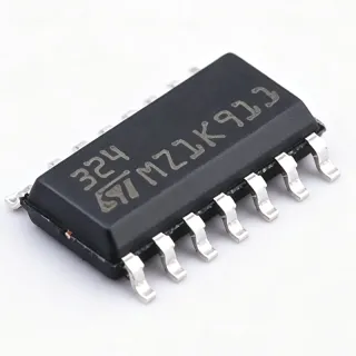
LT6222CDD#PBF - 60MHz Low Power R2R Op Amp | Analog Devices
MPN: LT6222CDD#PBF ✓ Active| Qty | Unit Price | Extended |
|---|---|---|
| 1 | $3.42 | $3.42 |
| 10 | $3.08 | $30.80 |
| 100 | $2.74 | $274.00 |
| 500 | $2.47 | $1,235.00 |
| 1,000 | $2.19 | $2,190.00 |
LT6222CDD#PBF Overview
An operational amplifier (op-amp) is a high-gain voltage amplifier with differential inputs and a single-ended output. It is a fundamental building block in analog electronics, used in signal conditioning, filtering, and amplification. The LT6222CDD#PBF is a rail-to-rail input and output op-amp, meaning its input common-mode range and output swing can reach both supply rails, maximizing dynamic range in low-voltage applications. This makes it suitable for battery-powered and portable devices where headroom is limited.
Key features of the LT6222CDD#PBF include a low supply current of 1mA per amplifier, a low input offset voltage of 100µV (max), and a high open-loop gain of 100dB. The rail-to-rail input and output capability allows it to operate with supply voltages as low as 2.2V, making it ideal for single-supply applications. The device also features a wide bandwidth of 60MHz and a high slew rate of 20V/µs, enabling it to handle fast signals in video and communication systems.
The LT6222CDD#PBF uses a complementary bipolar process technology, which provides excellent DC precision and AC performance. The device is designed for low power consumption without compromising speed, making it suitable for battery-powered instrumentation and portable audio equipment. Its high input impedance and low bias current make it suitable for interfacing with high-impedance sensors.
Typical applications include active filters, data acquisition systems, portable instrumentation, and audio signal conditioning. The quad configuration allows multiple amplifier stages in a single package, saving board space and reducing component count. The rail-to-rail output swing ensures maximum signal amplitude in low-voltage systems.
When designing with the LT6222CDD#PBF, ensure proper power supply decoupling with 0.1µF ceramic capacitors close to the supply pins. The input common-mode range extends to both rails, but for best performance, keep inputs within the specified range. The output can drive capacitive loads up to 100pF without oscillation, but for larger loads, a series resistor may be needed.
Drop-in alternatives for LT6222CDD#PBF — same package, pin-to-pin compatible. Different-package parts requiring PCB rework are excluded.
Quick Comparison Tool — Select alternative parts for side-by-side comparison:
LT6222IDD#PBF
✅ Drop-In ⚠️ Specs Unverified📋 Reference alternative (not in catalog)
LT6222CDD
✅ Drop-In ⚠️ Specs Unverified📋 Reference alternative (not in catalog)
LT6222CDD#TRPBF
✅ Drop-In ⚠️ Specs Unverified📋 Reference alternative (not in catalog)
LT6222CDD#PBF Maximum Ratings & Electrical Characteristics
| Number of Channels | 4 |
| Gain Bandwidth Product | 60 MHz |
| Slew Rate | 20 V/µs |
| Supply Voltage Range | 2.2 V to 12.6 V |
| Supply Current per Amplifier | 1 mA |
| Input Offset Voltage | 100 µV (max) |
| Input Bias Current | 150 nA |
| Rail-to-Rail Input | Yes |
| Rail-to-Rail Output | Yes |
| Open-Loop Gain | 100 dB |
| Input Voltage Noise Density | 12 nV/√Hz |
| Operating Temperature Range | 0°C to 70°C |
| Package | 16-DFN (4x3mm) |
| Mounting Type | Surface Mount |
| RoHS Status | Compliant |
LT6222CDD#PBF Pin Configuration
| Pin 1 | OUT A — Output of amplifier A |
| Pin 2 | IN A- — Inverting input of amplifier A |
| Pin 3 | IN A+ — Non-inverting input of amplifier A |
| Pin 4 | V+ — Positive supply |
| Pin 5 | IN B+ — Non-inverting input of amplifier B |
| Pin 6 | IN B- — Inverting input of amplifier B |
| Pin 7 | OUT B — Output of amplifier B |
| Pin 8 | OUT C — Output of amplifier C |
| Pin 9 | IN C- — Inverting input of amplifier C |
| Pin 10 | IN C+ — Non-inverting input of amplifier C |
| Pin 11 | V- — Negative supply (or ground) |
| Pin 12 | IN D+ — Non-inverting input of amplifier D |
| Pin 13 | IN D- — Inverting input of amplifier D |
| Pin 14 | OUT D — Output of amplifier D |
| Pin 15 | NC — No connect |
| Pin 16 | NC — No connect |
Typical Applications
LT6222CDD#PBF is suitable for 6 applications: Portable Instrumentation, Active Filters, Audio Signal Conditioning, Data Acquisition Systems, Battery-Powered Devices, Video Amplification.
Portable Instrumentation
The LT6222CDD#PBF's low supply current (1mA per amp) and rail-to-rail output make it ideal for battery-powered instruments. Its 60MHz bandwidth ensures accurate signal conditioning for sensors and transducers, while the quad configuration saves board space. The low offset voltage (100µV) maintains measurement precision over temperature.
Recommended
Active Filters
With a gain-bandwidth product of 60MHz, the LT6222CDD#PBF can implement high-frequency active filters for communication and video systems. Its low noise (12nV/√Hz) and high slew rate (20V/µs) preserve signal integrity. The rail-to-rail output allows maximum signal swing in single-supply designs, and the quad package enables multi-stage filters in one IC.
Recommended
Audio Signal Conditioning
The LT6222CDD#PBF is well-suited for audio preamplifiers and equalizers due to its low distortion and high slew rate. Its 60MHz bandwidth ensures minimal phase shift in the audio band, and the low supply current extends battery life in portable audio devices. The quad configuration allows stereo channels with additional filtering stages.
Recommended
Data Acquisition Systems
In data acquisition, the LT6222CDD#PBF provides signal conditioning for analog-to-digital converters. Its low offset voltage and high open-loop gain ensure accurate amplification of small sensor signals. The rail-to-rail input allows direct interface with sensors that output near the supply rails, and the 60MHz bandwidth supports high-speed sampling.
Recommended
Battery-Powered Devices
The LT6222CDD#PBF's low power consumption (1mA per amplifier) is critical for extending battery life in portable devices. Its 2.2V minimum supply voltage allows operation from a single lithium-ion cell. The rail-to-rail output maximizes signal range, and the small DFN package fits compact designs.
Recommended
Video Amplification
With a 60MHz bandwidth and 20V/µs slew rate, the LT6222CDD#PBF can amplify composite video signals with minimal distortion. Its rail-to-rail output provides the required voltage swing for video drivers. The quad configuration allows multiple video channels in one package, reducing component count in multi-camera systems.
Recommended
Recommended Products Summary
Engineering reference data for LT6222CDD#PBF — comparison, design guidance, and compliance information.
Selection Guide
Comparison with Alternatives
| Parameter | This Product | LT6222IDD#PBF | LT6222CDD | AD8608ARUZ |
|---|---|---|---|---|
| Package | 16-DFN (4x3mm) | 16-DFN (4x3mm) | 16-DFN (4x3mm) | 16-TSSOP |
| Brand | Analog Devices | Analog Devices | Analog Devices | Analog Devices |
| Number of Channels | 4 | 4 | 4 | 4 |
| Gain Bandwidth Product | 60 MHz | 60 MHz | 60 MHz | 10 MHz |
| Slew Rate | 20 V/µs | 20 V/µs | 20 V/µs | 5 V/µs |
| Supply Voltage Range | 2.2V to 12.6V | 2.2V to 12.6V | 2.2V to 12.6V | 2.7V to 5.5V |
| Supply Current per Amplifier | 1 mA | 1 mA | 1 mA | 1 mA |
| Input Offset Voltage (max) | 100 µV | 100 µV | 100 µV | 65 µV |
Key Differentiators
- Higher bandwidth than many competing quad op-amps (vs AD8608ARUZ)
- Wider supply voltage range (vs AD8608ARUZ)
- Higher slew rate (vs OPA4340UA)
Design Notes
Ensure proper power supply decoupling by placing 0.1µF ceramic capacitors as close as possible to the V+ and V- pins. For high-frequency applications, add a 10µF tantalum capacitor in parallel to filter low-frequency noise. The LT6222CDD#PBF operates from 2.2V to 12.6V, so verify the supply voltage does not exceed the absolute maximum rating of 13.2V.
For optimal performance, use a ground plane and keep input traces short to minimize parasitic capacitance. The DFN package has an exposed pad on the bottom; solder it to the PCB ground plane for improved thermal dissipation. Follow the recommended PCB layout in the datasheet to reduce stray capacitance and maintain stability.
Avoid driving capacitive loads greater than 100pF directly, as this may cause oscillation. If larger loads are required, add a series resistor (e.g., 50Ω) at the output. Also, ensure the input common-mode voltage stays within the specified range to avoid phase reversal. For single-supply operation, bias the inputs to mid-supply for best performance.
Compliance Information
RoHS compliant per Analog Devices product page. Not AEC-Q100 qualified.