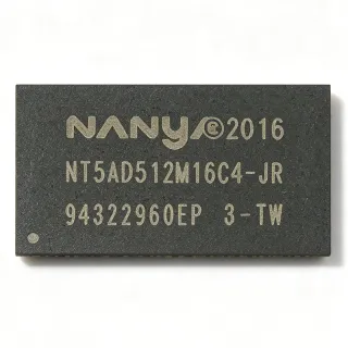
M5M5V108DFP-70H - 1Mbit 128Kx8 70ns Async SRAM | Renesas
MPN: M5M5V108DFP-70H ✗ End of Life| Qty | Unit Price | Extended |
|---|---|---|
| 1 | $5.95 | $5.95 |
| 10 | $5.4 | $54.00 |
| 100 | $4.85 | $485.00 |
| 500 | $4.4 | $2,200.00 |
| 1,000 | $3.95 | $3,950.00 |
M5M5V108DFP-70H Overview
Static RAM is a type of volatile semiconductor memory in which each bit is stored in a flip-flop-style cell, sitting above DRAM in the memory hierarchy where speed and deterministic access matter more than density. Unlike DRAM, SRAM needs no refresh circuitry, making system design simpler and access timing fully predictable for microprocessor bus interfacing.
Key features include fully TTL-compatible inputs and outputs, three-state outputs with OR-tie capability, an output enable (OE) pin that prevents data contention on the I/O bus, common data I/O, and easy memory expansion and power-down control via two chip enables (S1, S2). Data is retained at supply voltages down to +2V, enabling battery-backup schemes. The device is fabricated using high-performance triple-polysilicon and double-metal CMOS technology, with thin-film-transistor (TFT) load cells that reduce standby current.
The -70H speed grade provides 70 ns address access time over a 3V (H) operating voltage range, allowing zero-wait-state or near-zero-wait-state interfacing with mid-range 8/16-bit microcontrollers and legacy embedded CPUs. The 128Kx8 organization maps directly onto byte-wide memory buses, and the DFP 32-pin 525mil SOP footprint supports surface-mount assembly.
Typical applications include legacy embedded systems, industrial control and instrumentation memory expansion, network equipment buffers, telecom line cards, and battery-backed data storage in measurement devices where deterministic asynchronous access is required.
Design consideration: the part is long discontinued by the original manufacturer; new production comes exclusively from authorized aftermarket sources such as Rochester Electronics, so verify lot date codes and include second-source planning in any new design.
This page synthesizes distributor availability, family cross-references, and practical design notes not found in the manufacturer datasheet.
Drop-in alternatives for M5M5V108DFP-70H — same package, pin-to-pin compatible. Different-package parts requiring PCB rework are excluded.
Quick Comparison Tool — Select alternative parts for side-by-side comparison:
M5M5V108DFP-70H#ST
✅ Drop-In📋 Reference alternative (not in catalog)
M5M5V108DFP-55H
✅ Drop-In ⚠️ Specs Unverified📋 Reference alternative (not in catalog)
M5M5V108DFP-85H
✅ Drop-In ⚠️ Specs Unverified📋 Reference alternative (not in catalog)
M5M5V108DFP-70H Specifications
| Memory Type | Asynchronous CMOS Static RAM (SRAM) |
| Memory Size | 1 Mbit (1048576 bit) |
| Organization | 131072 word x 8 bit (128K x 8) |
| Access Time | 70 ns (-70H speed grade) |
| Supply Voltage Range | 3 V class (H version); data retention at +2 V |
| Interface | Parallel, TTL compatible (all inputs and outputs) |
| Output Type | Three-state, common data I/O |
| Chip Enable Control | S1, S2 (memory expansion / power down) |
| Output Enable | Yes (OE prevents I/O bus data contention) |
| Data Retention Voltage | +2 V minimum (battery backup capable) |
| Cell Technology | Triple-polysilicon, double-metal CMOS with TFT load cells |
| Package | 32-pin 525 mil SOP (DFP) |
| Mounting Type | Surface Mount |
| Lifecycle Status | End of Life (aftermarket via Rochester Electronics) |
M5M5V108DFP-70H 32-pin 525 mil sop (dfp) Pin Configuration Guide
Pin configuration for M5M5V108DFP-70H (32-pin 525 mil sop (dfp) package). Pin numbering, functions, and connection diagrams are defined in the manufacturer datasheet. Refer to it for the exact footprint and soldering guidelines.

No detailed pinout data available for M5M5V108DFP-70H.
Refer to the datasheet for full pin configuration.
Typical Applications
M5M5V108DFP-70H is suitable for 6 applications: Legacy Embedded System Memory Expansion, Industrial Instrumentation Data Buffering, Telecom Line Card Memory, Battery-Backed Data Retention Storage, Test and Measurement Equipment, Network Equipment Packet Buffers.
Legacy Embedded System Memory Expansion
The M5M5V108DFP-70H fits legacy embedded controllers that require external byte-wide SRAM with deterministic asynchronous access. Its 128Kx8 organization maps directly to 8-bit data buses with 17 address lines, and the 70 ns access time allows zero-wait-state or one-wait-state operation with common legacy microcontrollers. The dual chip enables S1/S2 simplify bank decoding when expanding to multiple SRAM devices, and TTL-compatible three-state I/O connects directly to the processor bus without external transceivers. Its +2V data retention also supports battery-backed variable storage in systems designed before modern NVRAM alternatives were widespread.
Recommended
Industrial Instrumentation Data Buffering
In industrial measurement and data-logging instruments, the M5M5V108DFP-70H serves as a high-speed scratchpad or log buffer between sensors and non-volatile storage. The asynchronous interface needs no clock, so acquisition timing is deterministic and simple to verify with a scope. The OE pin prevents bus contention during readback, while S1/S2 power-down reduces standby drain between capture sessions. With +2V data retention, buffered records survive brief brown-outs when backed by a small battery supervisor. The 32-pin 525mil SOP package suits the through-hole-era boards common in long-life industrial equipment still being serviced today.
Recommended
Telecom Line Card Memory
Telecom channel cards historically used 128Kx8 SRAM devices like the M5M5V108DFP-70H for per-channel configuration tables and call-state storage. The 70 ns access time supports service of multiple channel interrupts from a shared bus, and three-state OR-tie outputs allow several memory devices to share a common data bus safely thanks to the OE contention-prevention feature. The H-version 3V-class operation matches the reduced-voltage rails used on later line-card designs, and standby power down via S1/S2 limits per-card consumption when channels are idle.
Recommended
Battery-Backed Data Retention Storage
The M5M5V108DFP-70H is well suited to battery-backed storage of calibration constants, counters, and event logs in meters and protective relays. Its datasheet specifies data hold on a +2V supply, so a 3V lithium cell plus a simple supply-switchover circuit retains SRAM contents for years. During normal operation the S1/S2 enables deselect the device into standby automatically; in backup mode the cell drives only retention current, extending battery life compared with parts lacking low-voltage data hold. The 128Kx8 density accommodates substantial parameter tables without external banking logic.
Recommended
Test and Measurement Equipment
Bench instruments such as logic analyzers, curve tracers, and arbitrary waveform generators used asynchronous SRAM like the M5M5V108DFP-70H as acquisition memory and setup storage. The deterministic 70 ns access time simplifies calibration of capture timing across units, and TTL-compatible I/O interfaces cleanly with the 5V/3V logic families found in this equipment class. Field service organizations favor this exact MPN for board-level repair because the SOP footprint can be replaced with hot-air tools, and the Rochester Electronics #ST version provides a legitimate, traceable source of new die for maintenance spares.
Recommended
Network Equipment Packet Buffers
Older routers, switches, and network processors used byte-wide asynchronous SRAM devices such as the M5M5V108DFP-70H for packet descriptor queues and lookup tables. The 70 ns cycle supports line-rate servicing of 10 Mbps-class and early 100 Mbps-class ports, while OR-tie three-state outputs allow multiple SRAM banks on a shared bus with simple OE-based arbitration. Dual chip enables permit direct 128K-word bank pairs without external decoders, shortening PCB routing. Replacement demand remains from service spares stock for equipment still deployed in the field.
Recommended
Recommended Products Summary
Engineering reference data for M5M5V108DFP-70H — comparison, design guidance, and compliance information.
Selection Guide
Comparison with Alternatives
| Parameter | This Product | M5M5V108DFP-70H#ST | M5M5V108DFP-55H | M5M5V108DFP-85H |
|---|---|---|---|---|
| Package | 32-pin 525mil SOP (DFP) | 32-pin 525mil SOP - same | 32-pin 525mil SOP - same | 32-pin 525mil SOP - same |
| Brand | Renesas Electronics (orig. Mitsubishi) | Renesas Electronics (Rochester aftermarket) | Renesas Electronics (orig. Mitsubishi) | Renesas Electronics (orig. Mitsubishi) |
| Memory Organization | 128K x 8 (1 Mbit) | 128K x 8 | 128K x 8 | 128K x 8 |
| Access Time | 70 ns | 70 ns | 55 ns | 85 ns |
| Supply Voltage Class | 3 V (H version) | 3 V (H) | 3 V (H) | 3 V (H) |
| Data Retention | +2 V data hold | +2 V | +2 V | +2 V |
| Lifecycle Status | EOL (broker stock) | Active aftermarket (Rochester) | EOL (broker stock) | EOL (broker stock) |
Key Differentiators
- Authorized aftermarket continuity (vs M5M5V108DFP-70H (original production))
- Faster speed margin (vs M5M5V108DFP-85H)
- Low-voltage data retention (vs M5M5V108DFP-55H)
Design Notes
Use the S1/S2 dual chip enables as an automatic power-down mechanism: hold the device deselected between accesses so it enters standby, minimizing average consumption. For battery-backup designs, the datasheet permits data hold at +2V, so a 3V lithium cell through a supply-mux supervisor retains SRAM contents while nearly all other logic is unpowered. Estimated: retention current draw on battery is typically orders of magnitude below operating current, but confirm the exact standby/retention current figures in the datasheet DC characteristics table for your battery-life calculation.
The 32-pin 525mil SOP footprint is a legacy wide-body package; when reworking these boards, use a hot-air rework profile with preheating because the large SOP body and old FR-4 laminates are prone to pad lifting. Decouple VCC with a 0.1uF ceramic capacitor placed within a few millimeters of the package, as asynchronous SRAM draws short switching-current spikes on each access. Keep address and data lines of similar length when interfacing to 70 ns timing to avoid skewed setup/hold margins at the memory pins.
Do not substitute M5M5V108DVP or DKV package variants for the DFP part on an existing PCB - the electrical die is the same but the land patterns differ. Beware of assuming pin compatibility with generic JEDEC byte-wide SRAMs from other vendors; verify pin-by-pin against the M5M5V108DFP datasheet pinout before drop-in replacement. Finally, all original production is discontinued: source the Rochester Electronics #ST version or verified broker stock, and check date codes on non-authorized inventory to avoid reclaimed or counterfeit devices.
Compliance Information
Legacy Mitsubishi/Renesas part predating modern compliance documentation in available data; Rochester Electronics #ST aftermarket version may carry updated compliance declarations - verify with supplier.