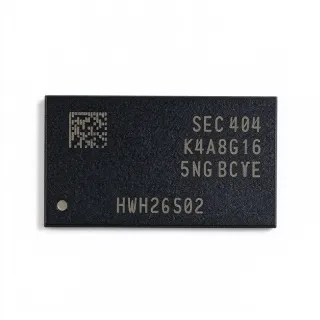
K6F2016U4E-EF70T - 2Mbit Async SRAM 70ns 48-TFBGA | Samsung
MPN: K6F2016U4E-EF70T ✓ Active| Qty | Unit Price | Extended |
|---|---|---|
| 1 | $0 | $0.00 |
| 10 | $0 | $0.00 |
| 100 | $0 | $0.00 |
| 500 | $0 | $0.00 |
| 1,000 | $0 | $0.00 |
K6F2016U4E-EF70T Overview
An asynchronous SRAM is a type of static random-access memory that does not require a clock or refresh cycles: data is accessed whenever address and control signals (CE, OE, WE) are applied, and data is retained as long as power is present. Within the memory-IC hierarchy, it sits under solid-state memory -> RAM -> static RAM -> asynchronous parallel SRAM, complementing DRAM (which needs refresh) and synchronous SRAM (which is clocked). Full-CMOS fabrication gives it very low standby current, making it a natural fit for battery-backed and low-power designs.
Key features of the K6F2016U4E family include the super-low-power full-CMOS process, a wide 2.7V to 3.3V operating supply, industrial operating temperature range support, and a compact 48-ball chip-scale-style package that gives designers board-space flexibility. The 16-bit data bus simplifies interfacing to 16-bit and 32-bit processors without external bus transceivers.
Technically, the device is a parallel asynchronous SRAM: the 70 ns speed grade (tAA) suits mid-speed embedded controllers, and the three control lines (chip enable, output enable, write enable) allow straightforward glueless connection to most microcontrollers and FPGAs. Deep power-down via chip enable keeps standby consumption minimal in portable and battery-backed applications.
Typical applications include battery-powered data acquisition, industrial automation controllers, networking line cards, computer peripherals, and code/data buffering alongside MCUs, FPGAs, and DSPs.
Design consideration: as with all asynchronous SRAMs, respect the address setup, CE pulse width, and data hold timings from the manufacturer datasheet, and use controlled series termination on high-speed address lines to limit ringing.
This page synthesizes distributor availability, drop-in family alternatives, and practical design notes not found in the manufacturer datasheet alone. Pricing shown is request-quote based as of 2026-09-01.
Drop-in alternatives for K6F2016U4E-EF70T — same package, pin-to-pin compatible. Different-package parts requiring PCB rework are excluded.
Variants in this series
Same-series models that are drop-in compatible with K6F2016U4E-EF70T (same form factor and footprint) — differing in Package, Memory Size, Memory Type, Organization, Technology.
Quick Comparison Tool — Select alternative parts for side-by-side comparison:
K6F2016U4E-EF55T
✅ Drop-In ⚠️ Specs Unverified📋 Reference alternative (not in catalog)
K6F2016U4D-FF70T00
✅ Drop-In ⚠️ Specs Unverified✓ In Stock
$2.05 / Unit
View Datasheet →K6F2016U4E-EF55
✅ Drop-In ⚠️ Specs Unverified📋 Reference alternative (not in catalog)
K6F2016U4D-FF55T00
✅ Drop-In ⚠️ Specs Unverified📋 Reference alternative (not in catalog)
K6F2016U4E-EF70T Specifications
| Memory Type | SRAM - Asynchronous |
| Memory Size | 2 Mbit |
| Organization | 128K x 16 |
| Interface | Parallel |
| Access Time (tAA) | 70 ns |
| Supply Voltage (VCC) | 2.7 V to 3.3 V |
| Technology | Full CMOS |
| Package | 48-TFBGA (6 x 7) |
| Mounting Type | Surface Mount |
| Control Signals | CE, OE, WE |
| Refresh Requirement | None (static RAM) |
K6F2016U4E-EF70T 48-tfbga (6 x 7) Pin Configuration Guide
Pin configuration for K6F2016U4E-EF70T (48-tfbga (6 x 7) package). Pin numbering, functions, and connection diagrams are defined in the manufacturer datasheet. Refer to it for the exact footprint and soldering guidelines.

No detailed pinout data available for K6F2016U4E-EF70T.
Refer to the datasheet for full pin configuration.
Typical Applications
K6F2016U4E-EF70T is suitable for 6 applications: Battery-Powered Data Loggers, Industrial Automation Controllers, FPGA Design Buffers and Line Buffers, Networking and Telecom Equipment, Computer Peripherals and Office Equipment, Test and Measurement Instrumentation.
Battery-Powered Data Loggers
The K6F2016U4E-EF70T fits battery-powered data loggers because Samsung characterizes the K6F2016U4E family as a super-low-power, low-voltage full-CMOS static RAM: the full-CMOS cell draws near-zero current when the device is deselected, and no refresh is ever needed, unlike DRAM. In a logger, the 128K x 16 organization provides 256 Kbyte of fast scratch or history storage, and the 2.7V-3.3V supply matches a lithium cell or a 3.3V rail directly, eliminating a regulator stage. The 70 ns access time is far faster than any serial flash, so an MCU can sweep the log buffer quickly and return to sleep. Placed close to the MCU on a short parallel bus with 0.1 uF local decoupling, the SRAM adds negligible energy cost per logged sample, extending battery life in field instruments.
Recommended
Industrial Automation Controllers
Industrial PLC I/O modules and motion controllers use asynchronous SRAM for deterministic, wait-state-free variable storage, and the K6F2016U4E-EF70T suits this role with its 70 ns address access time and industrial temperature range support noted in the Samsung datasheet. The 2 Mbit capacity holds ladder-logic working data, retentive registers, and fault-history buffers, while the 16-bit bus matches the word width of common 16/32-bit controllers without bus packing. Because access is fully asynchronous with simple CE/OE/WE controls, the memory requires no clock domain or FIFO logic, simplifying certification-driven designs. On a control board, keep the address bus under 10 cm where practical and use series termination on data lines to control ringing at backplane speeds; the 48-ball 6 x 7 TFBGA also survives vibration better than leaded packages.
Recommended
FPGA Design Buffers and Line Buffers
The K6F2016U4E-EF70T works well as external buffer memory for FPGAs in image line buffering, network packet staging, and test-instrument capture. A simple HDL memory controller drives the 17-bit address, 16-bit data, and CE/OE/WE signals directly; with a 70 ns tAA, sustained random-access rates around 10-14 MHz are achievable, and sequential bursts can run faster by pipelining address setup. The 2.7V-3.3V IO compatibility lets the SRAM share the FPGA 3.3V bank without level shifters, and the 48-ball TFBGA (6 x 7) footprint consumes under 1 square centimeter of board area. In imaging pipelines, 256 Kbyte stores multiple video lines at VGA width with headroom, and the full-CMOS standby behavior keeps idle power low between capture windows. Match trace lengths on the data bus to minimize skew.
Recommended
Networking and Telecom Equipment
Line cards, switches, and telecom adapters historically use 3.3V asynchronous SRAM for lookup tables, descriptor rings, and queue metadata, and the K6F2016U4E-EF70T provides 2 Mbit of such storage with deterministic 70 ns latency - no refresh pauses and no variable timing. The 128K x 16 organization maps naturally to 16-bit hash entries or status words, and the parallel interface keeps lookup latency constant, which is valuable for packet-path determinism. The 48-ball 6 x 7 TFBGA offers a high board-density footprint for dense line-card layouts, and industrial temperature support covers telecom plant environments. Supply the part from a clean 3.3V rail with 0.1 uF plus 10 uF decoupling at the BGA vias; memory content is normally re-initialized at line-card boot, so battery retention is not required in this application.
Recommended
Computer Peripherals and Office Equipment
Printers, scanners, and point-of-sale peripherals use asynchronous SRAM as a fast working buffer between the main SoC and slower storage, and the K6F2016U4E-EF70T serves this need with its 2 Mbit, 128K x 16 array and 70 ns access. The 2.7V-3.3V supply aligns with the 3.3V peripheral board rails, and the CE/OE/WE control set connects directly to legacy parallel buses still common in printer engines. Distributor listings (Xecor, Chipdigger) explicitly cite computer peripherals and industrial automation as target uses for this part. Because peripheral boards are cost-sensitive, the widely stocked 70 ns grade avoids the premium of faster speeds, and the 6 x 7 mm BGA keeps the memory footprint small on two-layer or four-layer boards. Provide a defined power-on CE pull-up so the bus does not float during reset.
Recommended
Test and Measurement Instrumentation
Bench instruments such as logic analyzers, data acquisition front ends, and function generators use fast SRAM for waveform storage and capture buffers, where the K6F2016U4E-EF70T's fixed 70 ns read latency simplifies real-time control logic compared with SDRAM refresh scheduling. The 16-bit data path stores ADC samples at 12-16 bit resolution without packing overhead, and 2 Mbit yields about 128K samples per channel segment. Industrial temperature support suits rack and bench environments alike, and the low standby current lets battery-powered handheld instruments preserve capture data between measurements. Design the capture controller so the SRAM address bus is driven from a counter for streaming writes and random reads, honoring datasheet CE pulse widths; add ground vias under the BGA to provide a clean return path for the 16-bit switching bus.
Recommended
Recommended Products Summary
Engineering reference data for K6F2016U4E-EF70T — comparison, design guidance, and compliance information.
Selection Guide
Comparison with Alternatives
| Parameter | This Product | K6F2016U4E-EF55T | K6F2016U4D-FF70T00 | K6F2016U4E-EF55 |
|---|---|---|---|---|
| Package | 48-TFBGA (6 x 7) | 48-TFBGA (6 x 7) - same | 48-TFBGA (6 x 7) - same | 48-TFBGA (6 x 7) - same |
| Brand | Samsung | Samsung | Samsung | Samsung |
| Density | 2 Mbit | 2 Mbit | 2 Mbit | 2 Mbit |
| Organization | 128K x 16 | 128K x 16 | 128K x 16 | 128K x 16 |
| Access Time (tAA) | 70 ns | 55 ns | 70 ns class | 55 ns |
| Supply Voltage | 2.7 V to 3.3 V | 2.7 V to 3.3 V | 2.7 V to 3.3 V | 2.7 V to 3.3 V |
| Power Class | Super low power (full CMOS) | Super low power (U4E family) | Low power (U4D family) | Super low power (U4E family) |
| Packing | Tape & Reel (T suffix) | Tape & Reel | Tape & Reel | Tray (non-T suffix) |
Key Differentiators
- Super-low-power full-CMOS standby behavior (vs K6F2016U4D-FF70T00)
- Cost-effective 70 ns speed grade (vs K6F2016U4E-EF55T)
- Board-space efficient 6 x 7 mm BGA (vs K6F2016U4E-EF55)
Design Notes
Place a 0.1 uF ceramic capacitor at each VCC ball pair of the 48-ball TFBGA, within 2 mm of the via fanout, plus one 10 uF bulk capacitor per device. Fan out the BGA with via-in-pad or dog-bone escapes on a four-layer board; dedicate one internal layer as a solid ground plane so the 16-bit data bus has a low-inductance return path. Keep the address and data bus under 10 cm between the SRAM and the controller where practical to bound flight-time skew at moderate bus rates.
At bus cycle times approaching the 70 ns grade, reflections are usually manageable, but still add 22-33 ohm series resistors on data and address lines longer than 8 cm to damp ringing, especially on two-layer boards without an adjacent ground plane. Ensure CE is pulled up (deselected) during controller reset so the SRAM never drives the bus while the FPGA or MCU is tri-stated; bus contention during power-up is a common failure mode in shared-parallel-bus designs.
Ordering-code suffixes on this family carry meaning: EF encodes process/power options, the two digits encode speed grade (55 = 55 ns, 70 = 70 ns), and T indicates Tape & Reel packing. Ordering the non-T suffix delivers trays instead of reels, which affects pick-and-place feeders. Also verify the datasheet timing table for your specific speed grade rather than assuming: write pulse widths and data hold times differ between the 55 ns and 70 ns versions of the K6F2016U4E family.
Compliance Information
Compliance status was not stated in the verified distributor or datasheet excerpts for this legacy Samsung SRAM; request a compliance certificate from the supplier.