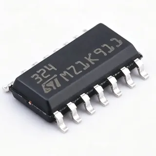
OP42GSZ - High Speed Precision Op Amp | Analog Devices
MPN: OP42GSZ ✓ Active| Qty | Unit Price | Extended |
|---|---|---|
| 1 | $12.68 | $12.68 |
| 10 | $11.5 | $115.00 |
| 100 | $10.2 | $1,020.00 |
| 500 | $9.1 | $4,550.00 |
| 1,000 | $8.25 | $8,250.00 |
OP42GSZ Overview
An operational amplifier (op amp) is a high-gain voltage amplifier with differential inputs and a single-ended output. It is a fundamental building block in analog electronics, used in signal conditioning, filtering, and instrumentation. Op amps are categorized by parameters such as bandwidth, slew rate, input offset voltage, and noise. The OP42GSZ belongs to the precision amplifier family, optimized for accuracy and speed, and is commonly used in data acquisition, test equipment, and audio systems.
Key features of the OP42GSZ include a fast settling time of 800 ns to 0.01%, a wide full-power bandwidth of 900 kHz, and a supply current of less than 6 mA. The JFET input provides high input impedance and low bias current, which is essential for high-impedance sensor interfaces. The device is internally compensated for unity-gain stability, simplifying design.
Technically, the OP42GSZ uses a JFET-input architecture that combines the benefits of low noise and high speed. The symmetric slew rate of 50 V/µs ensures balanced performance for both positive and negative signal transitions. The device is designed to drive capacitive loads without oscillation, making it robust in practical applications.
Typical applications include fast precision integrators, sample-and-hold circuits, and active filters. Its high slew rate and bandwidth make it ideal for video and RF signal processing, while its precision characteristics suit instrumentation and control systems.
When designing with the OP42GSZ, ensure proper power supply decoupling with 0.1 µF ceramic capacitors close to the supply pins. The input common-mode range extends to the negative rail, but for best performance, keep inputs within the specified range. The device is RoHS compliant and available in tape and reel packaging.
Drop-in alternatives for OP42GSZ — same package, pin-to-pin compatible. Different-package parts requiring PCB rework are excluded.
Variants in this series
Same-series models that are drop-in compatible with OP42GSZ (same form factor and footprint) — differing in Package, Slew Rate, Supply Voltage Range.
Quick Comparison Tool — Select alternative parts for side-by-side comparison:
OP42GSZ-REEL7
✅ Drop-In✓ In Stock
$5.4 / Unit
View Datasheet →AD548
✅ Drop-In📋 Reference alternative (not in catalog)
LF357
✅ Drop-In📋 Reference alternative (not in catalog)
TL081
✅ Drop-In📋 Reference alternative (not in catalog)
OP42GSZ Maximum Ratings & Electrical Characteristics
| Amplifier Type | J-FET |
| Number of Circuits | 1 |
| Gain Bandwidth Product | 10 MHz |
| Slew Rate | 50 V/µs |
| Supply Voltage Range | ±8V to ±20V |
| Input Offset Voltage | 5 mV (max) |
| Supply Current | 6 mA (max) |
| Settling Time | 800 ns to 0.01% |
| Full Power Bandwidth | 900 kHz |
| Package | 8-SOIC (0.154, 3.90mm Width) |
| Operating Temperature Range | -40°C to +85°C |
| RoHS | Compliant |
OP42GSZ Pin Configuration
| Pin 1 | OFFSET N1 — Offset null pin 1 |
| Pin 2 | IN- — Inverting input |
| Pin 3 | IN+ — Non-inverting input |
| Pin 4 | V- — Negative supply |
| Pin 5 | OFFSET N2 — Offset null pin 2 |
| Pin 6 | OUT — Output |
| Pin 7 | V+ — Positive supply |
| Pin 8 | NC — No connection |
Typical Applications
OP42GSZ is suitable for 6 applications: Fast Precision Integrators, Sample-and-Hold Circuits, Active Filters, Video Signal Processing, RF Signal Conditioning, Test and Measurement Equipment.
Fast Precision Integrators
The OP42GSZ's high slew rate and fast settling time make it ideal for integrator circuits in analog computing and signal processing. Its 10 MHz bandwidth ensures accurate integration of high-frequency signals, while the JFET input minimizes leakage current, preserving integration accuracy over time. The device's low offset voltage (5 mV max) reduces output error, making it suitable for precision measurement systems.
Recommended
Sample-and-Hold Circuits
In sample-and-hold applications, the OP42GSZ provides fast acquisition and low droop due to its JFET input and high slew rate. The 800 ns settling time to 0.01% ensures accurate capture of fast analog signals, making it suitable for data acquisition systems. The device's high input impedance prevents loading of the source, and its wide supply range allows flexible interface with ADCs.
Recommended
Active Filters
The OP42GSZ is well-suited for active filter designs requiring high bandwidth and fast response. Its 10 MHz gain-bandwidth product allows implementation of filters with cutoff frequencies up to 1 MHz, while the high slew rate prevents distortion in large-signal applications. The JFET input provides low noise and high input impedance, making it ideal for precision filter circuits in instrumentation.
Recommended
Video Signal Processing
With a slew rate of 50 V/µs and a bandwidth of 10 MHz, the OP42GSZ can handle composite video signals with minimal distortion. Its fast settling time ensures accurate reproduction of fast transitions, making it suitable for video buffering and distribution amplifiers. The device's low supply current is beneficial in multi-channel video systems.
Recommended
RF Signal Conditioning
The OP42GSZ's high bandwidth and slew rate make it useful in RF signal conditioning circuits, such as IF amplifiers and AGC loops. Its JFET input provides high input impedance, minimizing loading on RF front-ends. The device's fast settling time is critical for pulsed RF signals, ensuring accurate amplitude measurement.
Recommended
Test and Measurement Equipment
In test and measurement, the OP42GSZ is used in oscilloscope front-ends, waveform generators, and precision voltmeters. Its high slew rate and bandwidth enable accurate reproduction of fast waveforms, while the low offset voltage ensures measurement accuracy. The device's wide supply range allows operation from various power rails in benchtop instruments.
Recommended
Recommended Products Summary
Engineering reference data for OP42GSZ — comparison, design guidance, and compliance information.
Selection Guide
Comparison with Alternatives
| Parameter | This Product | OP42GSZ-REEL7 | OP42GPZ | AD548 | LF357 | TL081 |
|---|---|---|---|---|---|---|
| Package | 8-SOIC | 8-SOIC | 8-PDIP | 8-SOIC | 8-SOIC | 8-SOIC |
| Brand | Analog Devices | Analog Devices | Analog Devices | Analog Devices | Texas Instruments | Texas Instruments |
| Gain Bandwidth Product | 10 MHz | 10 MHz | 10 MHz | 1 MHz | 20 MHz | 3 MHz |
| Slew Rate | 50 V/µs | 50 V/µs | 50 V/µs | 1.8 V/µs | 50 V/µs | 13 V/µs |
| Supply Voltage Range | ±8V to ±20V | ±8V to ±20V | ±8V to ±20V | ±4.5V to ±18V | ±5V to ±18V | ±5V to ±15V |
| Input Offset Voltage | 5 mV (max) | 5 mV (max) | 5 mV (max) | 0.5 mV (max) | 3 mV (max) | 3 mV (max) |
| Supply Current | 6 mA (max) | 6 mA (max) | 6 mA (max) | 0.3 mA (max) | 5 mA (max) | 2.8 mA (max) |
Key Differentiators
- Higher slew rate than AD548 (vs AD548)
- Lower supply current than LF357 (vs LF357)
- Wider supply range than TL081 (vs TL081)
Design Notes
Ensure proper power supply decoupling by placing 0.1 µF ceramic capacitors close to the V+ and V- pins. Additionally, use 10 µF tantalum capacitors at the supply entry points to filter low-frequency noise. This is critical for maintaining the OP42GSZ's high-speed performance and preventing oscillation.
For optimal performance, keep the feedback network components close to the inverting input pin to minimize parasitic capacitance. Use a ground plane to reduce noise and provide a low-impedance return path. Avoid running high-speed digital traces near the input pins to prevent coupling.
Do not exceed the absolute maximum supply voltage of ±20V. Also, ensure the input common-mode voltage stays within the specified range to avoid phase reversal. When driving capacitive loads, add a small series resistor (e.g., 50Ω) to prevent oscillation.
Compliance Information
RoHS compliant per Mouser. Other compliance data not specified in provided sources.