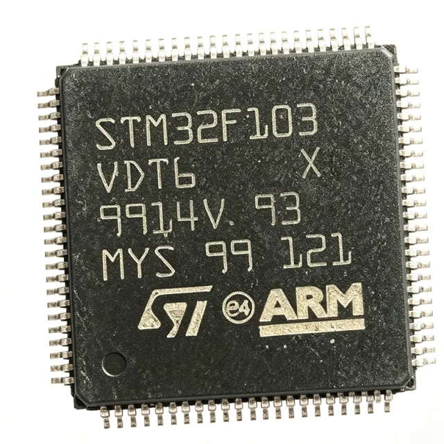
STM32F103VDT6 - 32-bit ARM Cortex-M3 MCU, 384KB Flash | STMicroelectronics
MPN: STM32F103VDT6 ✓ Active| Qty | Unit Price | Extended |
|---|---|---|
| 1 | $12.2727 | $12.27 |
| 10 | $8.8636 | $88.64 |
| 100 | $7.8409 | $784.09 |
| 500 | $7.5 | $3,750.00 |
| 1,000 | $7.1591 | $7,159.10 |
STM32F103VDT6 Overview
An ARM Cortex-M3 microcontroller is a 32-bit RISC processor designed for embedded systems, offering a balance of performance, power efficiency, and rich peripheral integration. It is part of the ARM Cortex-M family, which is widely used in industrial control, consumer electronics, and IoT devices. The Cortex-M3 core includes a hardware multiply and divide unit, Nested Vectored Interrupt Controller (NVIC), and optional Memory Protection Unit (MPU), enabling deterministic and efficient real-time processing.
Key features of the STM32F103VDT6 include a 72 MHz CPU with 1.25 DMIPS/MHz, 384 KB Flash, 64 KB SRAM, and a comprehensive set of peripherals: three 12-bit ADCs, four general-purpose 16-bit timers, two advanced-control timers, multiple communication interfaces (USART, SPI, I2C, CAN, USB), and a DMA controller. The device also includes a real-time clock (RTC), a CRC calculation unit, and a serial wire debug (SWD) interface.
The STM32F103VDT6 is built on a 0.13 µm embedded Flash process, providing a good balance of performance and power consumption. It supports a wide supply voltage range of 2.0V to 3.6V, with multiple low-power modes (Sleep, Stop, Standby) to optimize energy usage. The rich peripheral set and large memory make it a versatile choice for complex applications.
Typical applications include industrial control systems, motor drives, PLCs, medical devices, consumer electronics, and IoT gateways. The device's CAN interface and multiple timers make it particularly well-suited for automotive and industrial networking applications.
When designing with this MCU, ensure proper decoupling of the power supply pins and a stable clock source. The internal RC oscillator can be used for basic operation, but an external crystal is recommended for applications requiring precise timing. The SWD interface should be brought out for programming and debugging.
Drop-in alternatives for STM32F103VDT6 — same package, pin-to-pin compatible. Different-package parts requiring PCB rework are excluded.
Variants in this series
Same-series models that are drop-in compatible with STM32F103VDT6 (same form factor and footprint) — differing in Flash Memory, Package, Core, Operating Temperature, SRAM.
Quick Comparison Tool — Select alternative parts for side-by-side comparison:
STM32F103VET6
✓ In Stock
$3.85 / Unit
View Datasheet →STM32F103VCT6
✓ In Stock
$2.68 / Unit
View Datasheet →STM32F103VBT6
✓ In Stock
$3.33 / Unit
View Datasheet →STM32F103V8T6
✓ In Stock
$4.4 / Unit
View Datasheet →GD32F103VET6
📋 Reference alternative (not in catalog)
GD32F103VCT6
📋 Reference alternative (not in catalog)
APM32F103VET6
📋 Reference alternative (not in catalog)
APM32F103VCT6
📋 Reference alternative (not in catalog)
STM32F103VDT6 Maximum Ratings & Electrical Characteristics
| Core | ARM Cortex-M3 |
| Max Clock Speed | 72 MHz |
| Flash Memory | 384 KB |
| SRAM | 64 KB |
| Supply Voltage | 2.0 V to 3.6 V |
| Package | LQFP100 (14x14 mm) |
| Operating Temperature | -40°C to +85°C |
| GPIO Pins | 80 |
| ADC | 3x 12-bit, 16 channels |
| Timers | 4x 16-bit general purpose, 2x advanced control |
| Communication Interfaces | 5x USART, 3x SPI, 2x I2C, 1x CAN, 1x USB 2.0 FS |
| DMA | 12 channels |
| RTC | Yes |
| Debug Interface | SWD, JTAG |
| RoHS Status | Compliant |
STM32F103VDT6 Pin Configuration
| Pin 1 | VBAT — Backup battery supply for RTC and backup registers |
| Pin 2 | PC13 — GPIO or RTC tamper/calendar output |
| Pin 3 | PC14 — GPIO or OSC32_IN (32.768 kHz crystal input) |
| Pin 4 | PC15 — GPIO or OSC32_OUT (32.768 kHz crystal output) |
| Pin 5 | PD0 — GPIO or OSC_IN (main crystal input) |
| Pin 6 | PD1 — GPIO or OSC_OUT (main crystal output) |
| Pin 7 | NRST — Reset (active low) |
| Pin 8 | VSSA — Analog ground |
| Pin 9 | VDDA — Analog power supply (2.0V-3.6V) |
| Pin 10 | PA0 — GPIO/ADC12_IN0/TIM2_CH1 |
| Pin 11 | PA1 — GPIO/ADC12_IN1/TIM2_CH2 |
| Pin 12 | PA2 — GPIO/ADC12_IN2/TIM2_CH3/USART2_TX |
| Pin 13 | PA3 — GPIO/ADC12_IN3/TIM2_CH4/USART2_RX |
| Pin 14 | PA4 — GPIO/ADC12_IN4/SPI1_NSS |
| Pin 15 | PA5 — GPIO/ADC12_IN5/SPI1_SCK |
| Pin 16 | PA6 — GPIO/ADC12_IN6/SPI1_MISO |
| Pin 17 | PA7 — GPIO/ADC12_IN7/SPI1_MOSI |
| Pin 18 | PB0 — GPIO/ADC12_IN8/TIM3_CH3 |
| Pin 19 | PB1 — GPIO/ADC12_IN9/TIM3_CH4 |
| Pin 20 | PB2 — GPIO/BOOT1 |
Typical Applications
STM32F103VDT6 is suitable for 6 applications: Industrial Control Systems, Motor Drives, Medical Devices, Consumer Electronics, IoT Gateways, Automotive Electronics.
Industrial Control Systems
The STM32F103VDT6 is ideal for industrial control systems due to its rich peripheral set, including multiple timers, ADCs, and communication interfaces. Its 72 MHz Cortex-M3 core provides sufficient processing power for real-time control loops, while the CAN interface enables robust networking in factory automation. The device's wide operating temperature range (-40°C to +85°C) ensures reliability in harsh industrial environments. In a typical PLC application, the MCU reads sensor inputs via ADCs, executes control algorithms, and drives actuators through PWM outputs. The advanced-control timers (TIM1 and TIM8) generate precise PWM signals with dead-time insertion, essential for motor drives. The multiple USART and SPI interfaces allow connection to HMI panels, encoders, and other peripherals. The 384 KB Flash provides ample space for complex firmware, and the 64 KB SRAM supports real-time data buffering. The STM32F103VDT6's robust design and long-term availability make it a trusted choice for industrial applications.
Recommended
Motor Drives
The STM32F103VDT6 excels in motor drive applications, particularly for brushless DC (BLDC) and permanent magnet synchronous motors (PMSM). Its advanced-control timers (TIM1 and TIM8) provide six-channel PWM outputs with complementary signals and dead-time insertion, which are essential for driving three-phase inverters. The three 12-bit ADCs can sample motor currents and DC bus voltage simultaneously, enabling field-oriented control (FOC) algorithms. The 72 MHz CPU can execute FOC loops at high update rates, ensuring smooth and efficient motor operation. In a typical motor drive, the MCU reads Hall sensors or encoder feedback, computes the rotor position, and generates PWM signals to control the inverter switches. The CAN interface allows communication with a central controller for coordinated multi-axis motion. The device's robust timer and ADC features, combined with its industrial temperature range, make it a preferred choice for motor control in robotics, CNC machines, and electric vehicles.
Recommended
Medical Devices
The STM32F103VDT6 is suitable for medical devices such as patient monitors, infusion pumps, and diagnostic equipment. Its low power consumption and multiple low-power modes (Sleep, Stop, Standby) help extend battery life in portable devices. The device's rich analog peripherals, including three 12-bit ADCs, enable precise sensor measurements for vital sign monitoring. The 384 KB Flash allows storage of complex algorithms and patient data logs. In a patient monitor, the MCU acquires ECG, SpO2, and blood pressure signals through ADCs, processes them using digital signal processing techniques, and displays results on an LCD. The I2C and SPI interfaces connect to external sensors and display modules. The USB interface enables data transfer to a PC for further analysis. The STM32F103VDT6's reliability and long-term availability are critical for medical applications, where product lifecycle and regulatory compliance are paramount.
Recommended
Consumer Electronics
The STM32F103VDT6 is widely used in consumer electronics such as smart home devices, wearables, and audio equipment. Its rich peripheral set and low cost make it an attractive choice for mass-produced products. The device's USB 2.0 Full-Speed interface enables easy connectivity to PCs and smartphones for charging and data transfer. In a smart home hub, the MCU manages multiple communication protocols (Wi-Fi, Zigbee, Bluetooth) via external modules, processes sensor data, and controls actuators. The 384 KB Flash provides ample space for firmware updates over-the-air (OTA). The device's multiple timers and PWM outputs can drive LEDs, buzzers, and small motors. The STM32F103VDT6's balance of performance, memory, and cost makes it ideal for consumer products that require a feature-rich yet affordable microcontroller.
Recommended
IoT Gateways
The STM32F103VDT6 is well-suited for IoT gateways that aggregate data from multiple sensors and communicate with cloud services. Its multiple USART, SPI, and I2C interfaces allow connection to various sensors and communication modules (e.g., LoRa, NB-IoT, Wi-Fi). The CAN interface is useful for industrial IoT applications where legacy fieldbus integration is required. The device's 384 KB Flash and 64 KB SRAM can handle protocol stacks and data buffering. In a typical IoT gateway, the MCU collects data from sensors via UART or SPI, processes and filters it, and forwards it to a cloud server via an Ethernet or cellular module. The low-power modes help reduce energy consumption in battery-powered gateways. The STM32F103VDT6's robust communication capabilities and processing power make it a reliable choice for edge computing in IoT deployments.
Recommended
Automotive Electronics
The STM32F103VDT6 is used in automotive electronics such as body control modules, dashboard clusters, and infotainment systems. Its CAN interface is essential for communication with the vehicle's CAN bus network. The device's wide operating temperature range (-40°C to +85°C) and robust design meet automotive requirements. In a body control module, the MCU manages lighting, windows, and door locks, reading inputs from switches and sensors and driving outputs via relays or MOSFETs. The multiple timers and PWM outputs control LED lighting with dimming. The 384 KB Flash stores configuration data and diagnostic routines. The STM32F103VDT6's automotive-grade variants (e.g., STM32F103VDT6TR) are AEC-Q100 qualified, ensuring reliability in harsh automotive environments. Its long-term availability and comprehensive peripheral set make it a trusted choice for automotive electronics.
Recommended
Recommended Products Summary
Engineering reference data for STM32F103VDT6 — comparison, design guidance, and compliance information.
Selection Guide
Comparison with Alternatives
| Parameter | This Product | STM32F103VET6 | STM32F103VCT6 | GD32F103VET6 |
|---|---|---|---|---|
| Package | LQFP100 | LQFP100 | LQFP100 | LQFP100 |
| Brand | STMicroelectronics | STMicroelectronics | STMicroelectronics | GigaDevice |
| Core | ARM Cortex-M3 | ARM Cortex-M3 | ARM Cortex-M3 | ARM Cortex-M3 |
| Max Clock Speed | 72 MHz | 72 MHz | 72 MHz | 108 MHz |
| Flash Memory | 384 KB | 512 KB | 256 KB | 512 KB |
| SRAM | 64 KB | 64 KB | 48 KB | 64 KB |
| Supply Voltage | 2.0V to 3.6V | 2.0V to 3.6V | 2.0V to 3.6V | 2.6V to 3.6V |
| Operating Temperature | -40°C to +85°C | -40°C to +85°C | -40°C to +85°C | -40°C to +85°C |
Key Differentiators
- Higher Flash memory than STM32F103VCT6 (vs STM32F103VCT6)
- Pin-compatible with higher-memory VET6 (vs STM32F103VET6)
- Cross-brand compatibility with GigaDevice GD32F103 (vs GD32F103VET6)
Design Notes
Decouple each VDD pin with a 100nF ceramic capacitor placed as close to the pin as possible. Additionally, use a 4.7uF or larger bulk capacitor on the main power rail. The VDDA pin should be connected to VDD through a ferrite bead or low-pass filter to reduce noise on the analog supply. Ensure the VBAT pin is connected to a backup battery or tied to VDD if not used.
For the LQFP100 package, ensure proper solder pad design with a 0.5mm pitch. Use a 4-layer PCB with a solid ground plane for best EMC performance. Place the crystal oscillator (8 MHz) and its load capacitors close to the OSC_IN/OSC_OUT pins (PD0/PD1) to minimize parasitic capacitance and ensure stable oscillation. Keep high-speed traces away from the crystal and analog pins.
Do not leave the BOOT0 pin floating; tie it to ground through a 10k resistor for normal boot from Flash. Ensure the NRST pin has a 100nF capacitor to ground and a 10k pull-up resistor to VDD. When using the internal RC oscillator, note that its accuracy is ±1% over temperature, which may not be sufficient for CAN or USB communication; use an external crystal for these interfaces.
Compliance Information
RoHS compliant per STMicroelectronics product page. Not AEC-Q100 qualified for standard version; automotive-grade variants (e.g., STM32F103VDT6TR) are available.