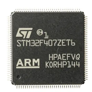
STM32F207ZGT6 - 32-bit ARM Cortex-M3 MCU, 1MB Flash | STMicroelectronics
MPN: STM32F207ZGT6 ✓ Active| Qty | Unit Price | Extended |
|---|---|---|
| 1 | $12.5 | $12.50 |
| 10 | $11.25 | $112.50 |
| 100 | $9.8 | $980.00 |
| 500 | $8.9 | $4,450.00 |
| 1,000 | $8.1 | $8,100.00 |
STM32F207ZGT6 Overview
A microcontroller (MCU) is a compact integrated circuit designed to govern a specific operation in an embedded system. It contains a processor core, memory (Flash and SRAM), and programmable input/output peripherals. The STM32F207ZGT6 belongs to the STM32F2 series, which is part of the broader STM32 family of 32-bit Flash microcontrollers. This family is widely used in industrial control, consumer electronics, and IoT devices due to its balance of performance, power efficiency, and peripheral integration.
Key features of the STM32F207ZGT6 include a 120 MHz ARM Cortex-M3 core with 1.25 DMIPS/MHz, 1 MB of Flash memory, 128 KB of SRAM, and a comprehensive set of peripherals: 3x 12-bit ADCs, 2x DACs, 4x USARTs, 2x UARTs, 3x SPI, 2x I2C, 2x CAN, 1x USB 2.0 OTG FS/HS, 1x Ethernet MAC, and a camera interface. It also features a flexible memory controller (FMC) for external memory expansion, a true random number generator (RNG), and a cryptographic acceleration cell for AES, DES, and 3DES.
The STM32F207ZGT6 is built on a 90nm process technology, offering a good balance between performance and power consumption. It operates from a 1.8V to 3.6V power supply and supports a wide temperature range of -40°C to +85°C. The device includes multiple low-power modes (Sleep, Stop, Standby) to optimize energy consumption in battery-powered applications.
Typical applications include industrial automation, motor control, medical devices, point-of-sale terminals, and IoT gateways. The Ethernet MAC and USB OTG support enable connectivity in networked systems, while the rich analog peripherals suit data acquisition and control loops.
When designing with this MCU, ensure proper decoupling of the power supply pins and a stable clock source. The device supports external crystal oscillators (4-26 MHz) and an internal 16 MHz RC oscillator. For high-speed USB and Ethernet, an external 25 MHz crystal is recommended. The boot pins must be configured correctly for programming via USART or USB.
Drop-in alternatives for STM32F207ZGT6 — same package, pin-to-pin compatible. Different-package parts requiring PCB rework are excluded.
Variants in this series
Same-series models that are drop-in compatible with STM32F207ZGT6 (same form factor and footprint) — differing in Ethernet, Flash Memory, Operating Temperature, Supply Voltage.
Quick Comparison Tool — Select alternative parts for side-by-side comparison:
STM32F207ZGT6
✅ Drop-In✓ In Stock
$8.1 / Unit
View Datasheet →STM32F207ZGT6TR
✅ Drop-In📋 Reference alternative (not in catalog)
STM32F207ZGT6
✅ Drop-In✓ In Stock
$8.1 / Unit
View Datasheet →STM32F207ZGT6
✅ Drop-In✓ In Stock
$8.1 / Unit
View Datasheet →STM32F207ZGT6
✅ Drop-In✓ In Stock
$8.1 / Unit
View Datasheet →STM32F207ZGT6
✅ Drop-In✓ In Stock
$8.1 / Unit
View Datasheet →STM32F207ZGT6
✅ Drop-In✓ In Stock
$8.1 / Unit
View Datasheet →STM32F207ZGT6
✅ Drop-In✓ In Stock
$8.1 / Unit
View Datasheet →STM32F207ZGT6
✅ Drop-In✓ In Stock
$8.1 / Unit
View Datasheet →STM32F207ZGT6
✅ Drop-In✓ In Stock
$8.1 / Unit
View Datasheet →STM32F207ZGT6
✅ Drop-In✓ In Stock
$8.1 / Unit
View Datasheet →STM32F207ZGT6
✅ Drop-In✓ In Stock
$8.1 / Unit
View Datasheet →STM32F207ZGT6
✅ Drop-In✓ In Stock
$8.1 / Unit
View Datasheet →STM32F207ZGT6
✅ Drop-In✓ In Stock
$8.1 / Unit
View Datasheet →STM32F207ZGT6
✅ Drop-In✓ In Stock
$8.1 / Unit
View Datasheet →STM32F207ZGT6
✅ Drop-In✓ In Stock
$8.1 / Unit
View Datasheet →STM32F207ZGT6
✅ Drop-In✓ In Stock
$8.1 / Unit
View Datasheet →STM32F207ZGT6
✅ Drop-In✓ In Stock
$8.1 / Unit
View Datasheet →STM32F207ZGT6
✅ Drop-In✓ In Stock
$8.1 / Unit
View Datasheet →STM32F207ZGT6
✅ Drop-In✓ In Stock
$8.1 / Unit
View Datasheet →STM32F207ZGT6 Maximum Ratings & Electrical Characteristics
| Core | ARM Cortex-M3 |
| Max Clock Frequency | 120 MHz |
| Flash Memory | 1 MB |
| SRAM | 128 KB |
| Supply Voltage | 1.8 V to 3.6 V |
| Operating Temperature | -40C to +85C |
| Package | LQFP144 (20x20 mm) |
| Number of I/O Pins | 114 |
| ADC | 3x 12-bit, up to 24 channels |
| DAC | 2x 12-bit |
| USART/UART | 4x USART, 2x UART |
| SPI | 3x SPI |
| I2C | 2x I2C |
| CAN | 2x CAN 2.0B |
| USB | USB 2.0 OTG FS/HS |
| Ethernet | 10/100 Ethernet MAC |
| Timers | 12x 16-bit, 2x 32-bit |
| DMA | 16-channel DMA |
| RTC | Yes |
| RoHS | Compliant |
STM32F207ZGT6 Pin Configuration
| Pin 1 | PE2 — GPIO or alternate function |
| Pin 2 | PE3 — GPIO or alternate function |
| Pin 3 | PE4 — GPIO or alternate function |
| Pin 4 | PE5 — GPIO or alternate function |
| Pin 5 | PE6 — GPIO or alternate function |
| Pin 6 | VBAT — Battery backup supply |
| Pin 7 | PC13 — GPIO or RTC output |
| Pin 8 | PC14 — GPIO or OSC32_IN |
| Pin 9 | PC15 — GPIO or OSC32_OUT |
| Pin 10 | PF0 — GPIO or OSC_IN |
| Pin 11 | PF1 — GPIO or OSC_OUT |
| Pin 12 | PF2 — GPIO |
| Pin 13 | PF3 — GPIO |
| Pin 14 | PF4 — GPIO |
| Pin 15 | PF5 — GPIO |
| Pin 16 | PF6 — GPIO |
| Pin 17 | PF7 — GPIO |
| Pin 18 | PF8 — GPIO |
| Pin 19 | PF9 — GPIO |
| Pin 20 | PF10 — GPIO |
| Pin 21 | VSS — Ground |
| Pin 22 | VDD — Power supply |
| Pin 23 | PF11 — GPIO |
| Pin 24 | PF12 — GPIO |
| Pin 25 | PF13 — GPIO |
| Pin 26 | PF14 — GPIO |
| Pin 27 | PF15 — GPIO |
| Pin 28 | PG0 — GPIO |
| Pin 29 | PG1 — GPIO |
| Pin 30 | PG2 — GPIO |
| Pin 31 | PG3 — GPIO |
| Pin 32 | PG4 — GPIO |
| Pin 33 | PG5 — GPIO |
| Pin 34 | PG6 — GPIO |
| Pin 35 | PG7 — GPIO |
| Pin 36 | PG8 — GPIO |
| Pin 37 | PG9 — GPIO |
| Pin 38 | PG10 — GPIO |
| Pin 39 | PG11 — GPIO |
| Pin 40 | PG12 — GPIO |
| Pin 41 | PG13 — GPIO |
| Pin 42 | PG14 — GPIO |
| Pin 43 | PG15 — GPIO |
| Pin 44 | VSS — Ground |
| Pin 45 | VDD — Power supply |
| Pin 46 | PD0 — GPIO or OSC_IN |
| Pin 47 | PD1 — GPIO or OSC_OUT |
| Pin 48 | PD2 — GPIO |
| Pin 49 | PD3 — GPIO |
| Pin 50 | PD4 — GPIO |
| Pin 51 | PD5 — GPIO |
| Pin 52 | PD6 — GPIO |
| Pin 53 | PD7 — GPIO |
| Pin 54 | PD8 — GPIO |
| Pin 55 | PD9 — GPIO |
| Pin 56 | PD10 — GPIO |
| Pin 57 | PD11 — GPIO |
| Pin 58 | PD12 — GPIO |
| Pin 59 | PD13 — GPIO |
| Pin 60 | PD14 — GPIO |
| Pin 61 | PD15 — GPIO |
| Pin 62 | PC0 — GPIO or ADC input |
| Pin 63 | PC1 — GPIO or ADC input |
| Pin 64 | PC2 — GPIO or ADC input |
| Pin 65 | PC3 — GPIO or ADC input |
| Pin 66 | VSSA — Analog ground |
| Pin 67 | VDDA — Analog power supply |
| Pin 68 | PC4 — GPIO or ADC input |
| Pin 69 | PC5 — GPIO or ADC input |
| Pin 70 | PB0 — GPIO or ADC input |
| Pin 71 | PB1 — GPIO or ADC input |
| Pin 72 | PB2 — GPIO |
| Pin 73 | PB3 — GPIO or JTDO |
| Pin 74 | PB4 — GPIO or NJTRST |
| Pin 75 | PB5 — GPIO |
| Pin 76 | PB6 — GPIO or I2C1_SCL |
| Pin 77 | PB7 — GPIO or I2C1_SDA |
| Pin 78 | BOOT0 — Boot mode selection |
| Pin 79 | PB8 — GPIO or I2C1_SCL |
| Pin 80 | PB9 — GPIO or I2C1_SDA |
| Pin 81 | PE0 — GPIO |
| Pin 82 | PE1 — GPIO |
| Pin 83 | VSS — Ground |
| Pin 84 | VDD — Power supply |
| Pin 85 | PE7 — GPIO |
| Pin 86 | PE8 — GPIO |
| Pin 87 | PE9 — GPIO |
| Pin 88 | PE10 — GPIO |
| Pin 89 | PE11 — GPIO |
| Pin 90 | PE12 — GPIO |
| Pin 91 | PE13 — GPIO |
| Pin 92 | PE14 — GPIO |
| Pin 93 | PE15 — GPIO |
| Pin 94 | PB10 — GPIO or I2C2_SCL |
| Pin 95 | PB11 — GPIO or I2C2_SDA |
| Pin 96 | PB12 — GPIO or SPI2_NSS |
| Pin 97 | PB13 — GPIO or SPI2_SCK |
| Pin 98 | PB14 — GPIO or SPI2_MISO |
| Pin 99 | PB15 — GPIO or SPI2_MOSI |
| Pin 100 | PD8 — GPIO or USART3_TX |
| Pin 101 | PD9 — GPIO or USART3_RX |
| Pin 102 | PD10 — GPIO or USART3_CK |
| Pin 103 | PD11 — GPIO or USART3_CTS |
| Pin 104 | PD12 — GPIO or USART3_RTS |
| Pin 105 | PD13 — GPIO |
| Pin 106 | PD14 — GPIO |
| Pin 107 | PD15 — GPIO |
| Pin 108 | PC6 — GPIO or I2S2_MCK |
| Pin 109 | PC7 — GPIO or I2S2_SCK |
| Pin 110 | PC8 — GPIO or I2S2_SD |
| Pin 111 | PC9 — GPIO or I2S2_WS |
| Pin 112 | PA0 — GPIO or ADC input |
| Pin 113 | PA1 — GPIO or ADC input |
| Pin 114 | PA2 — GPIO or ADC input |
| Pin 115 | PA3 — GPIO or ADC input |
| Pin 116 | VSS — Ground |
| Pin 117 | VDD — Power supply |
| Pin 118 | PA4 — GPIO or DAC_OUT1 |
| Pin 119 | PA5 — GPIO or DAC_OUT2 |
| Pin 120 | PA6 — GPIO |
| Pin 121 | PA7 — GPIO |
| Pin 122 | PA8 — GPIO |
| Pin 123 | PA9 — GPIO or USART1_TX |
| Pin 124 | PA10 — GPIO or USART1_RX |
| Pin 125 | PA11 — GPIO or USB_DM |
| Pin 126 | PA12 — GPIO or USB_DP |
| Pin 127 | PA13 — GPIO or JTMS/SWDIO |
| Pin 128 | PA14 — GPIO or JTCK/SWCLK |
| Pin 129 | PA15 — GPIO or JTDI |
| Pin 130 | PC10 — GPIO |
| Pin 131 | PC11 — GPIO |
| Pin 132 | PC12 — GPIO |
| Pin 133 | PD0 — GPIO or OSC_IN |
| Pin 134 | PD1 — GPIO or OSC_OUT |
| Pin 135 | PD2 — GPIO |
| Pin 136 | PD3 — GPIO |
| Pin 137 | PD4 — GPIO |
| Pin 138 | PD5 — GPIO |
| Pin 139 | PD6 — GPIO |
| Pin 140 | PD7 — GPIO |
| Pin 141 | VSS — Ground |
| Pin 142 | VDD — Power supply |
| Pin 143 | PB12 — GPIO or SPI2_NSS |
| Pin 144 | PB13 — GPIO or SPI2_SCK |
Typical Applications
STM32F207ZGT6 is suitable for 6 applications: Industrial Automation, IoT Gateway, Motor Control, Medical Devices, Point-of-Sale (POS) Terminals, Audio Processing.
Industrial Automation
The STM32F207ZGT6 is ideal for industrial automation due to its 120 MHz Cortex-M3 core, rich communication interfaces (CAN, UART, SPI, I2C), and advanced timers for PWM generation. It can handle real-time control loops, motor control, and PLC I/O modules. The device's 1 MB Flash allows storing complex control algorithms and communication stacks. Its wide operating temperature range (-40°C to +85°C) ensures reliability in harsh industrial environments. The Ethernet MAC enables connectivity to industrial networks like EtherCAT or PROFINET when paired with an external PHY. The multiple ADCs and DACs facilitate analog signal acquisition and generation for process control.
Recommended
IoT Gateway
The STM32F207ZGT6 serves as a powerful IoT gateway MCU, connecting sensors and devices to the cloud. Its Ethernet MAC and USB OTG support wired and wireless connectivity (via external modules). The 1 MB Flash and 128 KB SRAM can run TCP/IP stacks (lwIP), MQTT, and TLS. The device's low-power modes help reduce energy consumption in always-on gateways. The multiple UARTs and SPI interfaces allow connection to various sensors and radio modules (e.g., Wi-Fi, LoRa). The cryptographic acceleration cell (AES, DES, 3DES) enhances security for data transmission. The RTC enables time-stamping of sensor data.
Recommended
Motor Control
The STM32F207ZGT6 is well-suited for motor control applications, including BLDC, PMSM, and stepper motors. Its advanced timers (TIM1, TIM8) generate high-resolution PWM signals with dead-time insertion, essential for driving power stages. The 12-bit ADCs sample motor currents and voltages for FOC (Field-Oriented Control) algorithms. The 120 MHz core provides sufficient computational power for real-time control loops. The device's multiple communication interfaces (CAN, UART) enable integration with motor drives and industrial networks. The DMA controller offloads data transfer, reducing CPU load. The device's robust design and wide temperature range make it suitable for industrial motor drives.
Recommended
Medical Devices
The STM32F207ZGT6 is used in medical devices such as patient monitors, infusion pumps, and diagnostic equipment. Its high processing power and rich analog peripherals (ADCs, DACs) enable precise signal acquisition and control. The device's 1 MB Flash allows storing complex algorithms for signal processing and user interfaces. The multiple communication interfaces (USB, UART, SPI) facilitate data transfer to host systems. The device's low-power modes are beneficial for battery-powered portable medical devices. The cryptographic acceleration cell can secure patient data. The device's reliability and long-term availability make it suitable for medical applications.
Recommended
Point-of-Sale (POS) Terminals
The STM32F207ZGT6 is ideal for POS terminals, providing the processing power and connectivity needed for payment transactions. Its Ethernet MAC and USB OTG support wired and wireless connectivity to payment networks. The device's 1 MB Flash can store payment application code and encryption keys. The cryptographic acceleration cell (AES, DES, 3DES) ensures secure transactions. The multiple UARTs and SPI interfaces connect to card readers, PIN pads, and displays. The device's rich peripheral set and 114 I/O pins allow flexible system design. The wide operating temperature range ensures reliable operation in retail environments.
Recommended
Audio Processing
The STM32F207ZGT6 can be used in audio processing applications such as audio interfaces, effects processors, and voice-controlled devices. Its 120 MHz Cortex-M3 core can handle audio DSP algorithms like filtering and equalization. The device's 2x 12-bit DACs can output analog audio signals, while the I2S interface (via SPI) connects to external audio codecs. The 1 MB Flash allows storing audio samples and processing code. The USB OTG supports audio streaming to/from a host. The device's low-latency interrupt handling ensures real-time audio processing. The cryptographic acceleration cell can be used for DRM protection.
Recommended
Recommended Products Summary
Engineering reference data for STM32F207ZGT6 — comparison, design guidance, and compliance information.
Selection Guide
Comparison with Alternatives
| Parameter | This Product | STM32F207ZGT6 | STM32F407ZGT6 | STM32F205ZGT6 |
|---|---|---|---|---|
| Package | LQFP144 | LQFP144 | LQFP144 | LQFP144 |
| Brand | STMicroelectronics | STMicroelectronics | STMicroelectronics | STMicroelectronics |
| Core | ARM Cortex-M3 | ARM Cortex-M3 | ARM Cortex-M4 with FPU | ARM Cortex-M3 |
| Max Clock Frequency | 120 MHz | 120 MHz | 168 MHz | 120 MHz |
| Flash Memory | 1 MB | 1 MB | 1 MB | 1 MB |
| SRAM | 128 KB | 128 KB | 128 KB | 128 KB |
| Ethernet MAC | Yes | Yes | Yes | No |
| USB OTG | FS/HS | FS/HS | FS/HS | FS/HS |
| Price (1pc) | $12.50 | $12.50 | $14.20 | $11.80 |
Key Differentiators
- Higher clock frequency than STM32F205ZGT6 (vs STM32F205ZGT6)
- Ethernet MAC included (vs STM32F205ZGT6)
- Lower power consumption than STM32F407ZGT6 (vs STM32F407ZGT6)
Design Notes
The STM32F207ZGT6 requires a stable 3.3V supply. Decouple each VDD pin with a 100nF ceramic capacitor placed as close as possible to the pin, and add a 4.7uF bulk capacitor at the power entry. The VDDA pin should be filtered with a ferrite bead and a 1uF capacitor to reduce analog noise. Ensure the VDD and VDDA voltages are within 1.8V to 3.6V range.
For high-speed USB and Ethernet, use a 25 MHz crystal with load capacitors as specified in the datasheet. Keep the crystal traces short and away from high-speed digital signals. For the LQFP144 package, ensure proper solder paste stencil design for the 0.5mm pitch pins. Use a 4-layer PCB with a solid ground plane for best EMC performance.
Do not forget to configure the boot pins (BOOT0 and BOOT1) correctly. For normal operation, BOOT0 should be tied low. When programming via USART, BOOT0 must be high. Also, ensure the NRST pin has a 100nF capacitor to ground for reliable reset. The VCAP pins (if present) require a 2.2uF capacitor to ground for internal regulator stability.
Compliance Information
RoHS and REACH compliant per STMicroelectronics. Not AEC-Q100 qualified; for automotive use, consider STM32F207ZGT6Q or similar.