STP8N60M2 - 600V 8A N-Channel Power MOSFET | STMicroelectronics
MPN: STP8N60M2 ✓ Active| Qty | Unit Price | Extended |
|---|---|---|
| 1 | $1.25 | $1.25 |
| 10 | $1.12 | $11.20 |
| 100 | $0.98 | $98.00 |
| 500 | $0.85 | $425.00 |
| 1,000 | $0.75 | $750.00 |
STP8N60M2 Overview
A power MOSFET is a type of field-effect transistor designed to handle significant power levels, typically used as a switch in power electronics. It operates by controlling the voltage on the gate terminal to modulate the conductivity between the drain and source. Power MOSFETs are fundamental building blocks in switch-mode power supplies, motor drives, and lighting systems, where they enable efficient switching at high frequencies. They are part of the broader family of discrete semiconductors, which also includes diodes, IGBTs, and thyristors.
Key features of the STP8N60M2 include a very low gate charge (16nC) for reduced switching losses, a high dv/dt capability for ruggedness, and 100% avalanche tested for reliability. The device also offers a wide operating temperature range from -55°C to +150°C, making it suitable for demanding industrial environments. The TO-220 package provides a low thermal resistance of 62.5°C/W (junction-to-ambient), allowing efficient heat dissipation with proper heatsinking.
The MDmesh M2 technology combines a vertical structure with a deep trench gate, resulting in a significant reduction in on-resistance and gate charge compared to conventional planar MOSFETs. This technology enables higher efficiency and lower switching losses, particularly in high-frequency applications. The device's fast body diode and low reverse recovery charge (Qrr) further enhance performance in bridge topologies.
Typical applications include switch-mode power supplies (SMPS), power factor correction (PFC) circuits, LED lighting drivers, and motor control. In an SMPS, the STP8N60M2 can be used as the main switching element in a flyback or forward converter, where its low RDS(on) minimizes conduction losses and its fast switching reduces transition losses. For PFC, the device's high voltage rating and low gate charge enable efficient boost converters operating at high frequencies.
When designing with this device, ensure adequate gate drive voltage (typically 10V) to fully enhance the channel and minimize on-resistance. A gate resistor in the range of 10-100Ω is recommended to control switching speed and reduce EMI. Proper PCB layout with short, wide traces for high-current paths and a low-inductance gate loop is essential for reliable operation.
Drop-in alternatives for STP8N60M2 — same package, pin-to-pin compatible. Different-package parts requiring PCB rework are excluded.
Quick Comparison Tool — Select alternative parts for side-by-side comparison:
STP8N60M2-1
✅ Drop-In📋 Reference alternative (not in catalog)
STP8N60M2FP
✅ Drop-In📋 Reference alternative (not in catalog)
STP8N60M2-1FP
✅ Drop-In📋 Reference alternative (not in catalog)
IPP60R099P7
✅ Drop-In ⚠️ Specs Unverified📋 Reference alternative (not in catalog)
FCP8N60N
✅ Drop-In ⚠️ Specs Unverified📋 Reference alternative (not in catalog)
STP8N60M2 Maximum Ratings & Electrical Characteristics
| Technology | MDmesh M2 |
| Drain-Source Voltage (VDS) | 600 V |
| Continuous Drain Current (ID) | 8 A at 25°C |
| Pulsed Drain Current (IDM) | 32 A |
| On-Resistance (RDS(on)) | 0.55 Ω typical, 0.65 Ω max |
| Gate-Source Voltage (VGS) | ±25 V |
| Gate Charge (Qg) | 16 nC |
| Input Capacitance (Ciss) | 560 pF |
| Output Capacitance (Coss) | 45 pF |
| Reverse Transfer Capacitance (Crss) | 3.5 pF |
| Power Dissipation (PD) | 110 W at 25°C |
| Operating Temperature Range | -55°C to +150°C |
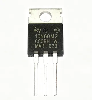
| Package | TO-220 |
| Mounting Type | Through Hole |
| Avalanche Energy (EAS) | 200 mJ |
| RoHS Status | Compliant |
STP8N60M2 Pin Configuration
| Pin 1 | Gate — Gate terminal for controlling the MOSFET |
| Pin 2 | Drain — Drain terminal, connected to the heat tab |
| Pin 3 | Source — Source terminal |
Safe Operating Area (DC)
Typical Applications
STP8N60M2 is suitable for 6 applications: Switch-Mode Power Supplies (SMPS), Power Factor Correction (PFC), LED Lighting Drivers, Motor Control, Solar Inverters, Welding Equipment.
Switch-Mode Power Supplies (SMPS)
The STP8N60M2 is ideal for SMPS topologies such as flyback and forward converters. Its 600V breakdown voltage and low on-resistance (0.55Ω) minimize conduction losses, while the low gate charge (16nC) enables high-frequency switching, reducing transformer size and improving power density. In a typical flyback converter, the MOSFET switches at frequencies up to 100kHz, and the device's fast switching characteristics ensure low switching losses. The TO-220 package allows efficient heat dissipation when mounted on a heatsink, ensuring reliable operation at power levels up to 110W. Compared to older planar MOSFETs, the MDmesh M2 technology reduces switching losses by up to 30%, making it a preferred choice for energy-efficient power supplies.
Recommended
Power Factor Correction (PFC)
In boost PFC circuits, the STP8N60M2 operates as the main switching element, shaping the input current to be sinusoidal and in phase with the voltage. The device's high voltage rating (600V) handles the boosted output voltage (typically 400V), while its low gate charge reduces drive losses at high switching frequencies (50-100kHz). The low reverse recovery charge (Qrr) of the body diode minimizes losses during the dead-time in continuous conduction mode. The MDmesh M2 technology provides a good trade-off between on-resistance and capacitance, resulting in high efficiency (typically >95%) in PFC stages. The TO-220 package is suitable for through-hole assembly, and the device's avalanche ruggedness ensures reliability during transient overvoltage conditions.
Recommended
LED Lighting Drivers
The STP8N60M2 is used in LED drivers for high-power lighting applications, such as street lights and industrial lighting. Its 600V rating allows direct connection to rectified AC mains (up to 265VAC), and the low on-resistance ensures high efficiency in constant-current topologies. The device's fast switching enables compact magnetic components, reducing the overall size of the driver. In a typical single-stage flyback LED driver, the MOSFET switches at 65kHz, and the low gate charge simplifies the gate drive circuit. The wide operating temperature range (-55°C to +150°C) ensures reliable operation in outdoor environments. The TO-220 package can be mounted on a heatsink to dissipate heat from the driver's power stage, ensuring long LED lifetime.
Recommended
Motor Control
In motor control applications, the STP8N60M2 is used in the inverter stage of variable frequency drives (VFDs) for induction motors and brushless DC motors. The device's 600V rating is suitable for 230VAC or 400VAC motor drives, and its low on-resistance reduces conduction losses in the high-current paths. The fast body diode and low Qrr enable efficient operation in bridge topologies, reducing dead-time losses. The device's avalanche ruggedness ensures reliability during motor start-up and stall conditions, where inductive spikes can occur. The TO-220 package is commonly used in motor drives, and the device can be paralleled to increase current capability. The MDmesh M2 technology provides a good balance between switching speed and EMI performance, making it suitable for PWM-controlled motor drives.
Recommended
Solar Inverters
The STP8N60M2 is used in solar micro-inverters and string inverters for DC-AC conversion. Its 600V rating handles the high DC bus voltage from solar panels (up to 450V), and the low on-resistance minimizes losses in the boost and inverter stages. The device's fast switching enables high-frequency operation, reducing the size of magnetics and improving power density. In a typical micro-inverter, the MOSFET operates in a full-bridge topology at 50kHz, and the low gate charge simplifies the gate drive design. The device's wide operating temperature range is suitable for outdoor installations, and the TO-220 package allows efficient heat dissipation. The MDmesh M2 technology ensures high efficiency (up to 98%) in solar applications, maximizing energy harvest.
Recommended
Welding Equipment
In inverter-based welding machines, the STP8N60M2 is used in the high-frequency switching stage to convert AC mains to a controlled DC output. The device's 600V rating and 8A current capability are suitable for medium-power welders (up to 200A output). The low on-resistance reduces conduction losses, and the fast switching enables high-frequency operation (up to 100kHz), reducing transformer size and weight. The device's ruggedness, including avalanche energy rating of 200mJ, ensures reliability under harsh load conditions. The TO-220 package is commonly used in welding equipment, and the device can be paralleled for higher current. The MDmesh M2 technology provides a good balance between efficiency and cost, making it a popular choice for welding inverter designs.
Recommended
Recommended Products Summary
Engineering reference data for STP8N60M2 — comparison, design guidance, and compliance information.
Selection Guide
Comparison with Alternatives
| Parameter | This Product | STP8N60M2-1 | STP8N60M2FP | IPP60R099P7 | FCP8N60N |
|---|---|---|---|---|---|
| Package | TO-220 | TO-220 | TO-220FP | TO-220 | TO-220 |
| Brand | STMicroelectronics | STMicroelectronics | STMicroelectronics | Infineon | onsemi |
| Drain-Source Voltage (VDS) | 600 V | 600 V | 600 V | 600 V | 600 V |
| Continuous Drain Current (ID) | 8 A | 8 A | 8 A | 8 A | 8 A |
| On-Resistance (RDS(on)) | 0.55 Ω | 0.55 Ω | 0.55 Ω | 0.099 Ω | 0.55 Ω |
| Gate Charge (Qg) | 16 nC | 16 nC | 16 nC | 30 nC | 20 nC |
| Power Dissipation (PD) | 110 W | 110 W | 35 W | 125 W | 110 W |
| Avalanche Energy (EAS) | 200 mJ | 200 mJ | 200 mJ | 150 mJ | 200 mJ |
Key Differentiators
- Low on-resistance of 0.55Ω typical (vs IPP60R099P7)
- Low gate charge of 16nC (vs FCP8N60N)
- Avalanche energy rating of 200mJ (vs IPP60R099P7)
Design Notes
The STP8N60M2 has a junction-to-case thermal resistance of 1.14°C/W and a maximum power dissipation of 110W at 25°C case temperature. For reliable operation, use a heatsink with a thermal resistance of less than 1°C/W for high-power applications. Ensure the case temperature does not exceed 100°C to maintain the device within its safe operating area.
For the TO-220 package, the drain tab is electrically connected to the drain terminal. When mounting on a heatsink, use an insulating pad and thermal compound to avoid short circuits. Keep the gate drive traces short and direct to minimize parasitic inductance, and place a gate resistor (10-100Ω) close to the gate pin to control switching speed and reduce EMI.
Do not exceed the maximum gate-source voltage of ±25V. Use a gate clamp or zener diode to protect against overvoltage spikes. Ensure the gate drive voltage is at least 10V to fully enhance the channel and achieve the specified on-resistance. Also, consider the body diode's reverse recovery characteristics in bridge topologies; the STP8N60M2 has a fast body diode, but additional snubber circuits may be needed for high dv/dt conditions.
Compliance Information
RoHS compliant per STMicroelectronics. Not AEC-Q100 qualified; for automotive, consider AEC-Q101 qualified devices.