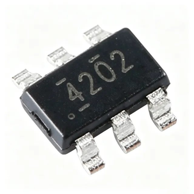
TPS54202DDCR - 4.5V-28V 2A Sync Buck Converter | TI
MPN: TPS54202DDCR ✓ Active| Qty | Unit Price | Extended |
|---|---|---|
| 1 | $0.62 | $0.62 |
| 10 | $0.51 | $5.10 |
| 100 | $0.38 | $38.00 |
| 500 | $0.25 | $125.00 |
| 1,000 | $0.17 | $170.00 |
| 3,000 | $0.12 | $360.00 |
TPS54202DDCR Overview
A buck (step-down) converter is a DC-DC switching regulator that efficiently converts a higher input voltage to a lower output voltage using inductive energy storage and high-frequency switching. Unlike linear regulators, buck converters achieve high efficiency even with large input-to-output voltage differentials. As a synchronous buck, the TPS54202 replaces the freewheeling Schottky diode with an integrated low-side MOSFET, improving light-load and full-load efficiency within the power management IC family.
Key features include the adjustable output range of 0.596V to 26V, a fixed 500kHz switching frequency, and Advanced Eco-mode operation that folds back switching frequency at light loads to extend standby efficiency. The 45uA quiescent current suits always-on and battery-backed systems. EMI-friendly design techniques ease EMC compliance, and integrated overcurrent and thermal shutdown protection ensure robustness. The -40C to +125C junction temperature range supports industrial environments.
Architecturally, the device uses current-mode control with internal compensation, so no external compensation network is needed. Integrated low-RDS(on) MOSFETs deliver high efficiency in the small SOT-23-6 thin package, achieving high power density without a heatsink at moderate loads.
Typical applications include 12V and 24V rail point-of-load conversion in set-top boxes, broadband and networking equipment, industrial supplies, and portable instruments. For example, it efficiently steps 12V down to 3.3V for digital logic with minimal ripple.
Design tip: follow the datasheet recommendation of a 10uF input and 22uF output ceramic capacitor, and keep the SW/BOOT loops tight on the PCB; verify thermal relief on the exposed area for loads above 1.5A.
Drop-in alternatives for TPS54202DDCR — same package, pin-to-pin compatible. Different-package parts requiring PCB rework are excluded.
Variants in this series
Same-series models that are drop-in compatible with TPS54202DDCR (same form factor and footprint) — differing in Maximum Output Current, Package, Switching Frequency, Input Voltage Range, Operating Temperature.
Quick Comparison Tool — Select alternative parts for side-by-side comparison:
TPS542021DDCR
✅ Drop-In📋 Reference alternative (not in catalog)
TPS54202HDDCR
✅ Drop-In📋 Reference alternative (not in catalog)
TPS54302DDCRQ1
✅ Drop-In📋 Reference alternative (not in catalog)
TPS561201DDCR
✅ Drop-In✓ In Stock
$0.29 / Unit
View Datasheet →RT8299A
⚡ Same Package ⚠️ Specs Unverified📋 Reference alternative (not in catalog)
TPS54202DDCR Maximum Ratings & Electrical Characteristics
| Topology | Synchronous Buck (Step-Down) |
| Input Voltage Range | 4.5 V to 28 V |
| Maximum Output Current | 2 A |
| Output Voltage Range | 0.596 V adjustable |
| Number of Outputs | 1 |
| Switching Frequency | 500 kHz |
| Quiescent Current | 45 uA |
| Control Topology | Current-mode with internal compensation |
| Internal Soft Start | 5 ms |
| Light Load Mode | Advanced Eco-mode |
| Integrated MOSFETs | Yes (high-side and low-side) |
| Operating Temperature | -40C to +125C (TJ) |
| Package | SOT-23-6 Thin (DDC / TSOT-23-6) |
| Mounting Style | SMD/SMT |
| Protection Features | Overcurrent, thermal shutdown |
| RoHS Status | Compliant |
TPS54202DDCR Pin Configuration
| Pin 1 | BOOT — Bootstrap capacitor connection for high-side gate drive |
| Pin 2 | VIN — Input supply, 4.5V to 28V |
| Pin 3 | EN — Enable pin with internal pullup (adjustable UVLO via divider) |
| Pin 4 | FB — Feedback input for output voltage adjustment |
| Pin 5 | GND — Ground |
| Pin 6 | SW — Switch node to power inductor |
Typical Applications
TPS54202DDCR is suitable for 6 applications: Industrial 24V Point-of-Load Power, Networking and Broadband Equipment, Battery-Backed and Always-On Systems, Automotive Auxiliary Power, Portable and Test Instruments, Set-Top Box and Consumer Media Power.
Industrial 24V Point-of-Load Power
The TPS54202DDCR's 28V maximum input accommodates 24V industrial buses with headroom, converting down to 3.3V or 5V at up to 2A for PLC I/O modules, sensors, and control logic. Its 500kHz fixed frequency allows a small inductor, while integrated compensation removes external RC networks. Overcurrent and thermal shutdown protect against field faults, and the -40C to +125C junction range covers unconditioned cabinet environments.
Recommended
Networking and Broadband Equipment
Set-top boxes, routers, and broadband CPE step 12V wall-adapter inputs to 3.3V/1.8V logic rails. The TPS54202DDCR's Advanced Eco-mode folds switching frequency at standby, cutting no-load input power to meet energy-efficiency requirements, while 45uA quiescent current minimizes always-on drain. EMI-friendly switching-edge control eases FCC/CISPR conducted-emissions compliance without heavy shielding in plastic enclosures.
Recommended
Battery-Backed and Always-On Systems
With only 45uA quiescent current and Eco-mode pulse-skipping, the TPS54202DDCR sustains high efficiency down to milliamp loads in metering, alarm panels, and backup-power modules. The 5ms internal soft start limits inrush when switching to battery, and the adjustable 0.596V reference supports lithium-cell and lead-acid derived rails. Designers should size the output capacitor for stable Eco-mode operation at light load.
Recommended
Automotive Auxiliary Power
For automotive modules needing a qualified 2A buck, the pin-compatible AEC-Q100 TPS54202HDDCR variant drops onto the same SOT-23-6 footprint, enabling one PCB design across industrial and automotive builds. The 28V input covers 12V battery rails including load-dump clamped conditions with a TVS; 500kHz operation keeps filter components compact for infotainment, telematics, and body-control auxiliary supplies.
Recommended
Portable and Test Instruments
Handheld meters and portable instruments benefit from the TPS54202DDCR's tiny 2.9mm x 2.9mm-class SOT-23-6 footprint and minimal external count - typically one inductor plus 10uF input and 22uF output ceramic capacitors. Internal compensation and soft start shorten design time, and the 0.596V feedback reference enables low-voltage processor rails. Thermal performance supports 2A bursts without heatsinking in enclosed handheld form factors.
Recommended
Set-Top Box and Consumer Media Power
Consumer media devices convert external 12V adapters to multiple low-voltage rails. The TPS54202DDCR provides the main 3.3V/5V rail at 2A with high full-load efficiency from integrated synchronous MOSFETs, while Eco-mode meets standby power codes. Fixed 500kHz switching keeps ripple above the AM band edge and simplifies EMI filtering on cost-sensitive two-layer consumer PCBs.
Recommended
Recommended Products Summary
Engineering reference data for TPS54202DDCR — comparison, design guidance, and compliance information.
Selection Guide
Comparison with Alternatives
| Parameter | This Product | TPS542021DDCR | TPS54202HDDCR | TPS54302DDCRQ1 | TPS561201DDCR | RT8299A |
|---|---|---|---|---|---|---|
| Package | SOT-23-6 Thin (DDC) | SOT-23-6 Thin (DDC) - same | SOT-23-6 Thin (DDC) - same | SOT-23-6 Thin (DDC) - same | SOT-23-6 Thin (DDC) - same | SOT-23-6 - same outline, different pinout |
| Brand | Texas Instruments | Texas Instruments | Texas Instruments | Texas Instruments | Texas Instruments | Richtek |
| Input Voltage Range | 4.5 V to 28 V | 4.5 V to 30 V | 4.5 V to 28 V | 4.5 V to 28 V | 4.5 V to 17 V | 4.5 V to 32 V |
| Output Current | 2 A | 2 A | 2 A | 3 A | 1 A | 2 A |
| Switching Frequency | 500 kHz | 500 kHz | 500 kHz | 500 kHz | 1.5 MHz | 380 kHz / 800 kHz selectable |
| Automotive Grade (AEC-Q100) | No | No | Yes | Yes | No | No |
| Lifecycle Status | Active | Active (new device) | Active | Active | Active | Active |
Key Differentiators
- Widest input range in same-package 2A family (vs TPS561201DDCR)
- Ultra-low standby consumption (vs RT8299A)
- Higher current drop-in path (vs TPS54302DDCRQ1)
Design Notes
Place the 10uF input ceramic capacitor as close as possible to the VIN and GND pins, and the 22uF output capacitor directly across the inductor output to GND. Keep the SW node, BOOT capacitor, and inductor loop area minimal - these carry 500kHz square-wave current and dominate radiated EMI. Use a solid ground plane and multiple vias under the IC ground connection per TI datasheet layout guidelines.
At 24V input stepping to 3.3V at 2A, conduction and switching losses can push junction temperature significantly in the small SOT-23-6 thin package. Calculate losses from the datasheet efficiency curves for your exact operating point and verify TJ stays below 125C at maximum ambient. Increase copper area tied to GND/SW and avoid placing the part near heat sources for designs operating above roughly 1.5A continuous output.
Do not exceed the 28V absolute maximum input - add a TVS clamp on 24V industrial buses exposed to transients. When substituting pin-compatible parts such as TPS54302 (3A) or TPS561201 (1A), re-verify output capacitor stability and EN threshold because internal parameters differ despite the shared SOT-23-6 footprint. Set the feedback divider with 1% resistors; the 0.596V reference means low-value top resistors minimize FB-node noise sensitivity.
Compliance Information
RoHS compliant per LCSC and JLCPCB listings (part C191884). AEC-Q100 not applicable to standard grade; use TPS54202HDDCR for automotive qualification.







