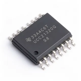
UCC21550AQDWKRQ1 - 4A/6A 5kVRMS Isolated Gate Driver | TI
MPN: UCC21550AQDWKRQ1 ✓ Active| Qty | Unit Price | Extended |
|---|---|---|
| 1 | $3.6 | $3.60 |
| 10 | $3.25 | $32.50 |
| 100 | $2.85 | $285.00 |
| 500 | $2.5 | $1,250.00 |
| 1,000 | $2.2 | $2,200.00 |
UCC21550AQDWKRQ1 Overview
An isolated gate driver is a power management IC that transfers logic-level PWM control signals across a galvanic isolation barrier to drive the gate of a power semiconductor operating at high voltage. In the power-electronics hierarchy, it sits between the PWM controller or MCU and the power stage (MOSFET, SiC MOSFET, GaN FET, or IGBT), providing both safety isolation and the high peak current needed to switch power devices quickly and efficiently.
Key features include the 4 A/6 A asymmetric drive strength that accelerates turn-off to reduce switching losses, 5 kVRMS reinforced isolation suitable for high-voltage industrial and automotive buses, and programmable dead time via a single resistor on the DT pin, which simplifies half-bridge design and protects against shoot-through. The DIS pin allows immediate output disable for fault handling.
Architecturally, the input side (INA, INB, DIS) uses TTL- and CMOS-compatible input thresholds isolated from the VDD supply. The UCC21550-Q1 can be configured as two low-side drivers, two high-side drivers, or a half-bridge driver, giving designers one part number for multiple topologies. Capacitive isolation technology provides high CMTI and long-term barrier reliability for automotive environments.
Typical applications include onboard chargers (OBC), traction inverters, and DC-DC converters in electric vehicles, as well as solar inverters, motor drives, and server/telecom power supplies where SiC or IGBT switches demand robust, isolated gate drive.
Design-wise, use the DT pin resistor to set dead time per your switch technology; SiC and GaN typically need shorter dead time than IGBTs. Ensure VDD decoupling with low-ESR ceramics close to the driver.
This page synthesizes distributor pricing, drop-in family alternatives, and practical design notes not found in the manufacturer datasheet.
Drop-in alternatives for UCC21550AQDWKRQ1 — same package, pin-to-pin compatible. Different-package parts requiring PCB rework are excluded.
Variants in this series
Same-series models that are drop-in compatible with UCC21550AQDWKRQ1 (same form factor and footprint) — differing in Disable Function, Configuration, Dead Time, Isolation Type, Package.
Quick Comparison Tool — Select alternative parts for side-by-side comparison:
UCC21550BQDWRQ1
✅ Drop-In✓ In Stock
$2.45 / Unit
View Datasheet →UCC21550AQDWQ1
✅ Drop-In ⚠️ Specs Unverified📋 Reference alternative (not in catalog)
UCC21550AQDWRQ1
✅ Drop-In ⚠️ Specs Unverified📋 Reference alternative (not in catalog)
UCC21550AQDWKRQ1 Maximum Ratings & Electrical Characteristics
| Product Type | Reinforced isolated dual-channel gate driver |
| Peak Source Current | 4 A |
| Peak Sink Current | 6 A |
| Number of Channels | 2 |
| Isolation Voltage | 5000 Vrms |
| Isolation Technology | Capacitive coupling |
| Configuration | Two low-side, two high-side, or half-bridge |
| Dead Time | Programmable via DT pin |
| Disable Function | Yes (DIS pin) |
| Input Threshold Logic | TTL and CMOS compatible |
| Target Switch Types | Power MOSFET, SiC, GaN, IGBT |
| Qualification | Automotive (Q1) |
| Package | 14-SOIC (DWK) |
| Part Marking | 21550AQ |
| Mounting Type | Surface Mount |
UCC21550AQDWKRQ1 14-soic (dwk) Pin Configuration Guide
Pin configuration for UCC21550AQDWKRQ1 (14-soic (dwk) package). This power device features gate, drain, and source terminals. For non-polarized packages, refer to the manufacturer datasheet for exact pin 1 orientation and footprint details. Common applications include power supply design, motor driving, and load switching.

No detailed pinout data available for UCC21550AQDWKRQ1.
Refer to the datasheet for full pin configuration.
Typical Applications
UCC21550AQDWKRQ1 is suitable for 6 applications: Automotive Onboard Charger (OBC), Traction Inverter / Motor Drive, Solar / String Inverter DC-DC Stage, Server and Telecom Power Supplies, GaN Fast Chargers and Adapters, Industrial Motor Drives and Servo Amplifiers.
Automotive Onboard Charger (OBC)
In an EV onboard charger, the PFC and LLC stages switch 400 V to 800 V bus voltages, so the gate driver must isolate the low-voltage MCU from the power stage while delivering enough current for fast, efficient switching. The UCC21550AQDWKRQ1 fits this role with its 5000 Vrms reinforced capacitive isolation barrier and 4 A source / 6 A sink drive, which sharpens SiC MOSFET switching transitions and reduces switching losses at 100 kHz+ LLC frequencies. The DT pin lets the designer program dead time with a single resistor to prevent shoot-through in the half-bridge LLC leg, while the DIS pin provides a fast hardware path to disable gates during fault events flagged by the controller. Configured as a half-bridge driver, one UCC21550-Q1 replaces two separate isolated drivers, saving board area in the compact OBC enclosure. Automotive Q1 qualification supports OBC production programs.
Recommended
Traction Inverter / Motor Drive
Traction inverters and industrial motor drives use three-phase half-bridge stages switching hundreds of amps at high bus voltage, where gate-drive robustness and barrier reliability are safety-critical. The UCC21550AQDWKRQ1 provides 5000 Vrms reinforced isolation between the controller domain and each gate, and its 6 A peak sink current pulls IGBT or SiC gates off quickly, minimizing tail-current and turn-off losses that dominate inverter efficiency. The programmable DT pin allows dead time to be tuned per switch technology - shorter for SiC to maximize modulation index, longer for IGBTs to absorb charge-storage delay. TTL/CMOS-compatible inputs connect directly to the C2000 MCU PWM outputs. Configurable as two high-side or half-bridge drivers, it supports flexible gate-drive partitioning across the three phases with a single, automotive-qualified part number.
Recommended
Solar / String Inverter DC-DC Stage
Grid-tied solar inverters boost the PV panel voltage and convert it through an isolated DC-DC stage, typically an LLC or phase-shifted full bridge using SiC MOSFETs or IGBTs at high switching frequency. The UCC21550AQDWKRQ1's 5000 Vrms reinforced isolation meets the galvanic separation required between the PV input and the grid-connected output, while capacitive isolation technology sustains the high dv/dt common-mode transients generated by fast switching bridges. The 4 A/6 A drive strength keeps SiC switching transitions sharp at 100 kHz and above, limiting magnetics and thermal stress. Programmable dead time via the DT pin protects against bridge shoot-through, and the DIS pin gives the system controller a deterministic gate-off path for MPPT fault handling or anti-islanding shutdown sequences.
Recommended
Server and Telecom Power Supplies
High-density server and telecom rectifiers use bridgeless PFC and LLC stages driven from digital power controllers, demanding compact, efficient isolated gate drive. The UCC21550AQDWKRQ1 integrates the isolation barrier and 4 A/6 A driver in one 14-pin SOIC, replacing discrete transformer-coupled drive circuits and shrinking solution size on the power board. Its programmable dead time allows the LLC burst-mode and phase-shift timing to be optimized in hardware with one resistor, while 5000 Vrms reinforced isolation satisfies safety separation for telecom -48 V and high-voltage DC bus architectures. The DIS pin supports fast output disable during hot-plug and protection events, and the wide-drive-current margin accommodates both SiC MOSFET and superjunction MOSFET gate charges found across 800 W to 3 kW power supply designs.
Recommended
GaN Fast Chargers and Adapters
High-frequency GaN-based charger and adapter designs switch at several hundred kilohertz to kilohertz ranges, where every nanosecond of gate-drive delay affects efficiency and thermal headroom. The UCC21550AQDWKRQ1's capacitive isolation adds minimal propagation delay while its 6 A peak sink current rapidly discharges the low gate charge of GaN FETs, preventing spurious turn-on from dv/dt-induced charge injection. The DT pin allows precise, short dead-time settings that GaN half-bridges require to exploit their zero-reverse-recovery behavior. Configured as a half-bridge driver, a single device manages both high-side and low-side gates across the 5000 Vrms barrier, keeping the control side safe. Although this orderable is automotive Q1 qualified, its performance envelope makes it equally suitable for premium consumer fast-charger power stages.
Recommended
Industrial Motor Drives and Servo Amplifiers
Industrial servo amplifiers and general-purpose motor drives switch IGBT or SiC power modules from a controller that must remain galvanically isolated from the high-voltage DC bus. The UCC21550AQDWKRQ1 provides that reinforced 5000 Vrms barrier plus 4 A/6 A gate drive, sufficient for the gate charges of 600 V to 1200 V switch ratings common in drives up to several kilowatts. The programmable dead time via the DT pin is essential here: IGBTs require deliberately longer interlock intervals to accommodate tail current, and the single-resistor setting simplifies design variants across drive power ratings. The DIS pin gives overcurrent protection logic a fast, deterministic shutdown path, and configuring the device as two low-side drivers suits common bus-capacitor and brake-chopper topologies alongside the main three-phase bridge.
Recommended
Recommended Products Summary
Engineering reference data for UCC21550AQDWKRQ1 — comparison, design guidance, and compliance information.
Selection Guide
Comparison with Alternatives
| Parameter | This Product | UCC21550BQDWRQ1 | UCC21550AQDWQ1 | UCC21550AQDWRQ1 |
|---|---|---|---|---|
| Package | 14-SOIC (DWK) | 14-SOIC (DW) | 14-SOIC (DW) | 14-SOIC (DW) |
| Brand | Texas Instruments | Texas Instruments | Texas Instruments | Texas Instruments |
| Peak Source / Sink Current | 4 A / 6 A | 4 A / 6 A | 4 A / 6 A | 4 A / 6 A |
| Isolation Voltage | 5000 Vrms | 5000 Vrms | 5000 Vrms | 5000 Vrms |
| Channels | 2 | 2 | 2 | 2 |
| Programmable Dead Time (DT pin) | Yes | Yes | Yes | Yes |
| Disable Pin (DIS) | Yes | Yes (variant-B behavior) | Yes | Yes |
| Automotive Qualification | Yes (Q1) | Yes (Q1) | Yes (Q1) | Yes (Q1) |
Key Differentiators
- Asymmetric 4 A source / 6 A sink drive strength (vs UCC21550BQDWRQ1)
- Programmable dead time with a single DT-pin resistor (vs Fixed-dead-time isolated drivers)
- One device covers low-side, high-side, and half-bridge topologies (vs Single-function dual drivers)
Design Notes
Verify the package suffix before layout release: this orderable uses the 14-pin SOIC DWK body, while sibling UCC21550-Q1 orderables (DW suffix) use the 14-SOIC DW body. Confirm the exact body dimensions and land pattern against the TI datasheet mechanical drawings - assuming the two footprints are identical risks rework on automotive builds. Also confirm the A-versus-B functional variant matches your DT and DIS pin expectations per the datasheet ordering table.
Place low-ESR ceramic decoupling capacitors (typical practice: 100 nF in parallel with a bulk value per the TI datasheet typical application) directly across VDDI and each output-side VDDA/VDDB pin to the driver ground, with the shortest possible loops. Route gate-drive traces as short, wide pairs with their return paths, and keep the DT pin resistor close to the device with a solid ground reference so the programmed dead time is not corrupted by gate-switching noise coupling.
Size the gate-drive energy budget per channel: estimated peak instantaneous gate power is Vgate_peak_drive times gate charge of your switch; the 4 A/6 A capability sets the minimum transition time as roughly Qg/Ipeak. For SiC MOSFETs in half-bridge use, program a short DT dead time; for IGBTs, allow a longer interval to cover tail-current delay and prevent shoot-through. Estimated guidance - confirm with the datasheet DT resistor equation for your exact timing target.
Compliance Information
Automotive Q1 qualification stated on TI product page. RoHS/REACH/lead-free/halogen-free status not explicitly stated in the captured web data - verify via TI product page environmental data.