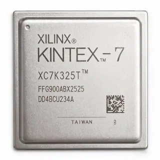
XC7K325T-3FFG900E - 326K Cell Kintex-7 FPGA | AMD
MPN: XC7K325T-3FFG900E ✓ ActiveXC7K325T-3FFG900E Overview
A field-programmable gate array is a semiconductor whose digital logic, interfaces, and processing blocks are configured after manufacture. Within the FPGA hierarchy, this Kintex-7 device sits between general-purpose programmable logic and larger high-performance FPGA families. Its combination of substantial logic capacity, a 500-I/O package, and advanced DSP resources allows designers to consolidate functions that might otherwise require multiple programmable devices or surrounding fixed-function logic.
Key device characteristics include 326,080 programmable logic cells, 500 I/O, a 900-ball flip-chip BGA package, and the 28 nm process technology associated with the Kintex-7 family. The -3 suffix selects the highest-performance speed grade offered for this device family. AMD positions Kintex-7 devices around price/performance and power efficiency while supporting mainstream connectivity requirements such as PCIe Gen3 and 10 Gigabit Ethernet.
The FPGA architecture is appropriate for designs requiring parallel data paths, deterministic control, flexible interfaces, or substantial signal-processing throughput. Dedicated DSP resources make it suitable for filtering, modulation, Fourier-transform, communications, and multimedia pipelines. Its large I/O count also supports high-density board-level integration, although every high-speed interface requires careful signal-integrity planning, reference-clock management, and power-delivery design.
Typical applications include high-throughput communications infrastructure, radar and electronic-warfare signal processing, industrial vision, test and measurement, aerospace systems, and high-performance embedded processing. In these systems, the XC7K325T-3FFG900E can implement multiple parallel channels while preserving the flexibility of field-updatable logic. Its large FCBGA package also demands careful PCB routing, thermal design, and assembly-process control.
Designers should treat the FFG900 footprint as a high-density, high-speed PCB implementation rather than a generic BGA design. Use the manufacturer package-pinout files and device documentation when assigning every ball, and provide continuous power planes, multiple decoupling positions, controlled-length differential routes, and a thermal strategy appropriate to the device's actual dynamic activity.
This product page combines package identity, source-backed device attributes, search-oriented technical questions, and engineering guidance for evaluating FPGA migration, high-speed layout, thermal implementation, and sourcing requirements without reducing the device to a generic programmable-logic description.
Drop-in alternatives for XC7K325T-3FFG900E — same package, pin-to-pin compatible. Different-package parts requiring PCB rework are excluded.
Variants in this series
Same-series models that are drop-in compatible with XC7K325T-3FFG900E (same form factor and footprint) — differing in Package, Process Technology, Speed Grade, Core Voltage (VCCINT), Temperature Grade.
XC7K325T-1FFG900C
✅ Drop-InContact for price
View Datasheet →XC7K325T-2FFG900C
✅ Drop-InContact for price
View Datasheet →XC7K325T-2FFG900I
✅ Drop-In✓ In Stock
$65 / Unit
View Datasheet →XC7K325T-L2FFG900E
✅ Drop-InContact for price
View Datasheet →XC7K325T-3FFG900E Maximum Ratings & Electrical Characteristics
| Product Type | Kintex-7 Field-Programmable Gate Array (FPGA) |
| Programmable Logic Cells | 326,080 cells |
| User I/O | 500 I/O |
| Package | 900-BBGA, FCBGA |
| Process Technology | 28 nm |
| Speed Grade | -3, highest-performance Kintex-7 speed grade |
| Device Family | Kintex-7 |
| FPGA Architecture | CMOS programmable logic |
| Supported Mainstream Connectivity | PCIe Gen3 and 10 Gigabit Ethernet |
| High-Speed I/O Count | 500 I/O |
| Package Ball Count | 900 balls |
| Mounting Type | Surface Mount |
XC7K325T-3FFG900E 900 balls Pin Configuration Guide
Pin configuration for XC7K325T-3FFG900E (900 balls package). This digital IC includes GPIO, communication interfaces (UART, SPI, I2C), and power pins. Refer to the manufacturer datasheet for alternate pin functions and configuration options. Essential for embedded system design and PCB layout.

No detailed pinout data available for XC7K325T-3FFG900E.
Refer to the datasheet for full pin configuration.
Typical Applications
XC7K325T-3FFG900E is suitable for 8 applications: High-Speed Communication Systems, Radar and Electronic-Warfare Signal Processing, Industrial Vision and Inspection, Aerospace and Defense Avionics, Test and Measurement Instrumentation, Data Center and Storage Acceleration, LED Lighting and Display Control, Security and Video Processing.
High-Speed Communication Systems
The XC7K325T-3FFG900E fits communication systems that require substantial parallel logic, high-speed transceivers, and programmable protocol handling. Its 326,080 logic cells and 500 I/O allow multiple datapaths to be consolidated in one Kintex-7 device, while the -3 grade targets the highest performance level in the family. AMD identifies PCIe Gen3 and 10 Gigabit Ethernet as mainstream Kintex-7 capabilities, making the device relevant to endpoint, switching, test, and packet-processing designs. Implementation must include controlled-impedance routing, low-jitter reference clocks, robust power planes, and configuration storage appropriate to a 900-ball FCBGA device.
Recommended
Radar and Electronic-Warfare Signal Processing
The XC7K325T-3FFG900E is appropriate for radar, electronic-warfare, and defense signal-processing systems that combine sampling, filtering, correlation, detection, and control logic. Its 326,080 programmable cells allow parallel pipelines to be implemented without relying on a fixed function sequence, and its dedicated DSP-oriented Kintex-7 resources support high-throughput arithmetic. The -3 speed grade provides additional timing margin over slower family grades. A practical design must account for the 28 nm device's thermal output, controlled clock distribution, multi-rail power sequencing, and deterministic high-speed layout within the 900-BBGA footprint.
Recommended
Industrial Vision and Inspection
Industrial camera and inspection systems can use the XC7K325T-3FFG900E for parallel image acquisition, real-time filtering, feature detection, and machine-control coordination. The 500 I/O provide substantial connectivity for image sensors, memory interfaces, trigger signals, and industrial I/O, while 326,080 logic cells support multiple concurrent processing pipelines. The highest-performance -3 grade is useful when timing closure is difficult or exposure windows are short. Designers should use the AMD package-pinout files, validate sensor and memory interface timing, and provide decoupled multi-rail supplies with thermal analysis based on realistic image-processing activity.
Recommended
Aerospace and Defense Avionics
The XC7K325T-3FFG900E can serve as a programmable digital backbone in avionics, mission-processing, and electronic-support systems where field programmability and parallel computation are valuable. Its 326,080 logic cells and 500 I/O support complex control, data acquisition, and signal-processing partitions, while the -3 grade targets demanding timing performance. Qualification, temperature class, radiation environment, and lifecycle requirements must be checked separately for the exact ordered device rather than inferred solely from the family name. Board construction also requires careful BGA assembly, clock-quality control, secure configuration planning, and thermal analysis for worst-case mission workloads.
Recommended
Test and Measurement Instrumentation
The XC7K325T-3FFG900E suits modular test and measurement products requiring simultaneous acquisition, pattern generation, signal processing, and host-interface logic. The 500 I/O and large programmable cell count allow instrument functions to be consolidated, while the -3 speed grade supports demanding timing paths. Engineers can implement parallel converters, digital pattern engines, and real-time DSP pipelines within one programmable device. The design must account for analog-to-digital converter clocking, isolated trigger distribution, synchronized sampling, thermal behavior under sustained test loads, and careful escape routing from the dense 900-ball package.
Recommended
Data Center and Storage Acceleration
The XC7K325T-3FFG900E can accelerate data-intensive pipelines that require programmable decision logic, interface adaptation, compression, or protocol termination near the storage and network path. Its 326,080 logic cells provide substantial parallel capacity, and the 500-I/O FFG900 package supports dense board-level integration. AMD's Kintex-7 positioning includes PCIe Gen3, which is relevant to accelerator and endpoint designs, although the exact transceiver and channel allocation must be verified for the target configuration. Reliable implementation requires short reference-clock paths, layer-transition planning, controlled-impedance backplanes or PCB channels, power-integrity analysis, and sufficient cooling for sustained accelerator workloads.
Recommended
LED Lighting and Display Control
The XC7K325T-3FFG900E can drive complex LED walls, staged lighting, or high-resolution display-control systems where timing, synchronization, and interface density exceed the capacity of a smaller controller. The 326,080 logic cells allow multiple display zones, refresh engines, calibration paths, and control functions to operate concurrently, while the 500 I/O accommodate serial links, synchronization signals, and sensor feedback. The -3 grade can improve timing margin for demanding refresh architectures. Designers must still define a deterministic clock tree, isolate high-current LED drive stages from sensitive logic supplies, plan for heat from both the FPGA and external drivers, and verify panel interface timing.
Recommended
Security and Video Processing
The XC7K325T-3FFG900E fits video-processing, surveillance, and security systems that need to combine pixel pipelines, analytics, and network-facing control logic. Its large programmable capacity supports parallel filtering, motion analysis, compression stages, and sensor-format conversion, while 500 I/O provide connections to cameras, memory, and network interfaces. The -3 grade offers additional performance margin for real-time pipelines. A production design should use deterministic clocking, secure configuration and key-management procedures appropriate to the system, carefully controlled high-speed memory routing, and thermal design based on frame-rate and channel-count assumptions.
Recommended
Recommended Products Summary
Engineering reference data for XC7K325T-3FFG900E — comparison, design guidance, and compliance information.
Selection Guide
Comparison with Alternatives
| Parameter | This Product | XC7K325T-1FFG900C | XC7K325T-2FFG900C | XC7K325T-2FFG900I | XC7K325T-L2FFG900E |
|---|---|---|---|---|---|
| Brand | AMD | AMD | AMD | AMD | AMD |
| Package | 900-BBGA, FCBGA | 900-BBGA, FCBGA | 900-BBGA, FCBGA | 900-BBGA, FCBGA | 900-BBGA, FCBGA |
| FPGA Family | Kintex-7 | Kintex-7 | Kintex-7 | Kintex-7 | Kintex-7 |
| Programmable Logic Cells | 326,080 cells | 326,080 cells | 326,080 cells | 326,080 cells | 326,080 cells |
| User I/O | 500 I/O | 500 I/O | 500 I/O | 500 I/O | 500 I/O |
| Speed Grade | -3, highest-performance grade | -1, two grade steps below -3 | -2, one grade step below -3 | -2, one grade step below -3 | L2, low-power-oriented grade |
| Process Technology | 28 nm | 28 nm | 28 nm | 28 nm | 28 nm |
| Temperature Suffix | E suffix | C suffix | C suffix | I suffix | E suffix |
| Mainstream Connectivity Support | PCIe Gen3 and 10 Gigabit Ethernet | PCIe Gen3 and 10 Gigabit Ethernet | PCIe Gen3 and 10 Gigabit Ethernet | PCIe Gen3 and 10 Gigabit Ethernet | PCIe Gen3 and 10 Gigabit Ethernet |
Key Differentiators
- Highest-performance Kintex-7 speed grade (vs XC7K325T-1FFG900C)
- Higher timing grade than the standard -2 migration candidates (vs XC7K325T-2FFG900C)
- Same large 500-I/O FFG900-class implementation with the E suffix (vs XC7K325T-L2FFG900E)
Design Notes
Use the AMD Kintex-7 FFG900 package files as the authoritative ball map during schematic capture, PCB placement, and signal-integrity review. Preserve the package-specific escape strategy, power and ground assignments, and configuration pins exactly. Do not infer FFG900 compatibility from the 900-ball count alone, because BGA variants can use different ball maps and I/O assignments. Review the complete pinout, power-up behavior, and board constraints with the FPGA design toolchain before layout release.
Estimated: thermal analysis should begin with the actual FPGA power dissipation obtained from the vendor power estimator using the target clocking, utilization, I/O activity, and core voltage. Compare that value with the selected package thermal characterization, board copper area, airflow, and ambient temperature. The 28 nm Kintex-7 device can produce substantial heat in dense designs, so package performance should not be inferred solely from the large FFG900 footprint. Include adjacent power components and the assembled board in the final thermal evaluation.
Treat all high-speed transceiver and memory routes as controlled-impedance channels with continuous reference planes. Keep clocks short, symmetric, and isolated from aggressive data traffic; route clocks through the device's dedicated clock-capable inputs where required. Validate inter-layer transitions, return-path continuity, connector and package parasitics, and channel loss with the complete stack-up. Use source-end and receiver-end termination values from the applicable interface specification rather than applying one termination rule across every interface type.
Implement every required power rail with continuous planes or carefully stitched distribution and place local decoupling close to the package power balls. Confirm rail sequencing, ramp limits, voltage tolerances, and configuration behavior against the device datasheet. Use the AMD power estimator to create separate maximum, typical, and low-activity cases, then verify each rail's impedance and transient response at the package. Power rails should not be shared indiscriminately with high-current external loads.
A same-package candidate can still fail substitution if its speed grade, temperature suffix, qualification class, configuration method, or power limits differ from the target. For example, moving from -3 to -2 removes one timing-grade step, while moving to -1 removes two, and the C, I, and E suffixes represent separate ordering conditions. Review timing constraints, operating-temperature requirements, lifecycle commitments, and the latest package documentation before releasing a lower-grade or differently suffixed part for production.
Compliance Information
Compliance fields remain unknown because the manufacturer product page and search results did not provide explicit declarations for this exact ordering code.