CIs de Memória
Subcategorias
Produtos (875)

IG5216 - PCIe Gen3 x4 NVMe 1.4 Controller | InnoGrit
The InnoGrit IG5216 is a DRAMless PCIe Gen3 x4 NVMe 1.4 SSD controller with support for storage capacities up to 2TB, supplied in a BGA-198 SMT package. It is designed for compact solid-state drives that combine PCIe storage connectivity with NAND flash management, integrated power control, security, and host-interface functionality. A PCIe SSD controller is the system-level component that connects a NAND flash array to a host through the PCI Express interface. It manages data transfer, flash translation, wear leveling, error correction, power states, and command processing. The IG5216 belongs to the SSD-controller hierarchy and is positioned for NVMe 1.4 storage designs that do not require a separate external DRAM buffer. The verified product brief identifies PCIe Gen3 x4 connectivity and NVMe 1.4 support, with storage configurations up to 2TB. Additional documented capabilities include multiple data-encryption and protection schemes, Smart Cache, integrated Power-On Reset, multi-level power management, a NAND boot partition, enhanced QLC performance, and simplified PCB design. Flexible packaging support covers BGA and M.2 SSD form factors. Because the IG5216 is a storage controller rather than a generic logic IC, its key design constraints involve high-speed signal integrity, power-delivery sequencing, flash-bus compatibility, thermal management, and firmware integration. The controller is intended for SSD manufacturers designing PCIe Gen3 x4 products where a DRAMless architecture can reduce BOM complexity while preserving NVMe functionality. Exact electrical ratings, pin functions, NAND-interface details, clock requirements, and thermal limits are not provided in the supplied source text and therefore remain marked as data needed rather than inferred. Typical applications include client M.2 SSDs, compact embedded or industrial NVMe storage, and BGA-packaged SSD products. The controller can be paired with compatible NAND devices, power-management circuitry, clocks, and validation-focused PCB layouts. Firmware, NAND compatibility, and device-specific qualification must be confirmed with InnoGrit before production release. For new layouts, prioritize short, impedance-controlled PCIe and NAND routes, solid return paths, decoupling, power-state sequencing, and thermal review. Do not treat the BGA package alone as proof of drop-in compatibility with another SSD controller; controller firmware, NAND support, electrical characteristics, and mechanical design must all be verified. This page consolidates the verified InnoGrit product-brief facts, a practical application context, and engineering selection guidance. It distinguishes documented IG5216 capabilities from specifications that require manufacturer confirmation, helping designers avoid unsupported assumptions during SSD architecture and sourcing decisions.

IG5220 - PCIe 4.0 x4 NVMe SSD Controller | InnoGrit
InnoGrit IG5220 is a PCIe Gen4 x4 NVMe 1.4 solid-state drive controller manufactured using a 12 nm FinFET CMOS process and designed for capacities up to 4 TB. It supports four NAND channels with 4CE or 8CE options and uses an enhanced DRAM-less architecture with Host Memory Buffer support. The controller is supplied in a BGA package for compact PCIe storage designs. A solid-state drive controller is the semiconductor system that coordinates a host PCIe interface, NAND flash channels, firmware, error correction, data placement, and NVMe command processing. Within the storage hierarchy, an SSD controller sits beneath NVMe and PCIe, above NAND flash. The IG5220 targets client and consumer SSD implementations where a DRAM-less design can reduce system complexity while retaining host-managed memory support. Key verified features include PCIe 4.0 operation at 16 GT/s, an x4 interface, NVMe 1.4 support, capacity up to 4 TB, and four NAND channels. The 12 nm FinFET CMOS process supports a compact, power-efficient controller implementation. Public product references also identify IG5220 drives as DRAM-less, including configurations that use Micron 176-layer TLC NAND flash. The controller is intended for PCIe 4.0 x4 NVMe SSDs, including M.2 solid-state drives and other compact storage products. Its 4CE or 8CE NAND-channel configuration provides design flexibility, while HMB support allows compatible systems to use a portion of host memory for storage-controller metadata. Firmware validation, NAND qualification, thermal design, and PCIe signal-integrity work remain necessary for each finished SSD. A key integration consideration is that the IG5220 is a controller, not a complete SSD module. Designers must pair it with qualified NAND devices, power management, clocking, firmware, and a validated PCB layout. Public excerpts identify use in XPG Atom 50, ADATA Atom 50, and other PCIe 4.0 NVMe products. This page combines verified manufacturer and product-database references with engineering context for controller selection. Distributor pricing, package dimensions, electrical limits, endurance figures, and lifecycle terms were not present in the supplied data and should not be inferred. For procurement, the IG5220 is best matched by exact package, PCIe lane configuration, NAND-channel arrangement, firmware support, and validated SSD reference design. The verified record identifies InnoGrit as the controller manufacturer and RainierQX as the related controller name.
IG5666 - PCIe Gen5 x4 NVMe SSD Controller | InnoGrit
InnoGrit IG5666 is a PCIe Gen5 x4 NVMe 2.0 SSD controller manufactured in an advanced 12 nm FinFET CMOS process. It supports SSD capacity sizes up to 32 TB and is used in high-speed PCIe 5.0 solid-state drives, including M.2 2280 products. The controller combines a PCIe Gen5 x4 host interface with NVMe 2.0 storage support, positioning it for high-throughput client, workstation, gaming, and computing systems. The supplied product brief identifies IG5669, IG5668, and IG5666 as a related controller family; IG5666 is the member targeted for designs requiring PCIe Gen5 x4 and NVMe 2.0 capabilities. Its published use in ADATA and Team Group products demonstrates deployment in commercial PCIe 5.0 SSDs, with advertised devices reaching up to 14,000 MB/s read speed in a Team Group implementation. What is a PCIe NVMe SSD controller? A PCIe NVMe SSD controller is a semiconductor that manages communication between a host computer and NAND flash storage. It translates host commands through the PCIe and NVMe interfaces, coordinates data transfers, handles flash-management functions, and supports reliability features such as error correction and wear management. In the hierarchy of storage components, the controller sits between the PCIe host interface and NAND flash, allowing an SSD to appear as a high-speed storage device rather than as raw flash memory. Key verified features of the IG5666 include PCIe Gen5 x4 connectivity, NVMe 2.0 support, a 12 nm FinFET CMOS implementation, and support for SSD capacities up to 32 TB. These specifications make the controller appropriate for high-bandwidth PCIe SSDs. The PCIe Gen5 x4 interface is especially relevant to workloads involving large sequential transfers, high-resolution media, game assets, and workstation data sets. NVMe 2.0 provides the protocol foundation for modern solid-state devices, while the controller’s multi-core architecture and low-power design are highlighted in commercial product descriptions. Technically, IG5666 is a storage-controller semiconductor rather than a complete SSD. Its final performance depends on NAND type, firmware, thermal design, power delivery, PCIe routing, and the enclosure in which it is assembled. Commercial systems using IG5666 have demonstrated PCIe 5.0 x4 operation and product claims of up to 14,000 MB/s read speed, but controller peak figures should not be treated as guaranteed end-device performance. NAND pairing and sustained thermal behavior determine real-world results. Typical applications include client PCIe 5.0 SSDs, M.2 gaming drives, high-capacity enthusiast storage, workstation systems, and data-intensive computing platforms. IG5666 can be considered when a design requires NVMe 2.0, PCIe Gen5 x4, and support for capacities above the earlier 8 TB generation. The supplied ADATA material lists capacities up to 8 TB, while the manufacturer product brief states support up to 32 TB across the IG5669, IG5668, and IG5666 family. A key design consideration is thermal management. PCIe Gen5 x4 SSDs can operate at high data rates and may require careful heat spreading between the controller, NAND packages, PCB, and enclosure. Signal-integrity design is equally important because the Gen5 interface increases the importance of controlled impedance, connector placement, return paths, and power delivery. Engineers should validate the complete SSD rather than assuming that a controller datasheet specification guarantees finished-product performance. This page summarizes the verified manufacturer product brief, commercial SSD implementations, PCI-SIG identification information, and available technical search results for IG5666. Missing package, pinout, electrical, pricing, lifecycle, and certification details are explicitly marked as unavailable rather than inferred from unrelated parts.
IS43QR16512B-062AABL - 8Gb DDR4 SDRAM 512Mx16 | ISSI
The IS43QR16512B-062AABL is an 8Gb DDR4 SDRAM organized as 512Mx16, operating from a 1.2V supply. It supports data transfer rates up to 3200 MT/s with a CAS latency of 22-22-22, and is housed in a 96-ball TWBGA package (7.5mm x 13.5mm). This memory IC is designed for high-performance computing, networking, and industrial applications requiring high bandwidth and low power consumption. DDR4 SDRAM (Double Data Rate 4 Synchronous Dynamic Random-Access Memory) is a type of volatile memory that transfers data on both edges of the clock signal, doubling the data rate compared to DDR3. It uses an 8n prefetch architecture, enabling high-speed data transfer while maintaining lower power consumption through a reduced supply voltage of 1.2V. DDR4 is the industry standard for main memory in servers, desktops, and embedded systems, offering improved speed, density, and reliability over previous generations. Key features include a 1.2V power supply, 3200 MT/s data rate, 19ns tRCD (RAS-to-CAS delay), and a 96-ball TWBGA package. The device supports on-die termination (ODT), programmable read/write latencies, and auto-refresh and self-refresh modes. It is RoHS compliant and operates over a temperature range of 0°C to +95°C (case temperature). The IS43QR16512B uses a high-speed CMOS process and an 8n prefetch architecture, which allows two data words to be transferred per clock cycle at the I/O pins. This design achieves high bandwidth while minimizing power consumption. The device includes a mode register for programming various operating modes, including burst length, CAS latency, and test modes. It also supports error correction code (ECC) for enhanced data integrity in critical applications. Typical applications include high-performance servers, networking equipment (routers, switches), data centers, and industrial computing systems. The high density and speed make it suitable for memory-intensive tasks such as virtualization, real-time analytics, and high-frequency trading. Its low power consumption is beneficial for power-constrained embedded systems. When designing with this DDR4 SDRAM, ensure proper signal integrity by maintaining controlled impedance traces and using appropriate termination. The device requires a stable 1.2V supply and a separate VTT termination voltage. Follow the manufacturer's layout guidelines for the 96-ball TWBGA package to minimize crosstalk and ensure reliable operation at 3200 MT/s.
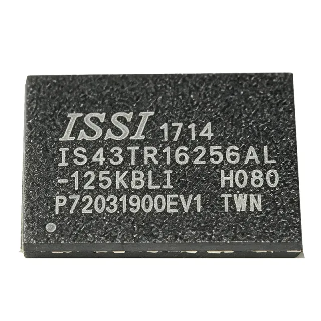
IS43TR16256A-125KBL - 4Gb DDR3 SDRAM 256Mx16 | ISSI
The IS43TR16256A-125KBL is a 4Gbit DDR3 SDRAM organized as 256M x 16, manufactured by Integrated Silicon Solution Inc (ISSI). It operates at a standard voltage of 1.5V (VDD and VDDQ) with a data rate of 1600MT/s (800 MHz clock), and is available in a 96-ball TWBGA (9x13mm) package. This memory IC is designed for high-speed data transfer in computing, networking, and industrial applications. DDR3 SDRAM (Double Data Rate Type 3 Synchronous Dynamic Random-Access Memory) is a type of volatile memory that transfers data on both edges of the clock signal, effectively doubling the data rate compared to DDR2. It is a key component in systems requiring high bandwidth and low latency, such as servers, routers, and embedded processors. DDR3 operates at lower voltages (1.5V or 1.35V for DDR3L) than previous generations, reducing power consumption. Key features include a 4Gbit density, 16-bit I/O width, 800 MHz clock frequency, and a CAS latency of 11 (CL=11) at 1600MT/s. The device supports on-die termination (ODT), programmable CAS latency, and burst lengths of 8 and 4 (with burst chop). It also features auto refresh and self refresh modes for power saving. The 96-ball TWBGA package provides a compact footprint suitable for space-constrained designs. The IS43TR16256A-125KBL uses a high-performance CMOS process and includes a DLL (Delay-Locked Loop) for precise timing alignment. It supports a burst length of 8 with a burst chop of 4, and features programmable read and write latencies. The device also includes a temperature-compensated self-refresh (TCSR) mode to reduce power consumption at high temperatures. Typical applications include main memory for embedded systems, networking equipment (routers, switches), industrial PCs, and high-performance computing modules. Its 1.5V operation and 1600MT/s speed make it suitable for a wide range of DDR3-based designs. When designing with this device, ensure proper decoupling capacitors near the VDD and VDDQ pins, and follow the PCB layout guidelines for DDR3 routing to maintain signal integrity. The device requires a 1.5V supply and a separate VDDQ supply, both with tight tolerance (±0.075V).
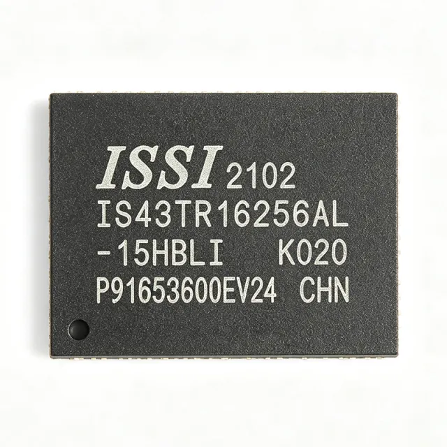
IS43TR16256A-15HBL-TR - 4Gb DDR3 SDRAM 667MHz | ISSI
The IS43TR16256A-15HBL-TR is a 4Gbit DDR3 SDRAM organized as 256M x 16, operating at a clock frequency of 667 MHz (data rate 1333 Mbps) with a CAS latency of 20 ns. It is housed in a 96-ball TWBGA (9x13 mm) package and operates from a 1.5V power supply. This memory IC is designed for high-bandwidth applications requiring reliable, high-speed data storage and retrieval. DDR3 SDRAM (Double Data Rate Type 3 Synchronous Dynamic Random-Access Memory) is a type of synchronous dynamic random-access memory with a high bandwidth interface, double the data rate of DDR2. It achieves higher transfer rates by transferring data on both edges of the clock signal, effectively doubling the data rate without increasing the clock frequency. DDR3 is part of the SDRAM family, which includes DDR, DDR2, DDR4, and DDR5, and is widely used in computing, networking, and embedded systems. Key features include a 4Gbit density, 16-bit I/O organization, 667 MHz clock speed, and a 20 ns CAS latency. The device supports programmable CAS latency, burst lengths of 8 and 4 (with burst chop), and on-die termination (ODT) for improved signal integrity. It also features auto-refresh and self-refresh modes for power saving, and a temperature-compensated self-refresh (TCSR) option. The IS43TR16256A-15HBL-TR utilizes a high-performance CMOS process and a bank architecture with 8 internal banks, enabling efficient interleaving and high throughput. The device includes DLL (Delay-Locked Loop) for precise timing alignment and supports write leveling and read leveling for system timing calibration. Its low power consumption and high speed make it suitable for a wide range of applications. Typical applications include networking equipment (routers, switches), industrial computing, embedded systems, and consumer electronics such as set-top boxes and smart TVs. The 1.5V operation and 96-ball TWBGA package allow for compact PCB designs with good thermal performance. When designing with this device, ensure proper decoupling capacitors near the power pins and follow the layout guidelines in the datasheet to minimize signal integrity issues. The device requires a stable 1.5V supply and a reference voltage (VREF) for the I/O.
IS43TR16256AL-107MBL - 4Gb DDR3L SDRAM 256Mx16 | ISSI
The IS43TR16256AL-107MBL is a 4Gb DDR3L SDRAM organized as 256Mx16, operating at 1.35V with a data rate of 1866MT/s. It is housed in a 96-ball TWBGA (9x13mm) package, offering high density and low power consumption for a wide range of computing and embedded applications. DDR3L (Low Voltage DDR3) is a type of synchronous dynamic random-access memory that operates at 1.35V, reducing power consumption by about 15% compared to standard 1.5V DDR3. It is part of the DDR3 SDRAM family, which uses double data rate architecture to transfer data on both edges of the clock, achieving high bandwidth. DDR3L is commonly used in mobile devices, networking equipment, and industrial computing where power efficiency is critical. Key features include a parallel interface with 933 MHz clock speed, 20 ns access time, and support for 1866MT/s data rate. The device supports various burst lengths (8 and 4 with burst chop), on-die termination (ODT), and programmable CAS latency. It operates over a temperature range of 0°C to +95°C (case) and is RoHS compliant. The IS43TR16256AL-107MBL utilizes advanced DRAM process technology, providing high reliability and performance. It features auto-refresh and self-refresh modes, which are essential for low-power standby operation. The 96-ball TWBGA package ensures excellent thermal and electrical performance, making it suitable for space-constrained designs. Typical applications include networking routers and switches, enterprise storage systems, industrial PCs, and embedded computing platforms. Its low voltage and high density make it ideal for memory-intensive applications where power efficiency is a priority. When designing with this device, ensure proper decoupling capacitors are placed near the power pins to minimize noise. The DDR3L interface requires careful PCB layout to maintain signal integrity at high speeds, including matched trace lengths and controlled impedance.
IS43TR16256AL-107MBLI - 4Gb DDR3L SDRAM 256Mx16 | ISSI
The IS43TR16256AL-107MBLI is a 4Gb DDR3L SDRAM organized as 256M x 16 bits, operating at a clock speed of 933 MHz (data rate 1866 Mbps) with a supply voltage of 1.35V. It is housed in a 96-ball TWBGA (9x13mm) package, making it suitable for high-density memory applications in computing, networking, and industrial systems. DDR3L SDRAM (Double Data Rate 3 Low Voltage) is a type of synchronous dynamic random-access memory that operates at a lower voltage (1.35V) compared to standard DDR3 (1.5V), reducing power consumption by up to 20% while maintaining backward compatibility with 1.5V operation. It is part of the DDR3 memory family, which uses double data rate signaling to transfer data on both edges of the clock, achieving high bandwidth for demanding applications. Key features include a 16-bit I/O interface, 4Gbit density, 20ns access time, and support for 1.35V operation with backward compatibility to 1.5V. The device offers high-speed data transfer rates, low power consumption, and is RoHS compliant. The 96-ball TWBGA package provides a compact footprint suitable for space-constrained designs. Technically, the IS43TR16256AL-107MBLI utilizes a 4-bank architecture with 8 internal banks, supporting burst lengths of 8 and 4, and features on-die termination (ODT) for improved signal integrity. It includes programmable CAS latency, additive latency, and write latency, allowing system designers to optimize timing for their specific memory controller. The device also supports auto-refresh and self-refresh modes for power saving. Typical applications include servers, networking equipment, industrial PCs, and embedded systems where high memory density and low power are critical. The 1.35V operation makes it ideal for power-sensitive designs, while the 1866 Mbps data rate supports high-bandwidth workloads. When designing with this device, ensure proper decoupling capacitors near the power pins and follow the layout guidelines in the datasheet to minimize signal integrity issues. The device requires a stable 1.35V supply and careful attention to termination for the address/control and data lines.
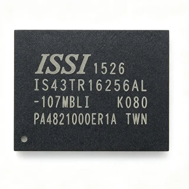
IS43TR16256AL-107MBLI-TR - 4Gb DDR3L SDRAM 256Mx16 | ISSI
The IS43TR16256AL-107MBLI-TR is a 4Gb DDR3L SDRAM organized as 256Mx16, operating at 1.35V with a data rate of 1866 Mbps (933 MHz clock). It is housed in a 96-ball TWBGA (9x13mm) package and is designed for low-power applications requiring high memory density. This device is backward compatible with 1.5V DDR3, allowing flexible system design. DDR3L SDRAM is a type of double data rate synchronous dynamic random-access memory that operates at a lower voltage (1.35V) compared to standard DDR3 (1.5V), reducing power consumption by about 20%. It is part of the memory hierarchy in computing systems, serving as main memory for processors, and is widely used in servers, networking equipment, and embedded systems where power efficiency is critical. Key features include a parallel interface with 16-bit data bus, 20ns access time, and support for on-die termination (ODT) and DLL-off mode for power saving. The device supports burst lengths of 8 and 4, and includes programmable CAS latency and additive latency. It operates over a temperature range of 0°C to +95°C (case temperature) for standard operation. The IS43TR16256AL-107MBLI-TR utilizes advanced DRAM process technology to achieve high density and low power. It features auto-refresh and self-refresh modes, with a typical self-refresh current of [DATA_NEEDED: self-refresh current]. The device includes a mode register set (MRS) for configuration, and supports write leveling and read leveling for signal integrity in high-speed systems. Typical applications include servers, networking equipment, industrial computing, and embedded systems where high memory density and low power are required. The 1.35V operation makes it ideal for battery-powered devices and energy-efficient data centers. When designing with this device, ensure proper decoupling capacitors near the power pins and follow the PCB layout guidelines in the datasheet to maintain signal integrity at 1866 Mbps. The device requires a stable 1.35V supply and a separate VDDQ supply for the I/O.
IS43TR16256AL-125KBL - 4Gb DDR3L SDRAM 256Mx16 | ISSI
The IS43TR16256AL-125KBL is a 4Gbit DDR3L SDRAM organized as 256M x 16, operating from a 1.35V supply with backward compatibility to 1.5V. It is housed in a 96-ball TWBGA (9x13mm) package and supports data rates up to 1600Mbps (800 MHz clock). This memory IC is designed for high-performance computing, networking, and embedded systems requiring low power and high bandwidth. DDR3L (Double Data Rate 3 Low Voltage) is a type of synchronous dynamic random-access memory (SDRAM) that operates at a lower voltage (1.35V) compared to standard DDR3 (1.5V), reducing power consumption by about 20-30% while maintaining similar performance. It is part of the DDR3 family, which uses double data rate signaling to transfer data on both edges of the clock, and is widely used in laptops, servers, and industrial applications where energy efficiency is critical. Key features include a parallel interface with 16-bit data bus, 800 MHz clock frequency, 20 ns access time, and support for 1.35V operation. The device is RoHS compliant and lead-free, making it suitable for environmentally conscious designs. The 96-TWBGA package offers a compact footprint with a 9x13mm body, ideal for space-constrained PCB layouts. Technically, the IS43TR16256AL-125KBL uses a high-density DRAM process, achieving 4Gbit capacity in a single package. It supports standard DDR3L features such as on-die termination (ODT), programmable CAS latency, and burst lengths of 8. The low voltage operation reduces I/O power, while the 20ns access time ensures fast random access for demanding applications. Typical applications include embedded computing, networking equipment (routers, switches), industrial automation, and automotive infotainment systems. Its low power and high density make it ideal for memory-intensive tasks in portable and battery-powered devices. When designing with this component, ensure proper decoupling capacitors near the power pins and follow the layout guidelines in the datasheet to minimize signal integrity issues at high speeds. The 1.35V supply must be regulated accurately to maintain reliable operation.
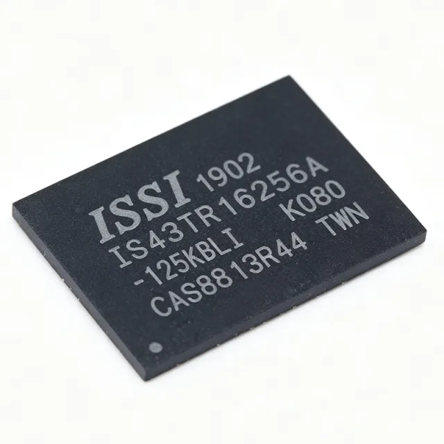
IS43TR16256AL-125KBLI-TR - 4Gbit DDR3L SDRAM 256Mx16 | ISSI
The IS43TR16256AL-125KBLI-TR is a 4Gbit DDR3L SDRAM organized as 256M x 16, operating at a clock frequency of 800 MHz (data rate 1600 Mbps) with a CAS latency of 11. It is supplied in a 96-ball TWBGA (9x13 mm) package and is designed for low-voltage operation at VDD and VDDQ = 1.35V, with backward compatibility to 1.5V. This memory IC is part of ISSI's DDR3L family, offering high density and bandwidth for a wide range of applications. DDR3L (Double Data Rate 3 Low Voltage) SDRAM is a type of synchronous dynamic random-access memory that transfers data on both edges of the clock signal, effectively doubling the data rate. The 'L' designation indicates low-voltage operation at 1.35V, reducing power consumption by about 20% compared to standard DDR3 at 1.5V. DDR3L is widely used in mobile devices, embedded systems, and industrial computing where power efficiency is critical. It is backward compatible with 1.5V DDR3, allowing flexible system design. Key features include a 4Gbit density, 16-bit data bus, 800 MHz clock speed, and a burst length of 8. The device supports on-die termination (ODT), programmable CAS latency, and auto-refresh and self-refresh modes. It operates over a temperature range of -40°C to +95°C (TC), making it suitable for industrial environments. The 96-ball TWBGA package provides a compact footprint with excellent thermal and electrical performance. Technically, the IS43TR16256AL-125KBLI-TR uses a 1.35V power supply for both core and I/O, reducing power dissipation. It features a 20ns row cycle time (tRC) and a 20ns row active time (tRAS). The device supports a data transfer rate of 1600 Mbps per pin, delivering high bandwidth for memory-intensive applications. The low-voltage operation and industrial temperature range make it ideal for embedded systems that require reliable performance in harsh conditions. Typical applications include industrial automation, networking equipment, embedded computing, and automotive infotainment systems. The 4Gbit density and x16 organization are well-suited for applications requiring moderate memory capacity with a wide data bus. The low-voltage operation helps extend battery life in portable devices and reduces thermal load in dense systems. When designing with this component, ensure proper decoupling capacitors are placed near the power pins to minimize noise. The DDR3L interface requires careful PCB layout to maintain signal integrity at 1600 Mbps. Refer to the ISSI datasheet for detailed timing parameters and layout guidelines.
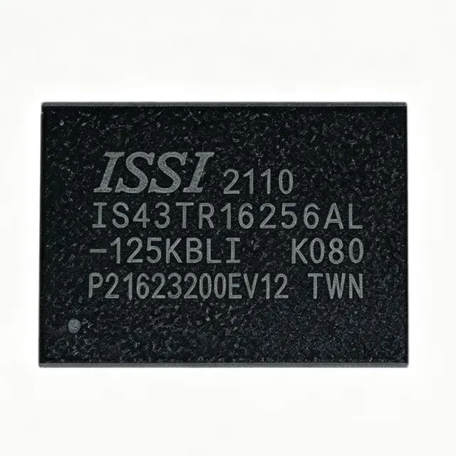
IS46TR16256A-125KBLA2 - 4Gb DDR3 SDRAM 256Mx16 | ISSI
The IS46TR16256A-125KBLA2 is a 4Gb DDR3 SDRAM organized as 256Mx16, operating at 1.5V with a data rate of 1600MT/s (800 MHz clock). It is housed in a 96-ball TWBGA (9x13mm) package, offering high-density memory for computing, networking, and industrial applications. This device supports 8 internal banks for concurrent operation and features programmable CAS latency, burst length, and on-die termination (ODT) for signal integrity. DDR3 SDRAM (Double Data Rate Type 3 Synchronous Dynamic Random-Access Memory) is a type of synchronous dynamic random-access memory with a high bandwidth interface, transferring data on both rising and falling edges of the clock. It is the successor to DDR2 and offers higher speeds and lower power consumption, making it a standard choice for main memory in computers, servers, and embedded systems. DDR3 operates at 1.5V, reducing power compared to DDR2's 1.8V, and supports data rates from 800 to 2133 MT/s. Key features include a 20ns tRCD (RAS-to-CAS delay), 290mA operating current, and a temperature range of 0°C to +95°C (Tc). The device is RoHS compliant and supports both standard and low-voltage (1.35V) operation, providing flexibility in power-sensitive designs. The 96-ball TWBGA package with a 9x13mm footprint enables compact PCB layouts, and the 256Mx16 organization simplifies bus design by reducing the number of devices needed for wide data paths. Architecturally, the IS46TR16256A-125KBLA2 uses an 8-bank design with a 16-bit I/O interface, achieving a peak bandwidth of 12.8 GB/s per device. It incorporates DLL (Delay-Locked Loop) for precise clock alignment, and supports programmable read and write latencies. The device also features auto-refresh and self-refresh modes for power management, and on-die termination (ODT) to improve signal quality on high-speed buses. Typical applications include main memory for embedded processors, networking equipment (routers, switches), industrial PCs, and high-performance computing modules. Its high density and speed make it suitable for applications requiring large memory footprints, such as video processing, data acquisition, and telecommunications infrastructure. When designing with this DDR3 device, ensure proper termination and layout for high-speed signals, and follow the JEDEC DDR3 guidelines for power supply decoupling and signal integrity. The device requires a 1.5V supply for VDD and VDDQ, and a separate VREF for address/command signals.

IS61C6416AL-12TLI - 1Mb 64Kx16 12ns Async SRAM | ISSI
The Integrated Silicon Solution Inc (ISSI) IS61C6416AL-12TLI is a 1 Mbit high-speed asynchronous CMOS Static RAM organized as 65,536 words by 16 bits, with 12 ns access time, housed in a 44-pin TSOP Type II industrial-grade package. It operates from a single 4.5 V to 5.5 V supply and provides a 16-bit parallel I/O bus, making it well suited as cache, buffer, or scratchpad memory in 16-bit and 32-bit embedded systems. What is an asynchronous SRAM? An asynchronous SRAM (Static Random-Access Memory) is a volatile memory device whose read and write cycles are triggered directly by address and control-line transitions, with no external clock required. It sits in the computer-memory hierarchy above DRAM in speed and below on-chip cache in density, and is commonly chosen when deterministic, low-latency random access (single-digit to a few tens of nanoseconds) matters more than density or cost-per-bit. Within ISSI's portfolio it belongs to the IS61C6416AL family of 64Kx16 high-speed CMOS SRAMs. Key features of the IS61C6416AL-12TLI include 12 ns typical access time, low-power CMOS operation with CMOS- and TTL-compatible I/O, automatic power-down when deselected, and separate upper-byte (UB) and lower-byte (LB) enables for byte-wide writes. The 44-pin TSOP-II footprint is JEDEC-standard, simplifying PCB layout and second-sourcing. The industrial temperature grade (-40C to +85C) supports harsh-environment deployment. The device is fabricated using ISSI's high-performance CMOS process, yielding an access time of 12 ns while keeping active and standby currents low. Data is retained as long as power is applied, with no refresh cycles. The active-low write enable (WE#) and chip-enable (CE#) signals give the designer full read/write control, and the byte-control pins (UB#, LB#) allow efficient use of the 16-bit data bus in mixed-width systems. Typical applications include networking line cards, industrial control and instrumentation, automotive infotainment subsystems, telecom routers and switches, RAID controllers, set-top boxes, and any 16-bit or 32-bit embedded CPU system that needs a fast external memory for buffers, FIFOs, or lookup tables. The TSOP-II package and standard JEDEC pinout also make it a popular choice for legacy designs that must be maintained or refreshed. When designing with this part, observe the standard SRAM power-supply decoupling practice: place a 0.1 uF ceramic bypass capacitor as close as possible to the VCC and VSS pins. Unused inputs (UB#, LB#, WE#) should be tied to VCC through a pull-up to prevent unwanted writes. Designers should also note that the asynchronous interface means there is no clock-domain crossing required when interfacing to legacy microcontrollers or DSPs that lack an external memory controller with SRAM timing support. This page synthesizes distributor pricing, parametric drop-in alternatives, and practical design notes that are not gathered in the manufacturer datasheet alone, giving engineers a single source for sourcing, replacement, and PCB-layout decisions.

IS61WV102416DBLL-10TLI - 16Mb Async SRAM 1Mx16 10ns | ISSI
The ISSI IS61WV102416DBLL-10TLI is a 16-Mbit high-speed asynchronous CMOS static RAM organized as 1M words by 16 bits, housed in a 48-pin TSOP-I package. According to the ISSI datasheet for the IS61/64WV102416DALL/BLL family, the device operates from a single 2.4V to 3.6V supply (with 3.3V nominal) and provides a 10 ns access time, making it suitable for high-performance memory subsystems where deterministic, low-latency read/write cycles are required without the complexity of a DRAM controller. The 'D' prefix designates the lower-voltage 2.4V-3.6V variant, while the 'BLL' suffix indicates the specific speed grade and package option. Asynchronous static RAM (SRAM) is a volatile memory technology that retains data as long as power is applied, without the refresh cycles required by DRAM. Within the broader memory hierarchy, SRAM sits closest to the processor because of its sub-15 ns access times; it is used for cache, look-up tables, scratch-pad buffers, and FIFO storage in networking, industrial, and embedded systems. Compared with synchronous SRAM (such as QDR or DDR SRAM), asynchronous SRAM uses simple chip-enable, output-enable, and write-enable control signals and is ideal for glue-less processor bus interfaces. The IS61WV102416DBLL-10TLI provides fully static operation (no clock required), TTL-compatible I/O levels, common data-in/data-out bus architecture, and an active-low output enable for bus sharing. Power consumption is minimized through a Chip Enable power-down mode, and the device supports industrial temperature range operation. The CMOS fabrication process delivers high noise immunity and low standby current, both of which are critical for battery-backed or energy-conscious designs. Typical applications include industrial controllers, networking line cards, routers and switches requiring fast look-up tables, automotive telematics (non-safety-critical subsystems), medical instrumentation buffers, RAID controllers, and any embedded CPU/MCU design that needs a large, low-latency external data store beyond the on-chip SRAM budget. The wide word width (x16) is well matched to 16-bit and 32-bit microcontrollers and DSPs. When designing with this device, keep in mind that asynchronous SRAM bandwidth is limited by the controller's ability to issue back-to-back read or write strobes, so the 10 ns access time implies roughly 100 MHz equivalent single-transfer throughput per cycle. Decoupling and signal routing must be handled carefully on long busloads to maximize margin. This page synthesizes distributor pricing, drop-in alternative cross-references, and practical design notes that go beyond the manufacturer datasheet to help engineers evaluate and qualify the part quickly.

JS28F320J3F75A - 32Mbit Parallel NOR Flash, 75ns, 56-TSOP | Micron
The Micron JS28F320J3F75A is a 32-Mbit (4M x 8 / 2M x 16) parallel NOR flash memory device with a 75 ns initial access time, operating from a 2.7 V to 3.6 V single supply, and housed in a 56-pin Thin Small Outline Package (TSOP Type I). It belongs to the J3 family of embedded flash memories built on 65 nm Single Bit per Cell (SBC) technology, providing reliable non-volatile code and data storage for embedded systems. A parallel NOR flash is a non-volatile memory type that supports random read access (execute-in-place / XIP), byte-level program, and sector erase operations. Within the memory hierarchy, NOR flash sits between SRAM (volatile, fastest) and NAND flash (non-volatile, higher density, sequential access). NOR is preferred when a microprocessor needs to fetch code directly from the array without first copying to RAM, and when reliable long-term data retention with low software complexity is required. Key features include symmetric 128-Kbyte uniform blocks (parameter blocks) or 64-Kword blocks, top or bottom boot block configurations, hardware write protection, a deep power-down mode for low standby current, and command-set compatibility with the Common Flash Interface (CFI). The device supports 100,000 program/erase cycles per block and a minimum 20-year data retention. Its 75 ns access time makes it suitable for microprocessors and ASICs operating at bus frequencies up to approximately 50 MHz without wait states, or higher with proper handshaking. Typical applications include set-top boxes, networking equipment, industrial controllers, automotive infotainment, printers, and any embedded design requiring execute-in-place boot storage. The 56-TSOP footprint is widely supported on legacy and new PCBs, simplifying hardware integration. When designing with this device, ensure the host microcontroller supplies a clean 3.3 V rail within the 2.7 V-3.6 V tolerance, and respect the program/erase timing budget. Adding a 0.1 uF decoupling capacitor close to VCC and VCCQ pins is recommended for reliable operation across temperature. This page synthesizes distributor pricing, drop-in alternatives, and practical design notes not found in the manufacturer datasheet alone. All values are referenced to current Micron datasheet and live distributor inventory as of 2026-10-05.
K3K8K80BM-JGCT - Samsung LPDDR DRAM Memory IC | Samsung Electronics
The Samsung Electronics K3K8K80BM-JGCT is a mobile DRAM memory IC from Samsung's K3K series of low-power SDRAM components, supplied in a ball grid array (BGA) package for space-constrained mobile and embedded designs. Samsung's K3K part-number prefix designates its LPDDR (Low Power Double Data Rate) DRAM component family used in smartphones, tablets, and embedded computing platforms. Low-power DDR DRAM is a class of volatile memory that transfers data on both edges of the clock to double bandwidth while reducing operating and standby power. Within the memory hierarchy, LPDDR sits below DDR5 server DIMMs in raw bandwidth but dominates mobile and battery-powered systems because of its low core voltage, deep power-down modes, and PoP (Package-on-Package) or discrete BGA mounting options. It is a direct child of the broader SDRAM/DRAM semiconductor category. Key characteristics of this device class include high-speed bidirectional data transfer, per-bank and per-rank power management, dynamic voltage and frequency scaling, and initialization/training sequences defined by the JEDEC LPDDR specification in force for the die generation. Samsung mass-produces these dies on advanced DRAM process nodes with stacked or planar cell arrays. Architecturally, Samsung LPDDR components integrate the memory array, sense amplifiers, row/column decoders, DLL/phase-alignment circuitry, and I/O gating on a single die, with the package ball map exposing the CA (command/address) bus and DQ data lanes. Typical applications include smartphone application-processor memory, tablet and notebook SoC main memory, automotive infotainment memory subsystems, and embedded AI/edge-computing modules that require high bandwidth per watt. A key design consideration is signal integrity: LPDDR CA/DQ routing requires length-matched, impedance-controlled traces and careful fly-by or daisy-chain topology, and controller training must match the Samsung die's datasheet timing parameters. This page synthesizes verified distributor data, same-family alternative MPNs, and practical design notes not found in the manufacturer datasheet.
K3K9K90BM-MGCP - LPDDR5 DRAM | Samsung Semiconductor
The Samsung K3K9K90BM-MGCP is an LPDDR5 (Low Power Double Data Rate 5) DRAM memory integrated circuit from Samsung Semiconductor, supplied in a PBGA (Plastic Ball Grid Array) package. Samsung's LPDDR5 family delivers pin speeds of up to 6400 Mbps and aggregate bandwidth of up to 51.2 GB/s per device, with approximately 20% lower power consumption than the previous LPDDR4X generation. LPDDR5 DRAM is a type of synchronous dynamic random-access memory optimized for low power and high bandwidth in mobile, edge computing, and embedded systems. In the memory hierarchy it sits under the DRAM -> synchronous DRAM -> low-power SDRAM taxonomy defined around the JEDEC LPDDR5 standard, and it succeeds LPDDR4X in mobile SoC memory subsystems. Key features of Samsung LPDDR5 devices include 6400 Mbps pin speed, deep power-down and per-bank refresh architectures that cut idle power, and a simplified two-channel architecture that improves command efficiency versus LPDDR4X. Density options across the K3K/K3L family range from 32 Gbit to 64 Gbit per package, organized as x32-wide interfaces for SoC attachment. Technically, LPDDR5 introduces WCK (word clock) strobing, bank group architecture, and DVFS (dynamic voltage frequency scaling) of the clock domain, allowing the memory controller to throttle speed and voltage to match workload, which is the main source of the ~20% system power saving versus LPDDR4X. Typical applications include flagship smartphone and tablet main memory, AI edge accelerators, automotive infotainment and ADAS platforms, and 5G networking equipment where high bandwidth per watt is critical. Design consideration: LPDDR5 signal integrity requires tightly matched length routing of CA, DQ, DQS, and WCK traces on the PCB; consult the Samsung LPDDR5 design guide for fly-by topology and termination recommendations. This page synthesizes distributor stock data, drop-in same-family alternatives, and practical design notes not found in the manufacturer datasheet.
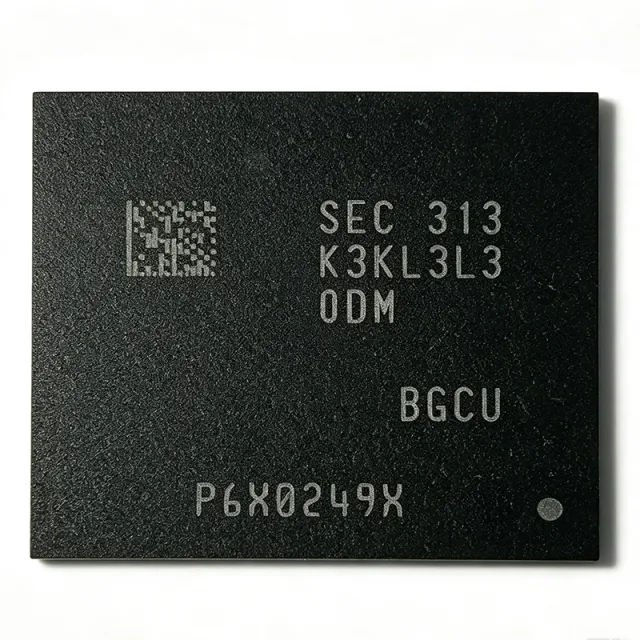
K3KL3L30DM-BGCU - LPDDR5X 64Gb 8533Mbps DRAM | Samsung
The Samsung Semiconductor K3KL3L30DM-BGCU is a 64 Gb LPDDR5X low-power DRAM memory IC operating at 8533 Mbps data rate, organized x64, in a 496-ball FBGA package. It operates from multiple supply rails of 1.8 V, 1.05 V, 0.9 V and 0.5 V and is rated for -25 C to +85 C operation. LPDDR (Low Power Double Data Rate) SDRAM is a type of synchronous dynamic random-access memory optimized for mobile and power-sensitive systems. Within the memory hierarchy, LPDDR5X sits at the top of the JEDEC low-power DRAM family (LPDDR4 -> LPDDR5 -> LPDDR5X), functioning as the main-system memory IC that feeds CPUs, GPUs and NPUs in smartphones, tablets, automotive computing platforms and AI edge devices. Key features of the K3KL3L30DM-BGCU include its 8533 Mbps pin speed, which places it in the highest LPDDR5X speed bin, and its 64 Gb density per device, enabling multi-gigabyte system memory with only a few ICs. The x64 organization and 496-ball FBGA footprint allow dense PCB routing on mobile-style boards. Technically, LPDDR5X extends LPDDR5 with higher signaling rates and improved power efficiency. Samsung states its LPDDR5X family delivers up to 8.5 Gbps data processing speeds with approximately 20% better power efficiency than LPDDR5, making it suited to AI inference, high-resolution imaging pipelines and 5G data throughput. Typical applications include flagship smartphone main memory, automotive infotainment and ADAS compute modules, AI edge accelerators, and premium tablet and laptop DRAM subsystems paired with Qualcomm or MediaTek application processors. A key design consideration is power-integrity: LPDDR5X at 8533 Mbps demands tight rail regulation on the 0.5 V VDDQ domain, careful fly-by trace length matching and per-rail decoupling per the memory controller vendor layout guide. This page consolidates distributor stock signals, family cross-references and practical sourcing notes beyond the bare datasheet listing. Pricing is RFQ-based as of 2026-09-04 because this EOL-status part trades through broker channels rather than fixed catalog tiers.
K3KL3L30QM-JGCT - LPDDR5X 64Gb 7500Mbps DRAM | Samsung
The Samsung K3KL3L30QM-JGCT is a 64 Gb LPDDR5X DRAM memory IC organized x64, supporting data rates up to 7500 Mbps per pin, supplied in a fine-pitch ball grid array (FBGA) package for mobile and edge computing platforms. LPDDR5X (Low Power Double Data Rate 5X, per the JEDEC LPDDR5X standard family) is an extension of LPDDR5 that raises signaling speed and improves power efficiency for battery-operated and thermally constrained systems. In the memory hierarchy it sits as volatile main-system DRAM below persistent storage such as NAND flash and eMMC, providing the working memory bandwidth that CPUs, GPUs, and NPUs require. Key features of the K3KL3L30QM-JGCT include its 64 Gbit density (8 GB equivalent per device), x64 organization for wide memory buses, and 7500 Mbps/pin data rate, which places it in the LPDDR5X performance tier used by flagship smartphones, tablets, AI edge accelerators, and automotive infotainment SoCs. As a Samsung third-generation 10nm-class DRAM product line part, it delivers higher bandwidth than LPDDR5 at lower power per transferred bit. Technically, LPDDR5X operates with a low-voltage I/O rail (VDDQ around 0.3-0.5 V class, per Samsung LPDDR5X documentation) and uses advanced training, on-die termination, and link ECC-style features inherited from LPDDR5 to maintain signal integrity at multi-gigabit speeds. Ball-grid-array interconnects minimize parasitic inductance, enabling clean eye diagrams at 7500 Mbps when the PCB stackup follows Samsung's package-on-package and fly-by routing guidance. Typical applications include flagship smartphone and tablet main memory, AI accelerator and NPU buffer memory, automotive domain-controller DRAM, and high-performance embedded and edge-server modules such as LPDDR5X SODIMMs and memory-down designs. Design consideration: LPDDR5X signal integrity is highly layout sensitive - length-matched, reference-plane-continuous routing and strict power-integrity budgeting for VDDQ are mandatory; insufficient decoupling at 7500 Mbps manifests as training failures rather than gradual degradation. This page adds value beyond the datasheet by synthesizing distributor stock levels, drop-in family alternatives, and practical design notes in one place.
K3KL5L50DM-BGCU - LPDDR5X 128Gb 8533Mbps DRAM | Samsung
The Samsung Semiconductor K3KL5L50DM-BGCU is a premium low-power DRAM (LPDDR5X) memory IC offering 128 Gb (16 GB) of density and an 8533 Mbps data rate per pin, packaged in a fine-pitch ball grid array (496-ball FBGA per distributor listings). It belongs to Samsung's LPDDR5X family, which delivers up to 8.5 Gbps pin speeds and approximately 20% better power efficiency than LPDDR5 at comparable speeds. LPDDR5X (Low Power Double Data Rate 5X) is an JEDEC-defined evolutionary step of the LPDDR5 SDRAM standard, aimed at mobile, automotive, and edge-AI computing systems. In the memory hierarchy, DRAM sits as the main system memory between the processor and non-volatile storage, providing high-bandwidth working memory; LPDDR variants optimize this role for battery-powered and thermally constrained devices by lowering I/O and core voltages and adding deep power-down states. Key characteristics of this part include the 128 Gb monolithic density, the 8533 Mbps (8.5 Gbps) transfer rate per data pin, and the ultra-low-power architecture typical of Samsung's LPDDR5X portfolio, which supports dynamic voltage scaling and advanced sleep modes. The high pin speed translates directly into memory bandwidth critical for large-language-model inference, 5G modems, and high-resolution imaging pipelines. Technically, LPDDR5X devices use bank group architectures with 16n prefetch, on-die termination, and command/address training to sustain multi-gigabit signaling. Samsung's premium LPDDR5X line further emphasizes power efficiency through enhanced ECC features and refined process nodes, allowing smartphone SoCs and automotive ADAS platforms to exploit full bandwidth within tight thermal envelopes. Typical applications include flagship smartphone and tablet main memory (often stacked as multi-die packages), AI accelerator companion memory in edge servers, automotive infotainment and ADAS domains, and high-performance embedded modules. A key design consideration: LPDDR5X signal integrity at 8.5 Gbps demands strict fly-by topology routing, length-matched traces, and SoC memory-controller training support; dropping to an LPDDR5-only controller limits operation to 6400 Mbps class speeds. This page synthesizes distributor stock data (16,750 pcs reported as of Aug 31, 2026), same-family alternatives, and practical design notes not found in the manufacturer datasheet.

K3KL5L50QM-JGCT - 128Gb LPDDR5X 7500Mbps DRAM | Samsung
The Samsung K3KL5L50QM-JGCT is a 128 Gb (16 GB) LPDDR5X low-power DRAM memory IC delivering data rates up to 7500 Mbps per pin with a x64 organization, housed in a 441-ball FBGA package operating from -25C to +85C across 1.8 V, 1.05 V, 0.9 V and 0.5 V supply domains. LPDDR5X (Low Power Double Data Rate 5X eXtended) is an enhanced evolution of the LPDDR5 DRAM standard defined by JEDEC. As a class of volatile DRAM within the broader memory hierarchy (LPDDR5X -> LPDDR family -> DRAM -> semiconductor memory), it prioritizes bandwidth-per-watt for battery-powered and thermally constrained compute platforms. Compared with LPDDR5, LPDDR5X raises interface speed and improves power efficiency, making it the dominant main-memory technology for flagship smartphones, tablets, and increasingly for AI accelerators and automotive computing. Key features of the K3KL5L50QM-JGCT include its 128 Gb monolithic density in a compact 441-ball FBGA footprint, 7500 Mbps (LPDDR5X-7500) interface speed, x64 channel organization suitable for 16-bit channel stacking, and an industrial-extended -25C to +85C operating range. Samsung reports that its premium LPDDR5X generation delivers up to 1.25 times the speed and roughly 25% better power efficiency versus the previous generation. Technically, the device uses Samsung advanced DRAM process technology with a multi-rail power architecture: VDD1 (1.8 V), VDD2 (1.05 V), VDDQ (0.5 V) and VDDCA/other aux rails, minimizing I/O switching power at multi-gigabit rates. The x64 organization allows SoC memory controllers to aggregate two 32-bit channels for full-bandwidth LPDDR5X operation. Typical applications include flagship smartphone and tablet main memory, AI edge computing and inference accelerators, in-vehicle infotainment and ADAS compute modules, and high-performance ultra-thin PCs. Design consideration: because this part is a ball-grid array memory, signal integrity on the command/address and data buses is critical; follow the SoC vendor reference layout for fly-by routing, ODT settings, and power rail sequencing. This page synthesizes distributor stock, drop-in family alternatives, and practical design notes not found in the manufacturer datasheet.

K3KL7L70EM-MGCU - 12Gb LPDDR5X DRAM, 315-Ball FBGA | Samsung
The Samsung K3KL7L70EM-MGCU is a 12 Gigabit (12 Gb) LPDDR5X low-power synchronous DRAM memory chip from Samsung Semiconductor, supplied in a 315-ball FBGA (Fine-Pitch Ball Grid Array) surface-mount package. This LPDDR5X DRAM is engineered for bandwidth-intensive, power-sensitive mobile and edge-computing platforms, operating at a data rate of up to approximately 8533 Mbps/pin as offered in Samsung's LPDDR5X family. LPDDR5X (Low Power Double Data Rate 5X eXtended) is an evolution of the LPDDR5 memory standard defined by JEDEC, pushing data rates and energy efficiency beyond conventional LPDDR5. In the memory hierarchy, DRAM sits between on-chip SRAM caches and non-volatile storage such as NAND flash, serving as the main working memory of a system-on-chip (SoC). LPDDR5X specifically targets flagship smartphones, tablets, AI edge accelerators, automotive infotainment, and high-performance portable devices that need more bandwidth than LPDDR5 at comparable or lower power. Key features of the K3KL7L70EM-MGCU include its 12 Gb single-die density, LPDDR5X-class speed grading (suffix -MGCU denotes speed and package options per Samsung part numbering), the compact 315-ball FBGA footprint, and Samsung's advanced low-voltage VDDQ operation that reduces I/O power versus LPDDR5. Samsung's LPDDR5X process technology supports deep power-down, per-bank refresh, and advanced bank-group architectures that improve effective bandwidth and standby efficiency. Architecturally, the device is organized as a x32-class LPDDR5X SDRAM with bank groups supporting burst-access scheduling. Command/address and data signals use Samsung LPDDR5X signaling with on-die termination (ODT) and link error checking options implemented per JEDEC LPDDR5X conventions, simplifying SoC PHY integration for Qualcomm Snapdragon and MediaTek Dimensity class platforms. Typical applications include flagship smartphone main memory, AI inference accelerators at the edge, automotive cockpit and ADAS domain controllers, and ultra-thin tablets or laptops using stacked/package-on-package memory configurations. When designing this device in, ensure the SoC memory controller explicitly supports LPDDR5X timing and speed-bin compatibility, and follow Samsung's layout guidelines for fly-by routing of CA/CLK nets and matched-length DQ/DBI/DQS groups. This page consolidates verified distributor listings, drop-in family alternatives, and practical design guidance not found in a single manufacturer datasheet.
K3KL9L90CM-MGCT - 64Gb LPDDR5X 7500Mbps x32 DRAM | Samsung
The Samsung K3KL9L90CM-MGCT is a 64 Gbit LPDDR5X SDRAM with a x32 memory organization and a maximum data rate of 7500 Mbps, housed in a 315-ball FBGA (BGA-315) package. LPDDR5X (Low Power Double Data Rate 5X) is an enhanced evolution of the LPDDR5 standard defined by JEDEC, targeting dramatically higher bandwidth with lower operating voltage. It sits at the top of the mobile DRAM hierarchy (LPDDR4X -> LPDDR5 -> LPDDR5X) and serves as the main-system-memory technology for smartphones, tablets, laptops, AI accelerators, and automotive infotainment platforms. As volatile memory, it provides fast working storage for a processor but must be re-initialized at every power cycle. Key features of this device include the 64 Gbit density per die (8 GByte per package in x32 organization), 7500 Mbps pin speed for approximately 300 Gbps of aggregate bandwidth per 32-bit channel, and LPDDR5X-class low supply voltages (VDDQ 500 mV core interface domain with 900 mV/1.05 V core rails and 1.8 V I/O and power domains per the JLCPCB listing). The industrial-grade operating range of -25C to +85C supports demanding embedded deployments. Architecturally, the device implements LPDDR5X signaling with dynamic voltage scaling, deep sleep modes, and per-bank refresh schemes inherited from LPDDR5, enabling platforms compliant with JEDEC JESD209-5B-class requirements to exploit full 7500 Mbps operation. Command/address training and DFE-based receiver equalization sustain signal integrity at high data rates over standard PCB stackups. Typical applications include AI edge-compute modules, high-performance smartphone and tablet main memory, industrial controllers requiring embedded logging, computing/COM express modules, and firmware boot and data-storage subsystems that pair DRAM with NAND. Design consideration: LPDDR5X at 7500 Mbps requires strict fly-by termination topology, length-matched routing, and careful power-domain isolation of the 500 mV VDDQ rail; memory-controller training quality directly determines achievable speed bin. This page consolidates verified distributor stock, drop-in same-family alternatives, and practical sourcing guidance not found in the manufacturer datasheet.
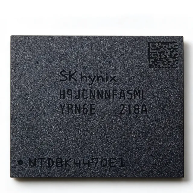
K3LKBKB0BM-MGCP - 32Gbit LPDDR5 DRAM 6400Mbps | Samsung
The Samsung K3LKBKB0BM-MGCP is a 32 Gbit LPDDR5 SDRAM memory IC with a 1G x32 organization and a data rate of 6400 Mbps, operating from 500 mV, 900 mV, 1.05 V and 1.8 V supply rails over an industrial-extended temperature range of -25C to +85C. The device is packaged in a fine-pitch FBGA ball grid array (data indicates FBGA-315, 1.05 V core class) and is RoHS compliant. LPDDR5 (Low Power Double Data Rate 5) is the fifth generation of JEDEC low-power synchronous DRAM, a class of volatile memory that stores working data for application processors and SoCs. Within the memory hierarchy, LPDDR5 sits under the broader DRAM family alongside DDR4/DDR5, but is optimized for bandwidth-per-watt in battery-powered and thermally constrained systems rather than raw module capacity. Key differentiating specifications include the 6400 Mbps/pin data rate, which doubles effective LPDDR4X-class bandwidth in comparable channel conditions; a 32 Gbit single-die density that allows 4 GB of memory in one package with a x32 I/O interface; and multi-rail operation (VDD1 1.05 V class core, VDD2 0.9 V class, VDDQ 0.5 V class, VDD2H 1.8 V class per the distributor listing) that reduces dynamic and standby power. The -25C to +85C operating window extends beyond the standard mobile range, supporting industrial controllers and outdoor connected devices. Technically, the device belongs to Samsung's LPDDR5 family, which uses deep-sleep states, bank-group architecture, and dynamic voltage frequency scaling to cut idle power dramatically versus LPDDR4. Speed-class grading (this part is listed alongside LPDDR5-5500/6400 class material in web listings) allows platform designers to match memory bandwidth to SoC controller capability. Signal integrity at 6400 Mbps requires careful length-matched routing and reference-plane discipline on the PCB. Typical applications include flagship smartphones and tablets, AI edge-compute modules, automotive infotainment SoCs, networking appliances, and industrial computing modules where 4 GB LPDDR5 density and low standby power are required. Design consideration: at 6400 Mbps, routing and power-delivery design dominate system margins; use fly-by topology guidance from the Samsung LPDDR5 datasheet and validate the design at the corner data rates during SI/PI sign-off. This page synthesizes distributor pricing, stock availability, drop-in alternative guidance, and practical design notes not found in the manufacturer datasheet alone.