MOSFET-транзисторы
Товары (1294)

STS5DNF60L - Dual N-Ch 60V 5A 35mΩ STripFET II MOSFET | STMicroelectronics
The STMicroelectronics STS5DNF60L is an automotive-grade dual N-channel 60 V, 35 mΩ typical on-resistance, 5 A STripFET II Power MOSFET housed in an SO-8 surface-mount package. It integrates two independent N-channel MOSFETs in a single 8-pin SOIC outline, making it well suited for half-bridge, full-bridge, and synchronous-rectifier topologies where PCB real estate is constrained. The device is specified for 60 V drain-to-source breakdown, 5 A continuous drain current per channel at 25 °C, and a typical R_DS(on) of 35 mΩ at V_GS = 10 V. A power MOSFET is a voltage-controlled semiconductor switch that uses a gate field to modulate current flow between drain and source terminals. The STripFET II process employed in the STS5DNF60L is specifically engineered to minimize input capacitance and gate charge, which sit inside the broader technology hierarchy of trench MOSFET -> power MOSFET -> discrete semiconductor -> active electronic component. Low Q_g directly reduces driver losses in high-frequency switching applications and enables operation from low-current logic-level gate drivers. Key features include 60 V V_DSS rating, 5 A continuous drain current per channel, 35 mΩ typical R_DS(on) at V_GS = 10 V, low threshold voltage compatible with 3.3 V / 5 V gate drive, low gate charge for fast switching edges, and 100 % avalanche-tested internal construction. The SO-8 footprint provides a standardized land pattern that simplifies automated SMT assembly and supports dual-sided cooling through copper-pour design. From an architecture standpoint, the dual-die monolithic integration shares a common substrate while keeping source pins electrically isolated, so each transistor can be driven independently in any switching configuration. The STripFET II cell geometry lowers conduction losses versus earlier STripFET generations, improving efficiency in DC-DC converter primary-side switches and secondary-side synchronous rectifiers. Typical turn-on delay times are in the tens of nanoseconds, enabling use at switching frequencies from 100 kHz up to several hundred kHz. Typical applications include isolated DC-DC converter primary switches for telecom and computer power supplies, secondary-side synchronous rectification in buck converters, motor-driver half-bridges for low-power BLDC drivers, and automotive 12 V/24 V load switches. The 60 V rating provides ample headroom above 24 V industrial bus rails and 12 V automotive transient excursions. When designing with this part, ensure that gate-drive voltage remains at or above 4.5 V for full enhancement at low temperatures, place the gate-drive resistor within 5 mm of the gate pin to suppress ringing, and keep high-dV/dt loops compact to limit EMI. A low-ESR ceramic bypass of at least 10 µF should sit adjacent to each drain pin for hard-switched topologies. This page synthesizes real distributor stock data, parametric comparison versus alternates, and practical PCB-layout guidance that goes beyond what the manufacturer datasheet alone provides.
STS7DNH3LL - Dual N-Channel 30V MOSFET, 0.018Ω, 7A | STMicroelectronics
The STMicroelectronics STS7DNH3LL is a dual N-channel 30 V STripFET III Power MOSFET array housed in an SO-8 surface-mount package, with a typical on-resistance of 0.018 Ω and per-channel continuous drain current rated up to 7 A. The device integrates two low-RDS(on) N-channel FETs in a single 8-pin SOIC, designed for high-efficiency synchronous rectification and load switching in compact power designs. Its 30 V drain-to-source breakdown and 0.018 Ω RDS(on) at 10 V VGS make it well suited to synchronous buck converters, low-voltage motor drives, and battery protection circuits. A Power MOSFET is a voltage-controlled semiconductor switch that uses an electric field at the gate to control current flow between drain and source, enabling high-efficiency power conversion at switching frequencies that mechanical or bipolar devices cannot achieve. Within the broader semiconductor taxonomy, a Power MOSFET belongs to the discrete transistor family (transistor -> discrete semiconductor -> semiconductor), with the sub-class of enhancement-mode N-channel devices dominating low-voltage synchronous-rectifier designs because N-channel carriers exhibit roughly three times higher mobility than P-channel carriers, lowering conduction loss for a given silicon area. Key features of the STS7DNH3LL include 0.018 Ω typical on-resistance at VGS = 10 V, 30 V VDS max rating, ±20 V VGS rating, low gate charge optimized for STripFET III generation, and an integrated dual-FET topology that halves board area versus two discrete DPAK devices. The SO-8 package supports a maximum power dissipation of approximately 2.5 W per channel with proper copper thermal management, and the device is rated for operation across -55°C to +175°C junction temperature for harsh-environment industrial loads. Architecturally, the STS7DNH3LL uses STMicroelectronics' third-generation STripFET III trench-gate process, which reduces the figure-of-merit RDS(on) × Qg compared to earlier planar generations. This directly translates into lower switching and conduction losses in high-frequency buck and synchronous-rectifier applications. The integrated monolithic dual-die construction also reduces parasitic source inductance relative to discrete pairs, which improves switching performance and reduces ringing on the gate drive waveform. Typical applications include synchronous rectification in 12 V buck converters for telecom and server point-of-load rails, low-voltage DC motor control in robotics and drones, OR-ing and hot-swap circuits on multi-rail backplanes, and high-efficiency battery management in portable electronics and e-bike motor controllers. The dual-FET topology is particularly valuable where PCB real estate is at a premium. When designing with this device, place the gate-drive return paths directly over the source pad to minimize parasitic inductance, and ensure the gate drive voltage is sequenced properly to prevent simultaneous turn-on of both channels. The SO-8 thermal pad is the drain terminal for both FETs, so the PCB copper pour doubles as both a thermal dissipation path and a low-impedance drain connection.

STU16N65M5 - 650V N-Channel Power MOSFET | STMicroelectronics
The STU16N65M5 is an N-channel Power MOSFET from STMicroelectronics, part of the MDmesh M5 series, designed for high-efficiency power conversion applications. It features a breakdown voltage of 650V and a continuous drain current of 16A at 25°C, with a low on-resistance of 0.29 ohm (typical) to minimize conduction losses. The device is housed in an IPAK (TO-251) package, which offers a compact footprint with a metal tab for thermal dissipation, suitable for through-hole mounting in power supplies and industrial equipment. A Power MOSFET is a type of field-effect transistor optimized for switching and amplification of power. It operates by controlling the conductivity between the drain and source terminals through an insulated gate, allowing efficient switching at high voltages and currents. Power MOSFETs are fundamental building blocks in power electronics, serving as switches in DC-DC converters, AC-DC power supplies, motor drives, and lighting systems. They are part of the broader category of discrete semiconductors, which also includes diodes, thyristors, and IGBTs, each tailored for specific power handling and switching requirements. Key features of the STU16N65M5 include a very low gate charge (Qg) of 38 nC (typical), which enables fast switching and reduces driver losses, and a high dv/dt capability for robust performance in hard-switching topologies. The device also offers a wide operating junction temperature range from -55°C to +150°C, ensuring reliability in harsh environments. Its avalanche ruggedness is rated at 400 mJ (single pulse), making it suitable for applications where inductive loads may cause voltage spikes. Technically, the MDmesh M5 series utilizes a proprietary strip layout technology that reduces on-resistance and gate charge simultaneously, achieving a figure of merit (RDS(on) x Qg) that is among the best in its class. This technology enhances the device's efficiency in high-frequency switching applications, where both conduction and switching losses are critical. The STU16N65M5 also features a built-in diode with fast recovery characteristics, reducing reverse recovery losses in bridge topologies. Typical applications include switch-mode power supplies (SMPS) for consumer and industrial electronics, power factor correction (PFC) circuits, LED lighting drivers, and solar inverters. Its 650V rating provides ample margin for universal input (85-265V AC) power supplies, while the low on-resistance ensures high efficiency in continuous conduction mode. When designing with the STU16N65M5, ensure proper gate drive voltage (typically 10V) to fully enhance the channel and minimize on-resistance. A gate resistor may be needed to control switching speed and reduce EMI. Thermal management is crucial: the IPAK package's tab should be soldered to a sufficient copper area or heatsink to dissipate heat, especially at high currents. Always consider the device's SOA (Safe Operating Area) and avalanche ratings when designing for inductive loads.

STW11NK90Z - 900V N-Channel Power MOSFET | STMicroelectronics
The STW11NK90Z is an N-channel Power MOSFET from STMicroelectronics, designed for high-voltage switching applications. It features a drain-source voltage (VDS) of 900V, a continuous drain current (ID) of 9.5A at 25°C, and a low on-resistance (RDS(on)) of 0.85 ohm. The device is housed in a TO-247 package, which provides excellent thermal performance for high-power applications. A Power MOSFET is a type of field-effect transistor designed to handle significant power levels. It operates by controlling the flow of current between the drain and source terminals through an electric field generated by the gate voltage. Power MOSFETs are essential components in power electronics, serving as switches in power supplies, motor drives, and inverters. They are part of the broader category of discrete semiconductors, which also includes diodes, thyristors, and IGBTs. Key features of the STW11NK90Z include a high voltage rating of 900V, making it suitable for applications such as switch-mode power supplies (SMPS), power factor correction (PFC) circuits, and high-voltage DC-DC converters. The low on-resistance minimizes conduction losses, improving overall efficiency. The device also features a fast switching speed, which is critical for reducing switching losses in high-frequency applications. The STW11NK90Z utilizes STMicroelectronics' advanced PowerMESH technology, which provides a robust and reliable structure. The device has a maximum junction temperature of 150°C and is available in a TO-247 package, which offers a low thermal resistance of 0.5°C/W, enabling efficient heat dissipation. The device is RoHS compliant and lead-free, meeting environmental standards. Typical applications include high-voltage power supplies, industrial motor drives, and renewable energy inverters. The device's high voltage rating and low on-resistance make it ideal for these applications, where efficiency and reliability are paramount. When designing with the STW11NK90Z, it is important to consider the gate drive requirements. The device has a gate threshold voltage of 3V to 5V, and a gate charge of 45nC, which should be considered when designing the gate drive circuit. Additionally, proper heat sinking is essential to maintain the junction temperature within safe limits.
STW12N60M2 - 600V 12A N-Channel MDmesh M2 MOSFET | STMicroelectronics
The STW12N60M2 is an N-channel Power MOSFET from STMicroelectronics' MDmesh M2 series, designed for high-efficiency power conversion applications. It features a 600V drain-source breakdown voltage and a continuous drain current of 12A at 25°C, with a low on-resistance of 0.38 ohm (typical) and a fast body diode. The device is housed in a TO-247 package, which provides excellent thermal performance for high-power designs. A Power MOSFET is a type of field-effect transistor optimized for switching and amplification in power electronics. It operates by controlling the conductivity between the drain and source terminals through an insulated gate voltage. Power MOSFETs are essential components in switch-mode power supplies, motor drives, and inverters, where they handle high voltages and currents with minimal conduction and switching losses. They are part of the broader family of power semiconductor devices, which also includes IGBTs and thyristors, but MOSFETs are preferred for high-frequency switching due to their fast switching speed and low drive power. Key features of the STW12N60M2 include a low gate charge (Qg) of 30 nC (typical), which reduces switching losses and enables high-frequency operation. The device also offers a high dv/dt capability and is avalanche-rated, ensuring robustness in harsh environments. The MDmesh M2 technology provides an excellent figure of merit (RDS(on) x Qg), making it suitable for applications where efficiency is critical. The STW12N60M2 utilizes STMicroelectronics' MDmesh M2 vertical structure, which combines a low on-resistance with a fast intrinsic diode. This technology reduces conduction and switching losses, improving overall system efficiency. The device is fully isolated and RoHS compliant, meeting modern environmental standards. Typical applications include switch-mode power supplies (SMPS), power factor correction (PFC) circuits, LED lighting drivers, and solar inverters. The high voltage rating and low on-resistance make it ideal for 600V-class power conversion systems. When designing with this device, ensure proper gate drive voltage (typically 10V) to achieve the lowest on-resistance. A gate resistor may be needed to control switching speed and reduce EMI. Adequate heatsinking is required for high-current operation, as power dissipation can be significant.

STW12NK95Z - 950V 10A Zener SuperMESH MOSFET | STMicroelectronics
The STW12NK95Z is an N-channel Power MOSFET from STMicroelectronics, featuring a 950V drain-source breakdown voltage and a continuous drain current of 10A at case temperature (Tc). It is housed in a TO-247-3 through-hole package, designed for high-voltage power switching applications. The device offers a typical on-resistance of 0.69 ohm (maximum 0.90 ohm) and a power dissipation of 230W at Tc, making it suitable for demanding power conversion circuits. A Power MOSFET is a type of field-effect transistor optimized for high power and high voltage switching. It operates by controlling the conductivity between the drain and source terminals through an insulated gate voltage. Power MOSFETs are essential components in power electronics, serving as switches in power supplies, inverters, and motor drives. They belong to the broader discrete semiconductor family, alongside diodes, IGBTs, and thyristors. Key features include Zener protection, which safeguards the gate oxide from overvoltage transients, and minimized gate charge for faster switching and reduced drive losses. The device is 100% avalanche tested, ensuring ruggedness under inductive load conditions, and offers extremely high dv/dt capability for reliable fast-switching operation. The SuperMESH technology, an evolution of ST's strip-based PowerMESH layout, significantly reduces on-resistance while maintaining high breakdown voltage. This results in lower conduction losses and improved efficiency, while minimized gate charge enables higher frequency operation and smaller magnetic components. Typical applications include switch-mode power supplies (SMPS), power factor correction (PFC) circuits, high-voltage DC-DC converters, and lighting systems where efficiency and reliability are critical. When designing with this device, ensure a proper gate drive voltage (typically 10V) to fully enhance the channel and minimize conduction losses, and provide adequate heatsinking since the device can dissipate up to 230W at maintained case temperature.
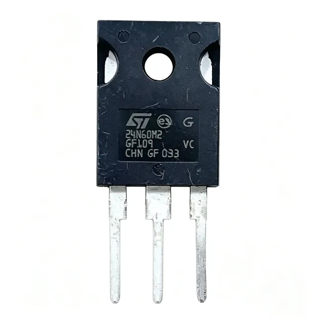
STW18N60M2 - 650V 18A N-Channel Power MOSFET | STMicroelectronics
The STW18N60M2 is an N-channel Power MOSFET manufactured by STMicroelectronics, featuring a breakdown voltage of 650V and a continuous drain current of 18A at 25°C. It is housed in a TO-247 package, which is a through-hole package suitable for high-power applications. This device is part of the MDmesh M2 series, which utilizes ST's advanced strip layout technology to achieve low on-resistance and reduced switching losses. A power MOSFET is a type of field-effect transistor designed to handle significant power levels in switching and amplification applications. It operates by controlling the flow of current through a semiconductor channel using an electric field, and it is widely used in power electronics for its high switching speed and efficiency. Power MOSFETs are a subset of discrete semiconductors, which are fundamental building blocks in power management and conversion systems. Key features of the STW18N60M2 include a low typical on-resistance of 0.19 ohm (at VGS=10V, ID=9A), a high avalanche ruggedness with an energy rating of 700 mJ, and a fast body diode with low reverse recovery charge. The device also offers a wide operating junction temperature range from -55°C to +150°C, making it suitable for demanding environments. The TO-247 package provides excellent thermal performance with a junction-to-case thermal resistance of 0.6°C/W, enabling efficient heat dissipation. The STW18N60M2 is built using ST's MDmesh M2 technology, which combines a vertical structure with a strip layout to minimize on-resistance and gate charge. This results in improved figure of merit (FOM) compared to previous generations, leading to higher efficiency in power conversion circuits. The device is designed for hard-switching topologies and offers a low gate charge of 45 nC, reducing driver requirements and switching losses. Typical applications include switch-mode power supplies (SMPS), power factor correction (PFC) circuits, and high-frequency DC-DC converters. In an SMPS, the STW18N60M2 can be used as the main switching element in the primary side, handling high voltage and current with minimal losses. Its low on-resistance ensures high efficiency, while its fast switching characteristics reduce electromagnetic interference (EMI). When designing with this device, ensure proper gate drive voltage (typically 10V) to achieve the lowest on-resistance. The device is not internally protected against overcurrent, so external current sensing and protection circuitry are recommended. Additionally, a proper snubber circuit may be required to manage voltage spikes during switching transitions.
STW20N60M2 - 600V 20A N-Channel Power MOSFET | STMicroelectronics
The STW20N60M2 is an N-channel Power MOSFET from STMicroelectronics' MDmesh M2 series, designed for high-efficiency power conversion applications. It features a breakdown voltage of 600V and a continuous drain current of 20A at 25°C, with a low on-resistance of 0.19 ohm typical. The device is housed in a TO-247 package, which provides excellent thermal performance for high-power applications. A Power MOSFET is a type of field-effect transistor optimized for switching and amplification of power. It operates by controlling the conductivity between the drain and source terminals through an insulated gate voltage. Power MOSFETs are essential components in power electronics, serving as switches in DC-DC converters, AC-DC power supplies, motor drives, and inverters. They are preferred for their fast switching speeds, high input impedance, and low drive power requirements compared to bipolar junction transistors. Key features of the STW20N60M2 include a low gate charge (Qg) of 45 nC, which reduces switching losses and enables high-frequency operation. The device also offers a fast body diode with low reverse recovery charge, making it suitable for bridge topologies. The MDmesh M2 technology provides an excellent figure of merit (RDS(on) x Qg), balancing conduction and switching losses for optimal efficiency. The STW20N60M2 utilizes a vertical DMOS structure with a striped layout, optimizing current distribution and thermal performance. The TO-247 package offers a low thermal resistance of 0.5°C/W (junction-to-case), allowing efficient heat dissipation. The device is avalanche-rated, with an avalanche energy of 1.2 J, ensuring robustness in inductive load switching. Typical applications include switch-mode power supplies (SMPS), power factor correction (PFC) circuits, solar inverters, and motor drives. The high voltage rating and low on-resistance make it ideal for 400V bus systems and 3-phase rectification. In PFC boost converters, the low gate charge enables high switching frequencies, reducing magnetic component size. When designing with this device, ensure proper gate drive voltage (typically 10V to 15V) to achieve low RDS(on). A gate resistor may be needed to control switching speed and reduce EMI. Adequate heatsinking is essential for continuous operation at high currents, as power dissipation can exceed 100W in worst-case conditions.
STW26N60M2 - 600V 26A N-Channel Power MOSFET | STMicroelectronics
The STW26N60M2 is an N-channel Power MOSFET manufactured by STMicroelectronics, designed for high-efficiency power conversion applications. It features a breakdown voltage of 600V and a continuous drain current of 26A at 25°C, making it suitable for a wide range of industrial and consumer power systems. The device is housed in a TO-247 package, which provides excellent thermal performance and is widely used in power electronics. A Power MOSFET is a type of field-effect transistor specifically designed to handle high voltages and currents in switching and amplification applications. It operates by controlling the flow of current through a semiconductor channel using an electric field, offering fast switching speeds and low on-resistance compared to bipolar transistors. Power MOSFETs are essential components in power management systems, where they function as switches in DC-DC converters, motor drives, and power supplies, enabling efficient energy conversion and regulation. Key features of the STW26N60M2 include a low on-resistance (RDS(on)) of typically 0.125 ohm at VGS=10V, which minimizes conduction losses and improves overall efficiency. The device also offers a fast switching performance with a total gate charge (Qg) of 78 nC, reducing switching losses in high-frequency applications. Additionally, it has a wide operating temperature range from -55°C to +150°C, ensuring reliability in harsh environments. The TO-247 package provides a low thermal resistance of 0.5°C/W (junction-to-case), enabling efficient heat dissipation. The STW26N60M2 utilizes STMicroelectronics' MDmesh M2 technology, which combines a vertical structure with a deep trench gate to achieve a good trade-off between on-resistance and switching performance. This technology enhances the device's robustness against avalanche breakdown and improves its body diode characteristics, making it suitable for bridge topologies and inductive load switching. The device also features a built-in gate-source ESD protection, enhancing its durability during handling and operation. Typical applications include switch-mode power supplies (SMPS), power factor correction (PFC) circuits, motor control, and uninterruptible power supplies (UPS). In these applications, the STW26N60M2 provides efficient switching and low conduction losses, contributing to higher system efficiency and reduced heat generation. Its high voltage rating and current capability make it ideal for 400V and 600V bus systems commonly found in industrial and telecom power supplies. When designing with this device, ensure proper gate driving to minimize switching losses and avoid parasitic turn-on. A gate resistor in the range of 10-100 ohm is recommended to control the switching speed and reduce EMI. Additionally, adequate heat sinking is required to maintain the junction temperature within safe limits, especially when operating at high currents and ambient temperatures.
STW30N60M2 - 600V 30A N-Channel Power MOSFET | STMicroelectronics
The STW30N60M2 is an N-channel Power MOSFET from STMicroelectronics' MDmesh M2 series, designed for high-efficiency power conversion applications. It features a breakdown voltage of 600V and a continuous drain current of 30A at 25°C, with a low on-resistance of 0.098 ohm (typical) and a fast body diode. The device is housed in a TO-247 package, which provides excellent thermal performance for high-power applications. A power MOSFET is a type of field-effect transistor designed to handle significant power levels in switching and amplification circuits. It operates by controlling the flow of current through a semiconductor channel using an electric field, offering high switching speeds and low conduction losses. Power MOSFETs are fundamental building blocks in power electronics, forming the basis of switch-mode power supplies, motor drives, and inverters. They are part of the broader category of discrete semiconductors, which also includes diodes, thyristors, and IGBTs. Key features of the STW30N60M2 include a low gate charge (Qg) of 60 nC (typical), which reduces switching losses and enables high-frequency operation. The device also offers a wide safe operating area (SOA) and is avalanche-rated, ensuring robustness in harsh environments. The TO-247 package has a thermal resistance of 0.5°C/W (junction-to-case), allowing efficient heat dissipation when mounted on a suitable heatsink. The STW30N60M2 utilizes STMicroelectronics' MDmesh M2 technology, which combines a vertical structure with a deep trench gate to achieve low on-resistance and reduced capacitance. This results in improved figure of merit (FOM) compared to previous generations, making it suitable for high-efficiency designs. The device also features a fast intrinsic body diode with low reverse recovery charge, which is critical for bridge topologies where diode recovery losses can dominate. Typical applications include switch-mode power supplies (SMPS), power factor correction (PFC) circuits, solar inverters, and motor drives. In an SMPS, the STW30N60M2 can be used as the main switching element in a flyback or forward converter, where its low RDS(on) minimizes conduction losses and its fast switching reduces transition losses. For PFC, the device's high voltage rating and low gate charge enable efficient boost converters operating at high frequencies. When designing with the STW30N60M2, ensure proper gate drive voltage (typically 10V to 15V) to fully enhance the channel and minimize on-resistance. The device is not internally protected against overcurrent, so an external current-sense resistor or fuse is recommended. Additionally, a gate resistor (e.g., 10 ohm) may be used to dampen ringing caused by parasitic inductance and capacitance.
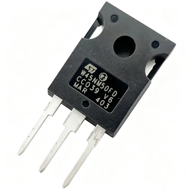
STW45NM50 - 45A, 500V N-Channel Power MOSFET | STMicroelectronics
The STW45NM50 is an N-channel Power MOSFET from STMicroelectronics, designed for high-efficiency power conversion applications. It features a drain-source voltage (VDS) of 500V, a continuous drain current (ID) of 45A at 25°C, and a low on-resistance (RDS(on)) of 0.09 ohm. The device is housed in a TO-247 package, which provides excellent thermal performance for high-power applications. A Power MOSFET is a type of field-effect transistor optimized for switching and amplification of power. It operates by controlling the flow of current through a semiconductor channel using an electric field, offering fast switching speeds and low conduction losses. Power MOSFETs are fundamental building blocks in power electronics, forming the basis of power management systems, motor drives, and switch-mode power supplies. They are part of the broader category of discrete semiconductors, which also includes diodes, thyristors, and IGBTs. Key features of the STW45NM50 include a low gate charge (Qg) of 120 nC, which enables fast switching and reduced driver requirements. The device also features a high avalanche ruggedness, with an avalanche energy rating of 1.2 J, making it suitable for applications where inductive loads are present. The TO-247 package offers a low thermal resistance of 0.5°C/W, allowing efficient heat dissipation in high-power designs. The STW45NM50 utilizes ST's proprietary MDmesh technology, which reduces on-resistance and gate charge compared to conventional MOSFETs. This technology enhances the device's efficiency and switching performance, making it ideal for high-frequency power conversion circuits. The device also includes an integrated body diode with fast recovery characteristics, reducing switching losses in bridge topologies. Typical applications include switch-mode power supplies (SMPS), power factor correction (PFC) circuits, motor drives, and uninterruptible power supplies (UPS). The high voltage rating and low on-resistance make it suitable for 400V and 500V bus systems commonly found in industrial and telecom equipment. When designing with this device, ensure proper gate drive voltage (typically 10V to 15V) to fully enhance the channel and minimize conduction losses. The device is RoHS compliant and halogen-free, meeting modern environmental standards. For automotive applications, consider the AEC-Q101 qualified variants if available.

STW45NM60 - 600V 45A MDmesh Power MOSFET | STMicroelectronics
The STMicroelectronics STW45NM60 is an N-channel 600 V, 45 A MDmesh Power MOSFET housed in a TO-247-3 through-hole package, designed using STMicroelectronics' proprietary MDmesh technology that combines a multiple-drain process with the company's PowerMESH horizontal layout. The device features a typical on-resistance of 90 mΩ at 10 V gate drive and 110 mΩ at 4.5 V, with a maximum continuous drain current of 45 A at Tc and a power dissipation rating of 417 W at Tc. A Power MOSFET is a voltage-controlled semiconductor switch used to efficiently switch and conduct current in power-conversion circuits. N-channel MOSFETs are the most common type due to their lower on-resistance per unit area compared to P-channel counterparts. The MDmesh family sits within STMicroelectronics' high-voltage MOSFET hierarchy (MDmesh -> PowerMESH -> Power MOSFET -> discrete semiconductor), targeting switched-mode power supply (SMPS) primary-side switches, motor-control inverters, and uninterruptible power supply (UPS) stages. Key features include a 600 V drain-source breakdown voltage rating, 90 mΩ typical Rds(on) at Vgs=10 V, and an outstanding dv/dt capability plus excellent avalanche ruggedness. The strip-based process yields overall dynamic performance that is significantly better than competing similar products. The TO-247 package provides high thermal-mass dissipation needed at 45 A continuous operation. Typical applications include high-power switched-mode power supply (SMPS) primary switches, three-phase inverter bridges for motor drives, induction heating, welding converters, photovoltaic string inverters, and uninterruptible power supply (UPS) front-end PFC and bridge stages. The 600 V rating provides ample headroom above 400 V PFC bus rails. When designing with this device, gate-drive voltage must reach 10 V for full enhancement to achieve the lowest Rds(on). At full 45 A load, ensure heatsink thermal resistance keeps Tj below 150 °C, and gate-source protection with a Zener clamp is recommended in motor-control environments where dv/dt stresses are severe. This page synthesizes distributor pricing, drop-in alternatives, and practical design notes not found in the manufacturer datasheet.
STW45NM60-H - 600V 45A MDmesh N-Channel Power MOSFET | STMicroelectronics
The STMicroelectronics STW45NM60-H is an N-channel 600 V, 45 A MDmesh power MOSFET housed in a TO-247-3 through-hole package with a typical on-resistance of 90 mΩ. Built on ST's revolutionary MDmesh technology that pairs a multiple-drain process with the proprietary PowerMESH horizontal layout, it achieves an outstandingly low RDS(on), high dv/dt capability, and excellent avalanche ruggedness for demanding high-voltage switching. Key specifications include a 600 V drain-source breakdown voltage (650 V at TJMAX), 45 A continuous drain current at 25 °C case, and 417 W total power dissipation. The device offers a typical on-resistance of 0.09 Ω at VGS = 10 V, gate threshold of 4 V, and 100% avalanche-tested ruggedness. The TO-247-3 through-hole package delivers superior thermal dissipation for high-current switching topologies. What is a MOSFET? A MOSFET (Metal-Oxide-Semiconductor Field-Effect Transistor) is a voltage-controlled semiconductor switch used for power conversion. Within the MOSFET family, power MOSFETs are classified into categories such as planar MOSFETs, trench MOSFETs, and super-junction (charge-balance) MOSFETs. The MDmesh family - where this STW45NM60-H belongs - is a super-junction N-channel MOSFET optimized for high-voltage (>500 V) switching applications. The STW45NM60-H is a discrete power transistor used in power management and conversion circuits. Architecture-wise, the MDmesh cell combines a multi-drain vertical structure with horizontal PowerMESH metallization, producing a higher power density than competing planar MOSFETs while lowering conduction losses. The strip-layout technique minimizes dynamic drain-source capacitance, reducing switching losses in hard-switched converters such as PFC stages and half-bridge converters. Typical applications include switched-mode power supplies (SMPS) with PFC, high-voltage DC-DC converters, industrial motor drives, uninterruptible power supplies (UPS), welding equipment, and induction-heating inverter stages operating from rectified 230 V or 400 V mains. When designing with this device, ensure adequate heat-sinking - the 417 W dissipation rating is only attainable with a substantial thermal interface. For high-frequency hard-switching topologies, gate-drive resistors in the 10-47 Ω range limit ringing, while a small RC snubber across the drain-source terminals mitigates voltage spikes caused by transformer leakage inductance. This page synthesizes distributor pricing, drop-in alternatives, and practical design notes that are not available in the manufacturer datasheet alone, giving design engineers a complete parametric view for sourcing decisions.

SUM60061EL-GE3 - 80V 150A P-Channel TrenchFET MOSFET | Vishay
The Vishay Siliconix SUM60061EL-GE3 is a P-Channel TrenchFET power MOSFET rated at 80 V VDS and 150 A continuous drain current (Tc) with 375 W power dissipation (Tc), housed in a surface-mount TO-263 (D2PAK) package. The '-GE3' suffix indicates the device is supplied lead-free and halogen-free, fully RoHS-compliant, with a matte-tin finish qualified for high-reflow soldering profiles. It is a member of the SUM6xxxx TrenchFET family, a line of P-channel MOSFETs designed for high-current switching applications where low on-resistance and high avalanche ruggedness are required. A P-channel MOSFET (PMOS) is a majority-carrier field-effect transistor whose channel is composed of p-type carriers (holes). PMOS devices simplify high-side switching circuits because they turn ON when the gate is pulled below the source, eliminating the need for a bootstrap or charge-pump circuit that N-channel high-side switches typically require. The SUM6xxxx family falls under the broader hierarchy of: P-channel MOSFET -> power MOSFET -> discrete semiconductor -> power management component. Key features of the SUM60061EL-GE3 include an extremely low typical on-resistance (RDS(on)) in the single-digit milliohm range at VGS = -10 V, fast switching, and 100% Rg and UIS (unclamped inductive switching) tested for avalanche ruggedness. The TO-263 (D2PAK) surface-mount package exposes a large metal tab for direct PCB heatsinking, enabling continuous high-current operation on FR-4 boards with proper copper-pour design. The SUM60061EL-GE3 uses Vishay's proprietary TrenchFET silicon technology, which etches vertical trenches into the silicon die to dramatically increase channel density per unit area. This produces lower RDS(on) per die size than planar MOSFETs, reducing conduction losses and improving thermal performance in compact surface-mount designs. Typical applications include power-OR-ing in redundant supply systems, battery protection and load switching in 48 V telecom rails, motor-drive reverse-battery protection, eMobility and forklift controllers, hot-swap circuits on server backplanes, and synchronous-rectifier secondary-side switching in industrial SMPS. Designers favor it when a logic-level P-channel high-side switch must drop minimal voltage at high current. When designing with this device, ensure VGS(th) is exceeded by a healthy margin at logic high levels, and provide adequate copper-pour area on the TO-263 tab to keep junction temperature below 175 C. Because P-channel MOSFETs carry current through the body diode during dead-time in half-bridge topologies, account for reverse-recovery loss if used as a synchronous rectifier. The lead-free (Sn) finish supports peak reflow temperatures up to 260 C per IPC/JEDEC J-STD-020. This page synthesizes distributor pricing, drop-in TrenchFET alternatives, and practical PCB thermal guidance not found in the manufacturer datasheet alone.

TJ30S06M3L(T6L1 - P-Ch 60V 30A 21.8mΩ DPAK+ MOSFET | Toshiba
The Toshiba TJ30S06M3L(T6L1 is a P-channel enhancement-mode power MOSFET built on Toshiba's U-MOS silicon process, rated for -60 V VDS, -30 A continuous drain current (Tc), and 68 W power dissipation, housed in a surface-mount DPAK+ (TO-252-3) package. According to the Toshiba datasheet, it delivers a typical RDS(ON) of 16.8 mΩ at VGS = -10 V and a maximum RDS(ON) of 21.8 mΩ, with a gate threshold of -3.0 V (VDS = -1 mA) and maximum leakage IDSS of -10 µA at VDS = -60 V. The (T6L1,NQ suffix denotes the tape-and-reel packaging variant aimed at high-volume automotive and industrial assembly lines. A P-channel MOSFET is a voltage-controlled transistor in which a negative gate-source voltage creates a conductive P-type channel between source and drain. Unlike N-channel MOSFETs, P-channel devices can be placed on the high-side of a load without a charge pump, simplifying reverse-polarity protection, load switching, and high-side drive circuits. P-channel MOSFETs sit within the broader power-MOSFET taxonomy: power MOSFET > MOSFET > field-effect transistor > discrete semiconductor, making them a foundational building block in modern switching power conversion. Key differentiating features of the TJ30S06M3L(T6L1 include AEC-Q101 automotive qualification, an ultra-low RDS(ON) of 16.8 mΩ typical that minimizes conduction losses, and a low gate charge suitable for high-frequency switching. The -3.0 V typical Vth allows direct CMOS/TTL logic-level driving without a gate driver in many applications. Built on Toshiba's U-MOS process, the cell pitch is optimized for the 60 V breakdown class to balance RDS(on), switching speed, and avalanche ruggedness. The DPAK+ package offers an exposed thermal pad and a tab that doubles as the drain terminal, achieving a junction-to-case thermal resistance (RθJC) suitable for 68 W continuous dissipation with adequate PCB copper. Typical applications include automotive motor drivers (power seats, window lifts, fuel pumps, fans), DC-DC converters (buck and buck-boost topologies), switching voltage regulators, reverse-battery protection circuits, and high-side load switches in industrial PLCs and battery management systems. The 60 V drain rating provides comfortable headroom for 12 V and 24 V automotive bus transients while supporting 48 V mild-hybrid loads in newer systems. When designing with this MOSFET, verify that VGS does not exceed the ±20 V absolute maximum rating, and place the gate-source pull-down resistor (typically 10 kΩ-100 kΩ) directly across the gate-source pins to prevent accidental turn-on from leakage or dv/dt-induced Miller coupling. Use a low-impedance gate-drive path with appropriate series resistance to limit ringing and overshoot in high-di/dt switching applications. This page synthesizes distributor stock data, drop-in alternatives from verified cross-references, and practical PCB layout notes not collected in the manufacturer datasheet, giving engineers a faster path to qualified sourcing and replacement decisions for the TJ30S06M3L(T6L1.
TJ50S06M3L - P-Ch 60V 50A 10.3mΩ U-MOSVI MOSFET | Toshiba
The Toshiba TJ50S06M3L is a P-channel enhancement-mode power MOSFET built on Toshiba's latest-generation U-MOSVI silicon process, rated for -60 V VDS, -50 A continuous drain current (Tc), and a typical RDS(on) of 10.3 mΩ at VGS = -10 V, housed in a surface-mount DPAK+ (TO-252-3) package. Its 90 W (TC) power dissipation and 13.8 mΩ maximum on-resistance position it as a high-current, low-loss switching element for automotive motor drivers, DC-DC converters, and switching voltage regulators. The device is qualified to AEC-Q101 for automotive-grade reliability, and the gate is rated for +10 V / -20 V VGS with a low threshold suitable for direct gate-drive from logic-level or standard MOSFET drivers. A P-channel MOSFET (P-ch) is a voltage-controlled field-effect transistor in which the channel region between source and drain is formed by inversion of n-type silicon under a negative gate-source voltage. Unlike N-channel MOSFETs (which require a gate drive above the source, often necessitating a charge pump or bootstrap), P-channel MOSFETs simplify high-side switching because their source sits at the load supply rail and a simple pull-down (or logic-low) gate signal turns them on. P-ch devices are commonly used in load switching, reverse-battery protection, motor reverse-braking, and high-side half-bridge or synchronous-rectifier positions where ease of drive outweighs the on-resistance penalty inherent to P-channel silicon. Key differentiating features of the TJ50S06M3L include Toshiba's U-MOSVI cell structure, which optimizes the trade-off between RDS(on) × Qg figure-of-merit and avalanche ruggedness. The 13.8 mΩ max RDS(on) at VGS = -10 V delivers low conduction loss in 30-40 A continuous-load paths, while the small TO-252-3 footprint allows direct substitution for legacy D-PAK footprints. The part also integrates a body-drain diode for synchronous-rectifier and freewheeling applications. Typical applications span automotive electronic power steering (EPS), brushless DC (BLDC) motor drivers for HVAC blowers and water pumps, 12 V bidirectional DC-DC converters in mild-hybrid systems, load switches and high-side OR-ing for redundant supplies, and switching voltage regulators. It is also a strong candidate for industrial-aggressive robotics, e-bike controllers, and battery management protection FET positions. When designing with this device, ensure the gate-source rating of +/-20 V is never exceeded and that adequate thermal copper (>=1 sq. inch of 2 oz pour) is provided under the DPAK+ tab. P-channel parts dissipate heat through the drain tab; do not rely on plastic-only thermal dissipation. This page synthesizes distributor pricing, drop-in alternatives, and practical design notes not found in the manufacturer datasheet.
TJ60S06M3L - P-Ch 60V 60A 11.2mΩ U-MOSVI MOSFET | Toshiba
The Toshiba TJ60S06M3L is a P-channel enhancement-mode power MOSFET built on the U-MOSVI silicon process, rated for -60 V VDS, -60 A continuous drain current, and a maximum power dissipation of 100 W (Tc). It is housed in a surface-mount DPAK+ (TO-252-3 lead-form) package with a typical on-resistance of 11.2 mΩ at VGS = -10 V, making it suitable for high-current switching applications. A Power MOSFET (Metal-Oxide-Semiconductor Field-Effect Transistor) is a voltage-controlled three-terminal semiconductor used for switching and amplifying signals in power electronics. P-channel MOSFETs specifically conduct when a negative gate-source voltage is applied, making them ideal for high-side switching where one terminal sits at the load supply. The TJ60S06M3L belongs to the U-MOSVI generation, which Toshiba's datasheet describes as offering low on-resistance, low leakage, and a -3.0 V enhancement-mode threshold for low-voltage gate drive compatibility. Key electrical characteristics include RDS(ON) of 11.2 mΩ (typ.) at VGS = -10 V, a low drain leakage IDSS of -10 µA (max) at VDS = -40 V, and an enhancement-mode threshold Vth of -3.0 V measured at VDS = -1 mA. The 7760 pF typical input capacitance (consistent with the Mouser datasheet snippet) reflects a die optimized for low gate charge rather than ultra-fast switching. The DPAK+ package provides a tab that acts as the drain connection and the primary thermal path, supporting sustained 60 A operation with proper heatsinking. Architecturally, this part uses Toshiba's U-MOSVI trench cell structure, which reduces cell pitch to lower on-resistance per unit area while keeping the Miller plateau modest. The result is a P-channel die that competes with similarly rated N-channel parts in 60 V class, but in a package commonly chosen for high-side load switching. The automotive-grade LJ suffix (AEC-Q101 qualified) is also available, designated TJ60S06M3L,LXHQ. Typical applications include high-side load switches in automotive ECUs, motor driver H-bridges, DC-DC converter high-side switches, and switching voltage regulators. Its low RDS(ON) reduces conduction loss in continuous-current paths such as reverse-battery protection circuits. Design considerations include keeping the gate-source loop area small to minimize ringing at turn-on, and ensuring the source-pin PCB copper area is sufficient to carry the full 60 A without excessive voltage drop.
TJ60S06M3L(T6L1,NQ - 60V 60A P-Ch MOSFET DPAK+ | Toshiba
The Toshiba TJ60S06M3L(T6L1,NQ is a P-channel silicon power MOSFET rated at -60 V VDS, -60 A continuous drain current, and 100 W power dissipation, housed in a surface-mount DPAK+ (TO-252-3) package. Built on Toshiba's U-MOS process, it delivers a typical on-resistance of 11.2 mOhm at VGS = -10 V and a typical threshold voltage of -3.0 V, achieving a figure of merit that suits high-current switching applications. The device is qualified to AEC-Q101 for automotive reliability. A P-channel MOSFET (P-FET) is a type of metal-oxide-semiconductor field-effect transistor in which the body-source p-n junction is reversed-biased and majority-carrier conduction is by holes rather than electrons. P-channel MOSFETs belong to the broader category of power MOSFETs (MOSFET -> discrete semiconductor -> power transistor), and they occupy a unique role in high-side switching because their source sits at the load supply rail, simplifying gate drive when the load must be switched to ground. P-FETs are commonly used as reverse-polarity protection devices, high-side load switches, and synchronous-rectifier replacements in low-voltage buck converters. Key features of the TJ60S06M3L include a maximum drain-source on-resistance RDS(ON) of 14.5 mOhm at VGS = -10 V, a low input capacitance Ciss of 7760 pF that keeps gate-drive losses manageable, and an enhancement-mode threshold that allows direct logic-level gate drive from -3.3 V or -5 V microcontrollers. The DPAK+ tab provides a low-thermal-resistance path (junction-to-case) suitable for continuous high-current operation with modest PCB copper area. The architecture uses Toshiba's latest-generation U-MOS trench cell, which lowers specific on-resistance versus older planar P-FET generations, and integrated gate-protection circuitry to limit avalanche energy. Compared with a mechanical relay, the MOSFET offers silent, fast (<50 ns half-controlled) switching and zero contact bounce, while compared with a PNP bipolar transistor it eliminates base-drive current and the saturation-voltage knee. Typical applications for this part include automotive reverse-battery protection, DC-DC converter high-side switches, motor-driver H-bridges (low-side or high-side position), and switching voltage regulators in industrial power systems. Because of its 60 V rating it can replace mechanical relays in 24 V and 48 V automotive and industrial buses. Design tip: when using the TJ60S06M3L as a reverse-polarity protection FET, ensure that the gate is pulled to ground through a resistor when the system is off; floating gates can leave the FET in an undefined state and create leakage paths. Also note that the AEC-Q101 grade makes this part suitable for under-hood automotive designs where ambient temperatures can reach 125 C.
TJ60S06M3L(T6L1,NQ - P-Ch -60V -60A 11.2mOhm DPAK+ MOSFET | Toshiba
The Toshiba TJ60S06M3L(T6L1,NQ is a P-channel silicon power MOSFET built on Toshiba's U-MOS process, rated for -60 V VDS, -60 A continuous drain current (TC), and a maximum power dissipation of 100 W. Housed in a surface-mount DPAK+ (TO-252 with extended leads) package, it delivers an ultra-low on-resistance of 0.0112 ohm at VGS = -10 V, with an input capacitance (Ciss) of 7760 pF. A P-channel MOSFET is a voltage-controlled field-effect transistor in which the conductive channel is formed by holes rather than electrons. Because P-channel devices turn on with a negative gate-source voltage, they simplify high-side switching in circuits where the load is tied to ground - no charge pump or bootstrap network is needed to drive the gate. P-channel MOSFETs are typically placed in the power-MOSFET hierarchy under 'P-channel -> MOSFET -> power MOSFET -> discrete semiconductor' and are widely used as reverse-polarity protection, high-side load switches, and synchronous-rectifier complements in DC-DC converters. Key features of the TJ60S06M3L include the very low 11.2 milliohm Rds(on) at full gate drive, the -60 V drain rating that provides substantial avalanche headroom for 12 V / 24 V automotive buses, and an industry-standard DPAK+ footprint that allows direct PCB mounting with a thermal pad for low thermal resistance. The part is qualified for automotive motor drivers, DC-DC converters, and switching voltage regulators per Toshiba's product family positioning. Technically, the device uses Toshiba's latest-generation U-MOS trench cell structure to achieve a per-cell figure-of-merit (FOM = Rds(on) x Qg) optimized for switching loss reduction. This makes it particularly suitable for hard-switched applications up to several hundred kHz where switching losses dominate conduction losses. The P-channel polarity allows direct logic-level driving from standard microcontrollers without additional gate-driver circuitry. Typical applications include automotive ECU load switching, motor-driver H-bridge high-side switches, battery management system (BMS) reverse-polarity protection, synchronous-rectifier secondary-side switches in isolated DC-DC converters, and high-current load management in industrial 24 V systems. The DPAK+ package's exposed thermal pad allows direct PCB heatsinking. When designing with this device, mind the gate-source voltage rating of +10 V / -20 V - the absolute maximum must not be exceeded even during transients. Use a gate-source resistor (typically 10 kohm) to prevent inadvertent turn-on from Miller-coupling during drain-voltage transients. Verify continuous drain current against your thermal envelope using the SOA curve from the manufacturer datasheet. This page synthesizes distributor pricing, drop-in alternatives, and practical design notes not found in the manufacturer datasheet alone, providing a single reference for sourcing and second-sourcing the TJ60S06M3L(T6L1,NQ.
VND7NV04TR-E - 45V 6A OMNIFET II Auto-Protected MOSFET | STMicroelectronics
The STMicroelectronics VND7NV04TR-E is an OMNIFET II fully auto-protected N-channel power MOSFET rated for 45V drain-to-source voltage and 6A continuous drain current, housed in a 3-pin DPAK (TO-252) surface-mount package. It delivers a typical Rds(on) of 60 mOhm, integrates built-in thermal shutdown, linear current limitation, and an over-voltage clamp, and is intended as a solid-state replacement for standard Power MOSFETs in DC to 50 kHz switching applications. A high-side switch (also known as a smart power switch or fully-protected MOSFET) is a discrete power semiconductor that integrates the power MOSFET die with on-chip protection, diagnostic, and gate-drive circuitry into a single package. The OMNIFET II family belongs to ST's VIPower M0-3 technology platform, which combines vertical DMOS power structures with bipolar/mixed-signal control blocks. Compared to a discrete N-channel MOSFET that requires external protection, an OMNIFET II part reduces BOM count, PCB area, and design complexity while improving reliability in harsh electrical environments. Key parametric features include 45V Vdss maximum rating, 6A continuous output current, 60 mOhm typical Rds(on) at 25C, an input pin that draws minimal drive current, and a diagnostic feedback path that reports fault status by sensing voltage at the input pin. Built-in protections cover short-circuit current limiting, over-temperature shutdown, and over-voltage avalanche clamping. The DPAK package offers a low thermal resistance of approximately 50 C/W junction-to-ambient on a standard JEDEC 1 sq-in copper pad. Architecturally, the VND7NV04TR-E uses ST's VIPower M0-3 vertical DMOS cell array with monolithic bipolar analog control for protection and diagnostics. The fault feedback pin allows a microcontroller to detect open-load, short-to-ground, and over-temperature conditions without additional external sense circuitry. Operating switching capability extends from DC up to 50 kHz, covering most relay-replacement and load-driving tasks. Typical applications include automotive body modules (lamp drivers, solenoid and relay replacement), industrial PLC output stages, 12V/24V DC load switching, and any solid-state relay (SSR) function where a logic-level input must switch a high-current inductive or resistive load with integrated fault diagnostics. When designing with the VND7NV04TR-E, ensure the input pin receives proper logic-level drive, place the device on a copper pad sized for worst-case power dissipation (P = I^2 * Rds(on)), and add a TVS diode or freewheeling path if driving motors where back-EMF exceeds the avalanche rating. This page synthesizes distributor pricing, drop-in OMNIFET II alternatives, and practical design notes not found in the manufacturer datasheet alone.
ZXMHC6A07N8TC - 60V Complementary H-Bridge MOSFET | Diodes Inc
The Diodes Incorporated ZXMHC6A07N8TC is a 60V complementary enhancement-mode MOSFET H-bridge array integrating two N-channel and two P-channel MOSFETs in a single SO-8 (8-SO) surface-mount package. The N-channel pair is rated to 60V V(BR)DSS with 1.8A continuous drain current (1.39A per device in the dual configuration) and 0.25 ohm RDS(on) at VGS=10V, while the P-channel pair is rated to -60V with 1.4A continuous drain current (1.28A per device) and 0.40 ohm RDS(on) at VGS=-10V. Total package power dissipation is 870mW. A MOSFET H-bridge is a four-switch topology used to drive bidirectional current through a load (typically a DC motor, solenoid, or piezo element) by selectively activating diagonal pairs of N and P-channel devices. The complementary N+P architecture inside one package eliminates the need for external charge-pump or level-shift circuitry, simplifying PCB layout and reducing BOM count compared with discrete all-N-channel H-bridges that require a high-side bootstrap driver. H-bridge arrays sit at the lowest tier of the power semiconductor family, which itself belongs to the broader discrete semiconductor category. Key features include low on-resistance achievable with low gate-drive voltage (logic-level compatible at VGS=10V), monolithic die construction that minimizes parasitic inductance between the half-bridges, and a thermally enhanced SO-8 footprint with exposed center pad. The asymmetric N/P ratings (slightly higher RDS(on) on the P-channel) reflect typical silicon area trade-offs in complementary processes, and are well matched for the symmetric switching patterns of H-bridge operation. The device is also characterized for fast switching transitions, which reduces dead-time losses in PWM motor control. The architecture uses Diodes Incorporated's latest-generation TrenchMOS process, which achieves the low figure-of-merit (RDS(on) x Qg) needed for sub-1 ohm complementary switches in a small outline package. Internal source connections are bonded out individually on the package pins, allowing the four MOSFETs to be used either as a complete H-bridge or as two independent half-bridges for buck/boost converter legs. This dual-use flexibility is a notable advantage over H-bridges predriver/only ICs that lock the user into a fixed topology. Typical applications include DC motor driver H-bridges in low-voltage appliances, DC-AC inverters for LED backlighting and piezo buzzers, solenoid and valve drivers in industrial controls, and battery-powered robotic actuators. The 60V rating comfortably covers 12V and 24V industrial bus rails with substantial transient headroom. When designing with this device, ensure the gate-drive timing accounts for the slower P-channel turn-off (typical of PMOS in H-bridges) and provide adequate dead-time in PWM firmware to prevent cross-conduction. Place a low-ESR ceramic bypass capacitor directly at the package to suppress the VDS ringing that arises from the package lead inductance. This page synthesizes distributor pricing, drop-in alternatives, parametric comparison, and practical H-bridge design notes not found in the manufacturer datasheet alone.

ZXMP6A17GQ - 60V P-Ch MOSFET, 3A, SOT-223 | Diodes Inc
The Diodes Incorporated ZXMP6A17GQ is a 60V P-Channel Enhancement Mode MOSFET rated for 3A continuous drain current and 2W power dissipation in a SOT-223-3 (TO-261-4) surface-mount package. It combines a 125 mΩ typical on-resistance at VGS = -10V with a -4.3A pulsed current rating, and 190 mΩ typical RDS(on) at VGS = -4.5V delivering -3.5A, enabling low-loss high-side switching without bulky gate drivers. What is a P-Channel Enhancement Mode MOSFET? It is a specific type of metal-oxide-semiconductor field-effect transistor in which the conducting channel is formed by applying a negative gate-to-source voltage below the device threshold, allowing conventional positive-rail high-side switching when paired with N-Channel parts. As an enhancement-mode device it is normally off at VGS = 0V, sits within the MOSFET -> FET -> discrete semiconductor -> power management IC taxonomy, and is typically chosen for reverse-battery protection, load switching, and synchronous-rectifier low-side positions where ground-referenced control is preferred. Key features include fast switching speed for high-frequency PWM operation, low gate drive allowing direct logic-level control from 3.3V or 5V microcontrollers, low input capacitance (Ciss) minimising drive losses, and a Green / RoHS-compliant lead-free finish. The device is halogen- and antimony-free, qualifying it for modern environmental standards and high-reliability build requirements. Internally the part uses Diodes' proprietary TrenchFET generation, which shrinks the on-resistance per unit silicon area by orienting the conduction cells vertically through the epitaxial layer. The result is a 4-pin SOT-223 footprint with the tab as an additional thermal pad (pin 4), giving much lower RθJA than a 3-pin SOT-223 part while keeping the same PCB land pattern. Typical applications include automotive load switching and reverse-battery protection, DC-DC converter synchronous-rectifier low-side switches, battery management charge/discharge paths in power tools, motor-drive H-bridges, and hot-swap / in-rush current limiters in industrial 24V buses. The -Q suffix confirms IATF 16949 build, AEC-Q101 qualification, and PPAP capability. When designing with the ZXMP6A17GQ, place the tab-to-PCB copper pour area at least 100 mm² to keep RθJA below its rated value at 2W. Source the gate resistor at 10Ω-100Ω to dampen the high dv/dt produced by the low Ciss and use a pull-down of 10kΩ-100kΩ to keep the device off during controller reset. This page aggregates verified distributor pricing, AEC-Q101-aware drop-in alternatives, and application-grade design notes beyond the manufacturer datasheet summary to accelerate your selection.